

SGS Thomson Microelectronics TDA7439D, TDA7439B, TDA7439 Datasheet
DIGITALLY CONTROLLED AUDIO PROCESSOR
INPUTMULTIPLEXER
- 4 STEREO INPUTS
- SELECTABLEINPUT GAIN FOR OPTIMAL
ADAPTATIONTO DIFFERENT SOURCES
ONE STEREO OUTPUT
TREBLE, MIDDLE AND BASS CONTROL IN
2.0dB STEPS
VOLUMECONTROL IN 1.0dB STEPS
TWOSPEAKERATTENUATORS:
- TWOINDEPENDENTSPEAKERCONTROL
IN 1.0dBSTEPSFOR BALANCE FACILITY
- INDEPENDENTMUTE FUNCTION
ALL FUNCTION ARE PROGRAMMABLE VIA
SERIALBUS
TDA7439
THREE BANDS
SDIP30 DIP28
SO28
ORDERING NUMBERS: TDA7439 (SDIP30)
TDA7439B (DIP28)
TDA7439D (SO28)
DESCRIPTION
The TDA7439 is a volume tone (bass, middle and
treble) balance (Left/Right) processor for quality
audio applicationsin car-radio and Hi-Fi systems.
Selectable input gain is provided. Control of all
the functions is accomplishedby serialbus.
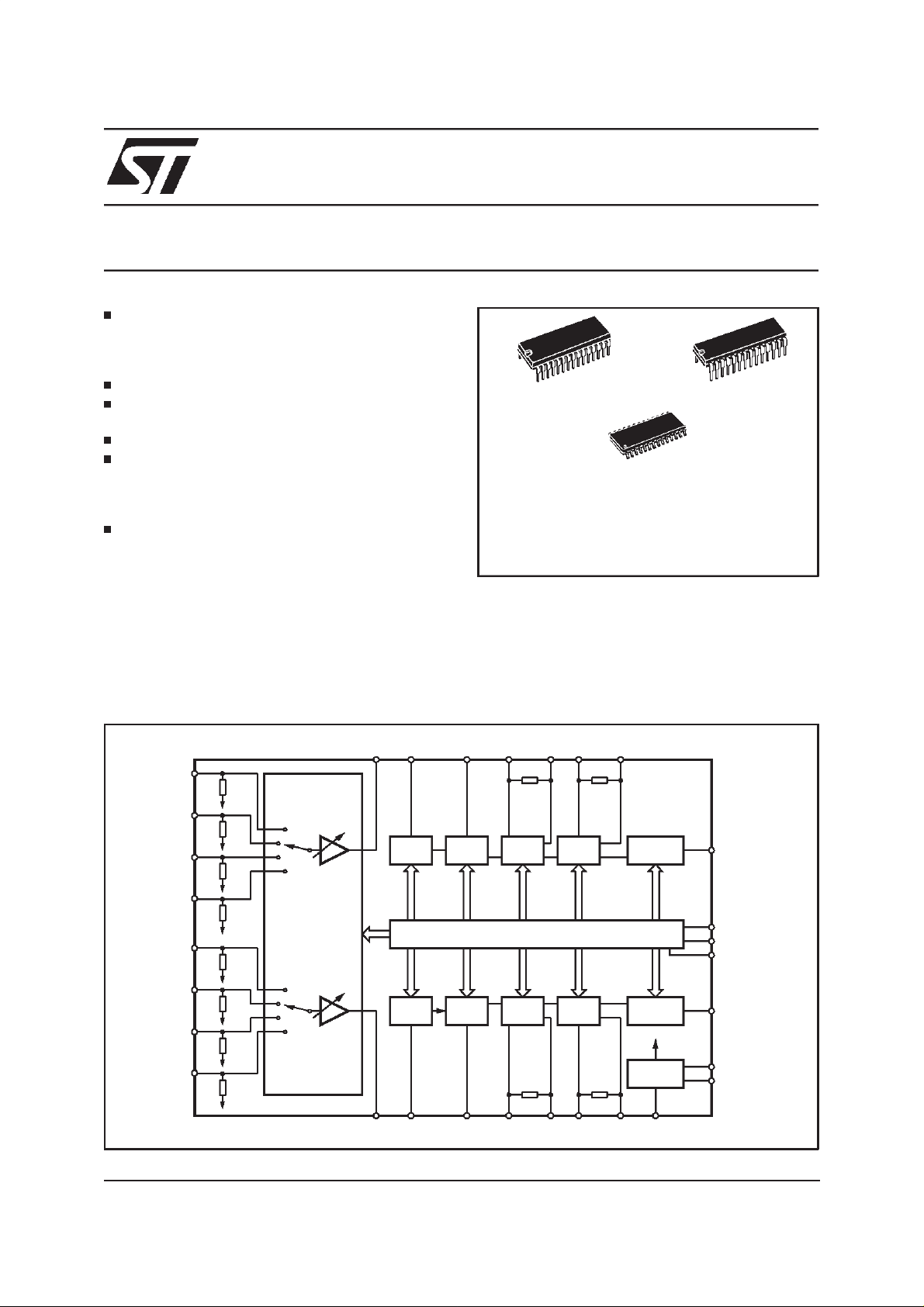
BLOCK DIAGRAM
L-IN1
L-IN2
L-IN3
L-IN4
R-IN1
R-IN2
R-IN3
R-IN4
11
12
13
14
10
9
8
7
(TDA7439)
100K
100K
100K
100K
100K
100K
100K
INPUT
100K
G
0/30dB
2dB STEP
G
MULTIPLEXER
+ GAIN
MUXOUTL INL
15 16 27 26 25 23 24
VOLUME
VOLUME
17 18 28 19 20 21 22 2
MUXOUTR INR TREBLE(R)
The AC signal setting is obtained by resistor networks and switches combined with operational
amplifiers.
Thanks to the used BIPOLAR/CMOSTechnology,
Low Distortion, Low Noise and DC stepping are
obtained
TREBLE(L)
MIN(L)
TREBLE
TREBLE
MIDDLE
I2CBUS DECODER + LATCHES
MIDDLE
MIN(R) MOUT(R) BOUT(R)BIN(R)
MOUT(L)
R
M
R
M
BIN(L)
BASS
BASS
R
B
R
B
BOUT(L)
SPKR ATT
LEFT
SPKR ATT
RIGHT
V
REF
SUPPLY
CREF
6
30
1
29
5
3
4
D95AU342B
LOUT
SCL
SDA
DIG_GND
ROUT
V
S
AGND
April 1999
1/19
TDA7439
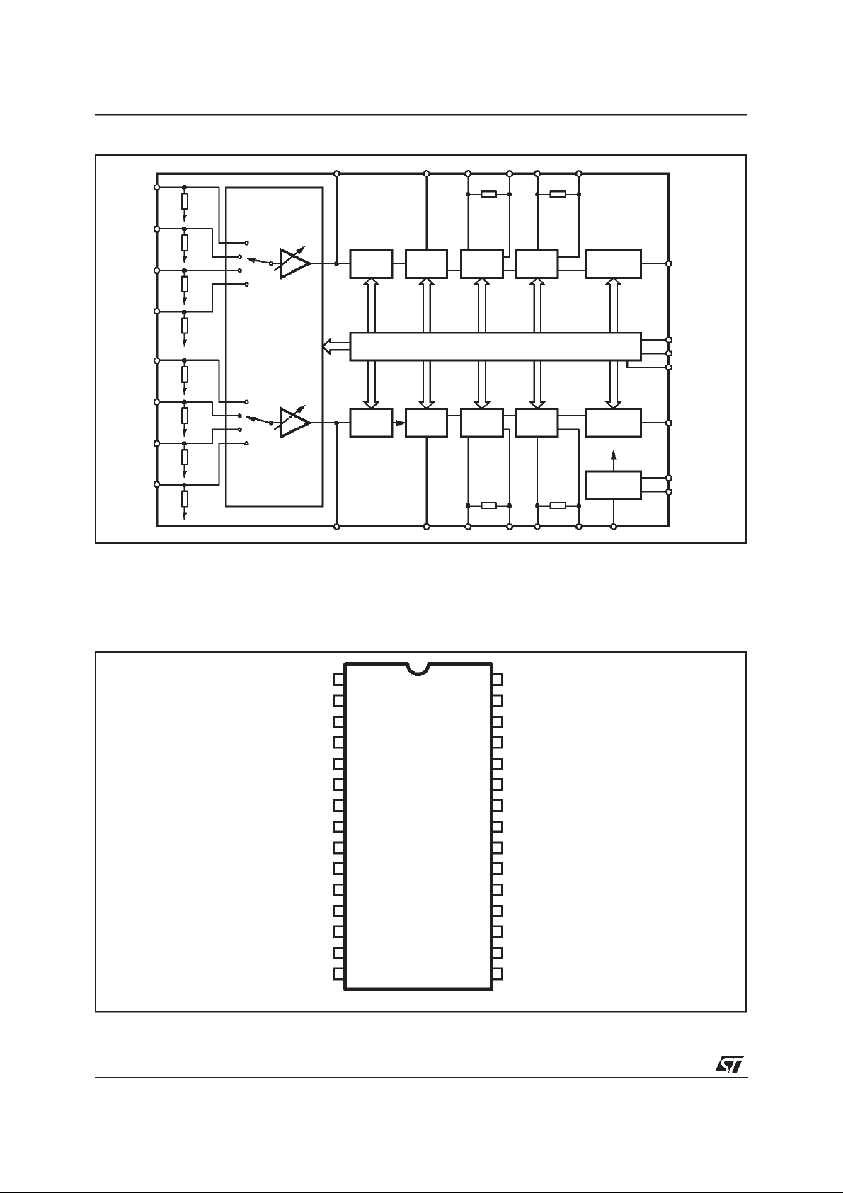
BLOCK DIAGRAM (TDA7439B/TDA7439D)
MUXOUTL
L-IN1
L-IN2
L-IN3
L-IN4
R-IN1
R-IN2
R-IN3
R-IN4
4
100K
5
100K
6
100K
7
100K
3
100K
2
100K
1
100K
28
100K
INPUT
G
0/30dB
2dB STEP
G
MULTIPLEXER
+ GAIN
8 1817161415
VOLUME
VOLUME
9 191011121323
MUXOUTR TREBLE(R)
TREBLE(L)
TREBLE
TREBLE
MIN(L)
MIDDLE
I2CBUS DECODER + LATCHES
MIDDLE
MIN(R) MOUT(R) BOUT(R)BIN(R)
MOUT(L)
R
M
R
M
BIN(L)
BASS
BASS
BOUT(L)
R
B
R
B
SPKR
LEFT
SPKR
RIGHT
V
REF
SUPPLY
CREF
ATT
ATT
27
21
22
20
26
24
25
LOUT
SCL
SDA
DIG_GND
ROUT
V
S
AGND
D97AU621
PIN CONNECTION (SDIP30)
MUXOUTL INL1615
1
2
V
AGND
ROUT MIN(L)
LOUT
R-IN4
R-IN3
R-IN2
R-IN1
L-IN1
L-IN2
L-IN3
L-IN4
3
S
4
5
6
7
8
9
10
11
12
13
14
D95AU340A
30
29
28
27
26
24
23
22
21
20
19
18
17
SCLSDA
DIG_GNDCREF
TREBLE(R)
TREBLE(L)
MOUT(L)25
BOUT(L)
BIN(L)
BOUT(R)
BIN(R)
MOUT(R)
MIN(R)
INR
MUXOUTR
2/19

PIN CONNECTION (DIP28/SO28)
TDA7439
R_IN3
R_IN2
R_IN1
L_IN1
L_IN2 V
L_IN3
L_IN4
MUXOUTL
MUXOUTR
MIN(R)
MOUT(R)
BIN(R)
BOUT(R)
BIN(L)
1
2
3
4
5
6
7
8
9
10
11
12
13
14
D97AU622
28
27
26
25
24
22
21
20
19
18
17
16
15
R_IN4
LOUT
ROUT
AGND
S
CREF23
SDA
SCL
DIG-GND
TREBLE(R)
TREBLE(L)
MIN(L)
MOUT(L)
BOUT(L)
ABSOLUTE MAXIMUM RATINGS
Symbol Parameter Value Unit
V
S
T
amb
T
stg
Operating Supply Voltage 10.5 V
Operating Ambient Temperature -10 to 85
Storage Temperature Range -55 to 150 °C
C
°
THERMAL DATA
Symbol Parameter Value Unit
R
thj-pin
Thermal ResistanceJunction-pins 85
QUICK REFERENCE DATA
Symbol Parameter Min. Typ. Max. Unit
V
V
CL
THD Total Harmonic Distortion V = 1Vrms f = 1KHz 0.01 0.1 %
S/N Signal to Noise Ratio V
S
Supply Voltage 6 9 10.2 V
S
Max. input signal handling 2 Vrms
= 1Vrms (mode = OFF) 106 dB
out
Channel Separation f = 1KHz 90 dB
C
Input Gain in (2dBstep) 0 30 dB
Volume Control (1dB step) -47 0 dB
Treble Control (2dB step) -14 +14 dB
Middle Control (2dB step) -14 +14 dB
Bass Control (2dB step) -14 +14 dB
Balance Control 1dB step -79 0 dB
Mute Attenuation 100 dB
C/W
°
3/19

TDA7439
ELECTRICALCHARACTERISTICS (refer tothe test circuit T
= 600Ω, all controlsflat (G = 0dB), unless otherwisespecified)
R
G
=25°C,VS= 9V,RL= 10KΩ,
amb
Symbol Parameter Test Condition Min. Typ. Max. Unit
SUPPLY
V
S
I
S
SVR Ripple Rejection 60 90 dB
Supply Voltage 6 9 10.2 V
Supply Current 4 7 10 mA
INPUT STAGE
G
G
R
V
S
G
IN
CL
IN
inmin
inman
step
Input Resistance 70 100 130 KΩ
Clipping Level THD = 0.3% 2 2.5 Vrms
Input Separation The selected input is grounded
80 100 dB
through a 2.2µ capacitor
Minimum Input Gain -1 0 1 dB
Maximum Input Gain 29 30 31 dB
Step Resolution 1.5 2 2.5 dB
VOLUMECONTROL
C
RANGE
A
A
V
A
R
VMAX
STEP
E
A
E
T
DC
mute
Input Resistance 20 33 50 K
i
Control Range 45 47 49 dB
Max. Attenuation 45 47 49 dB
Step Resolution 0.5 1 1.5 dB
Attenuation Set Error AV= 0 to-24dB -1.0 0 1.0 dB
A
= -24 to -47dB -1.5 0 1.5 dB
V
Tracking Error AV= 0 to-24dB 0 1 dB
= -24 to -47dB 0 2 dB
A
V
DC Step adjacent attenuation steps
from 0dB to A
V
max
0
0.5
Mute Attenuation 80 100 dB
3mV
BASS CONTROL(1)
Gb Control Range Max. Boost/cut +12.0 +14.0 +16.0 dB
B
STEP
R
B
Step Resolution 1 2 3 dB
Internal Feedback Resistance 33 44 55 KΩ
TREBLECONTROL(1)
Gt Control Range Max. Boost/cut +13.0 +14.0 +15.0 dB
T
STEP
Step Resolution 1 2 3 dB
MIDDLE CONTROL(1)
Gm Control Range Max. Boost/cut +12.0 +14.0 +16.0 dB
M
STEP
R
M
Step Resolution 1 2 3 dB
Internal Feedback Resistance 18.75 25 31.25 K
SPEAKERATTENUATORS
C
RANGE
S
STEP
E
A
V
DC
A
mute
NOTE1:
1) The device is functionally goodat Vs = 5V. a step down,on Vs, to 4V does’t reset thedevice.
2) BASS,MIDDLE and TREBLEresponse: The center frequency and theresponse quality can be chosen by the external circuitry.
Control Range 70 76 82 dB
Step Resolution 0.5 1 1.5 dB
Attenuation Set Error AV= 0 to-20dB -1.5 0 1.5 dB
A
= -20 to -56dB -2 0 2 dB
V
DC Step adjacent attenuation steps 0 3 mV
Mute Attenuation 80 100 dB
Ω
mV
Ω
4/19

TDA7439
ELECTRICALCHARACTERISTICS (continued.)
Symbol Parameter Test Condition Min. Typ. Max. Unit
AUDIOOUTPUTS
V
CLIP
R
L
R
O
V
DC
GENERAL
E
NO
E
t
S/N Signal to Noise Ratio All gains 0dB; V
S
C
d Distortion A
BUS INPUT
V
IL
V
IH
I
IN Input Current VIN = 0.4V -5 0 5 µA
V
O
Clipping Level d = 0.3% 2.1 2.6 V
Output Load Resistance 2 KΩ
Output Impedance 10 40 70
DC Voltage Level 3.5 3.8 4.1 V
Output Noise All gains = 0dB;
515
BW = 20Hz to 20KHz flat
Total Tracking Error AV= 0to -24dB 0 1 dB
= -24to -47dB 0 2 dB
A
V
O
=1V
; 95 106 dB
RMS
Channel Separation Left/Right 80 100 dB
V =0;VI=1VRMS ; 0.01 0.08 %
Input Low Voltage 1V
Input High Voltage 3 V
Output Voltage SDA
IO= 1.6mA 0.4 0.8 V
Acknowledge
RMS
Ω
V
µ
TEST CIRCUIT
L-IN1
0.47µF
L-IN2
0.47µF
L-IN3
0.47µF
L-IN4
0.47µF
R-IN1
0.47µF
R-IN2
0.47µF
R-IN3
0.47µF
R-IN4
0.47µF
5.6nF
2.2µF
11
100K
12
100K
13
100K
14
100K
10
100K
9
100K
8
100K
7
100K
INPUT MULTIPLEXER
MUXOUTL INL
G
0/30dB
2dB STEP
G
+ GAIN
MUXOUTR INR TREBLE(R)
TREBLE(L)
15 16 27 26 25 23 24
VOLUME
VOLUME
17 18 28 19 20 21 22 2
2.2µF
5.6nF
2.7K 5.6K
18nF 22nF 100nF 100nF
MIN(L)
MOUT(L)
R
M
TREBLE
TREBLE
MIDDLE
I2CBUS DECODER + LATCHES
MIDDLE
R
M
MOUT(R) BOUT(R)BIN(R)
MIN(R)
18nF 22nF 100nF 100nF
2.7K 5.6K
BIN(L)
BASS
BASS
BOUT(L)
R
B
SPKR ATT
LEFT
SPKR ATT
RIGHT
V
REF
R
SUPPLY
B
CREF
10µF
30
29
6
1
5
3
4
LOUT
SCL
SDA
DIGGND
ROUT
V
S
AGND
D95AU339B
5/19
TDA7439
APPLICATIONSUGGESTIONS
The first and the last stages are volume control
blocks. The control range is 0 to -47dB (mute) for
the first one, 0 to -79dB (mute) for the last one.
Both of them have 1dB step resolution.
The very high resolutionallows the implementation
of systemsfreefromanynoisyacousticaleffect.
The TDA7439 audioprocessor provides 3 bands
tones control.
Bass, Middle Stages
The Bass and the middle cells have the same
structure.
The Bass cell has an internal resistor Ri = 44KΩ
typical.
The Middle cell has an internalresistor Ri = 25KΩ
typical.
Several filter types can be implemented, connecting external components to the Bass/Middle IN
and OUTpins.
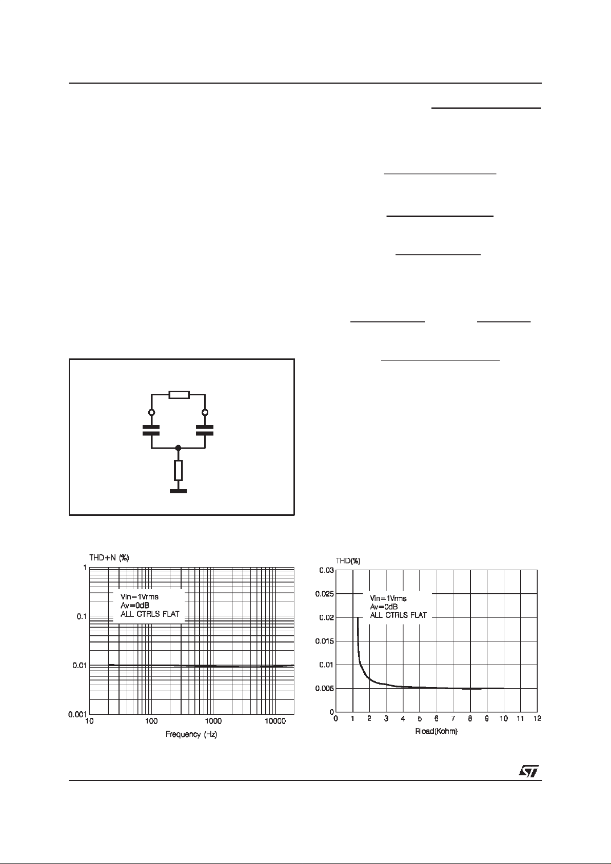
Figure 1.
Ri internal
OUTIN
C
1
R
2
D95AU313
C
2
The fig.1 refers to basic T Type Bandpass Filter
starting from the filter component values (R1 internal and R2,C1,C2 external) the centre frequency Fc, the gain Av at max. boost and the filter Q factorare computedas follows:
=
F
C
1
2 ⋅ π ⋅√R1 ⋅ R2 ⋅ C1 ⋅ C2
R2 C2 + R2 C1 + RiC1
A
=
V
R2 C1 + R2 C2
√R1 ⋅ R2 ⋅ C1 ⋅ C2
Q =
R2 C1 + R2 C2
Viceversa, once Fc, Av, and Ri internal value are
fixed, the external componentsvalues will be:
C1 =
− 1
A
V
2 ⋅ π ⋅ F
R2 =
⋅ Ri⋅ Q
C
A
− 1 − Q
V
2 ⋅ π ⋅ C1 ⋅ FC⋅ (AV− 1) ⋅Q
C2 =
2
Q
A
V
2
⋅ C1
− 1 − Q
2
TrebleStage
The treble stage is a high pass filter whose time
constant is fixed by an internal resistor (25KΩ
typical) and an external capacitor connected between treble pins andground
Typical responsesare reported in Figg. 10 to 13.
CREF
The suggested 10µF reference capacitor (CREF)
value can be reduced to 4.7µF if the application
requiresfasterpower ON.
Figure 2:
6/19
THD vs. frequency
Figure3:
THDvs. R
LOAD
 Loading...