


BASIC FUNCTION AUDIO PROCESSOR
ONE STEREOANDONE MONOINPUTS
MUTE FUNCTION (SOFTWARE AND HARD-
WARE) CONTROLLED
VOLUMECONTROL IN 1dB STEP
BASS ANDTREBLECONTROL IN 2dBSTEP
FULLY PROGRAMMABLE LOUDNESS CON-
TROL
FOURSPEAKERATTENUATORS:
– Independentattenuationcontrol
– Independentmutefunction
ALL FUNCTIONS PROGRAMMABLE VIA
2
CBUS
I
DESCRIPTION
The TDA7432 is a volume, tone (bass and treble)
balance (Left/Right) processor for quality audio
applicationsincar radio and Hi-Fi systems.
Control is accomplished by serial bus microprocessor interface.
The AC signal setting is obtained by resistor net-
TDA7432
SO20
ORDERING NUMBER: TDA7432D
works and switches combined with operational
amplifiers.
Thanks to the advanced BIPOLAR/CMOS Technology, the external components have been reduced.
BLOCK DIAGRAM
IN_L
MONO_IN/MUTE
IN_R
S
68nF
3
MUX
4
2
17
MUX
SUPPLYV
20
GND
10µF 2.7nF
68nF
VOL
+ LOUD
VOL
+ LOUD
4.7K
100nF100nF
BASS TREBLE
S BUS DECODER + LATCHES
BASS TREBLE
100nF100nF
4.7K
2.7nF
TRLBOUTLBINLLOUD_L
119106
127851
TRRBOUTRLOUD_R BINRCREF
SPKR
ATT
SPKR
ATT
SPKR
ATT
SPKR
ATT
16
14
18
19
15
13
D95AU357A
LEFT FRONT
LEFT REAR
SCL
SDA
RIGHT FRONT
RIGHT REAR
August 1996
1/10

TDA7432
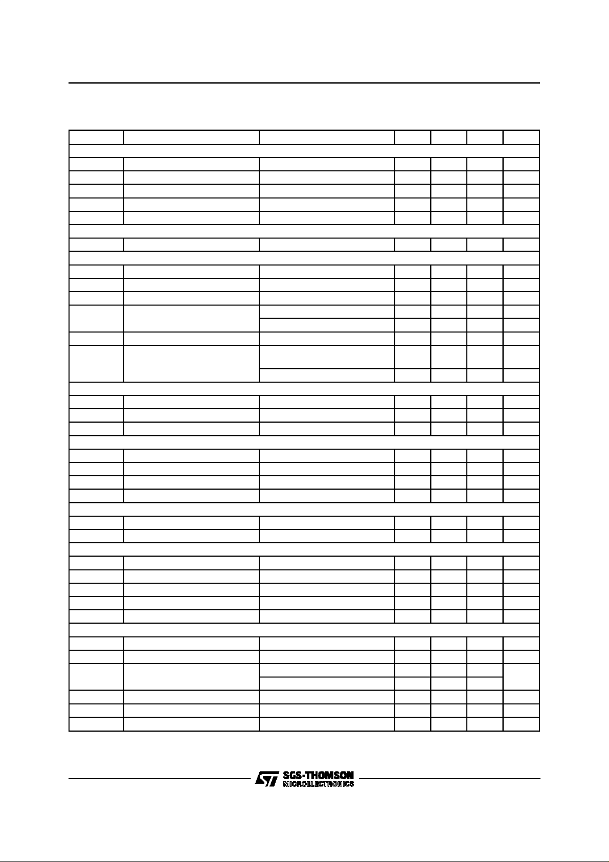
ABSOLUTE MAXIMUM RATINGS
Symbol Parameter Value Unit
V
S
T
amb
T
stg
QUICK REFERENCEDATA
Symbol Parameter Min. Typ. Max. Unit
V
S
V
CL
THD Total Harmonic Distortion (V = 1Vrms f = 1kHZ) 0.05 %
S/N Signal to Noise Ratio 102 dB
Sc Channel Separation f = 1kHz 100 dB
Operating Supply Voltage 10.2 V
Operating Temperature Range -40 to 85 °C
Storage Temperature Range -55 to +150 °C
Supply Voltage 7 9 10.2 V
Max. Input Signal Handling 1.3 1.6 Vrms
Volume Control 1dB step -79 +32 dB
Bass Control 2dB step -18 +18 dB
Treble Control2dB step -14 +14 dB
Speaker Attenuators -37.5 0 dB
Mute Attenuation 100 dB
PIN CONNECTION(Top View)
MONO_IN/MUTE
LOUD_R
LOUD_L
BOUT_R
BOUT_L TRR
CREF
IN_R
IN_L
2
3
4
5
6
7
BIN_R
8
9
BIN_L TRL
10
D95AU358
20
19
18
17
16
15
14
13
12
11
GND1
SDA
SCL
V
S
OUT_LF
OUT_RF
OUT_LR
OUT_RR
THERMAL DATA
Symbol Parameter Value Unit
Thermal ResistanceJunction-pins Max. 150 °C/W
2/10
R
th j-pins

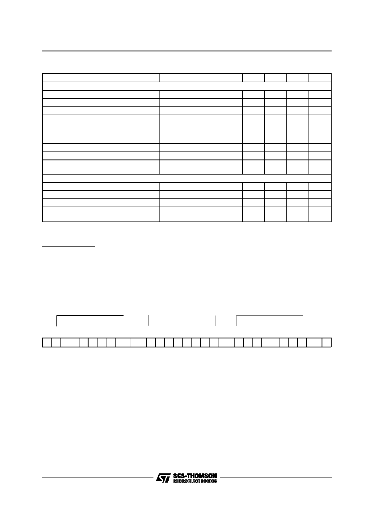
APPLICATIONCIRCUIT
TDA7432
68nF
IN_L
3
MUX
4
MONO_IN
/MUTE
IN_R
2
V
17
9V
V
S
100nF
S
MUX
SUPPLY
20
GND
4.7µF 2.7nF
68nF
VOL
+ LOUD
VOL
+ LOUD
4.7K
100nF100nF
BASS TREBLE
S BUS DECODER + LATCHES
BASS TREBLE
100nF100nF
4.7K
2.7nF
TRLBOUTLBINLLOUD_L
119106
127851
TRRBOUTRLOUD_R BINRCREF
SPKR
ATT
SPKR
ATT
SPKR
ATT
SPKR
ATT
16
14
18
19
15
13
D95AU359B
LEFT FRONT
LEFT REAR
SCL
SDA
RIGHT FRONT
RIGHT REAR
3/10
TDA7432
ELECTRICALCHARACTERISTICS
=25°C,VS=9V, RL= 10kΩ,Rg=50Ω,
(T
amb
all variable gains = 0dB, f = 1kHz, unless otherwise specified.)
Symbol Parameter Test Condition Min. Typ. Max. Unit
INPUT SELECTOR
R
IN
V
CL
S
IN
A
MUTE
V
DC
MUTE AT AM INPUT (*)
V
IL
VOLUME CONTROL
G
MAX
A
MAX
A
step
E
A
E
T
V
DC
LOUDNESS CONTROL
A
MAX
A
step
R
LOUD
BASS CONTROL
B
RANGE
B
CUT
A
Step
R
B
TREBLE CONTROL
C
RANGE
A
step
SPEAKER ATTENUATORS
C
RANGE
A
step
A
MUTE
E
A
V
DC
AUDIO OUTPUTS
V
CLIP
G
OUT
R
L
C
L
R
OUT
DC DC Voltage Level 3.7 4 4.3 V
V
(*) The mute function can be activated without using the I2C bus by grounding the AM input when AMis not selected. This causes the input
multiplexer toselect the referencevoltage instead ofan input signal.
Input Resistance 70 100 130 kΩ
Clipping Level d≤0.3% 1.3 1.6 Vrms
Input Separation 70 100 dB
Input Mute Attenuation 70 95 dB
Mute DC Step 0.2 10 mV
Input Low Voltage AM not selected 0.4 V
Max. Gain Note 2 30.5 32 33.5 dB
Max Attenuation 75 79 83 dB
Step Resolution 0.5 1 1.5 dB
Attenuation Set Error G = +20to -20dB -1 0 +1 dB
G = -20 to -60dB -2 2 dB
Tracking Error G = -20 to -60dB 2 dB
DC Steps Adjacent Attenuation Steps,
0.1 4 mV
Range from 0 to -79dB
From 0dB to -79dB 0.5 10 mV
Control Range 14 15 16 dB
Step Resolution 0.5 1 1.5 dB
Internal Resistor 37 50 63 k
Ω
Max. Bass boost 15.5 18 20 dB
Max. Bass cut -20 -18 -15.5 dB
Step Resolution 1 2 3 dB
Internal Feedback Resistance 48 65 82 k
Ω
Control Range ±13 ±14 ±15 dB
Step Resolution 1 2 3 dB
Control Range 36 37.5 39 dB
Step Resolution From 0 to -24dB 0.5 1 1.5 dB
Output Mute Attenuation 70 90 dB
Attenuation Set Error From 0 to -24dB 1 dB
DC Steps Adjacent Attenuation Steps 0.1 4 mV
Clipping Level d = 0.3% 2 2.5 Vrms
Output Gain (fixed) 4 dB
Output Load Resistance AC - connected 3 k
Ω
DC connected to GND 5
Output Load Capacitance 10 nF
Output Impedance 30 100 Ω
4/10
TDA7432
ELECTRICALCHARACTERISTICS
(continued)
Symbol Parameter Test Condition Min. Typ. Max. Unit
GENERAL
V
S
I
S
Supply Voltage 6 9 10.2 V
Supply Current 5 8 11 mA
PSRR Power Supply Rejection Ratio 65 80 dB
e
NO
Output Noise 20Hz - 20kHz ”A” - weighted
BW = 200Hz - 20kHz, flat
output muted
S/N Signal to Noise Ratio all gains = 0dB; V
d Distortion V
= 1Vrms 0.05 0.15 %
OUT
= 1Vrms 103 dB
O
4
7.0
5.5
20
Sc Channel Separation 70 80 dB
E
T
Total Tracking Error AV= 0 to -20dB
A
= -20 to -60dB
V
0
0
1
2
BUS INPUTS
V
IL
V
IH
I
IN
V
O
Input Low Voltage 1V
Input High Voltage 3 V
Input Current VIN= 0.4V -5 +5 µA
Output Voltage
IO= 1.6mA 0.15 0.4 V
SDA Acknowledge
SOFTWARESPECIFICATION
Interface Protocol
The interfaceprotocolcomprises:
– a start condition (S)
– a chip address byte (the LSBbit determinesread / write transmission)
– a subaddressbyte
– a sequenceof data (N-bytes+ acknowledge)
– a stop condition(P)
µ
µV
µV
dB
dB
V
MSB
CHIP ADDRESS
LSB
MSB
SUBADDRESS
LSB MSB
DATA 1...DATAn
LSB
S 1 0 0 0 1 0 1 R/W ACK X X X I A3A2A1A0ACK DATA ACK P
ACK = Acknowledge
S = Start
P = Stop
MAX CLOCK SPEED 500kbits/s
Auto Increment
If bit I in the subaddressbyte is set to ”1”, the autoincrementof the subaddressis enabled.
5/10

TDA7432
SUBADDRESS
(receivemode)
MSB LSB
X X X I A3A2A1A0
0
0
0
0
0
0
0
0
0
0
0
0
1
1
1
1
0
0
1
1
0
0
1
1
I = Auto increment
X = Not used
DATA BYTE SPECIFICATION
X = not relevant; set to ”1” during testing
Input Selector
MSB LSB
D
D
7
D
6
D
5
D
4
D
3
D
2
0
0
0
0
1
1
0
0
1
1
X
0
1
0
1
Input selector
0
Volume
1
Bass, Treble
0
Speaker attenuator LF
1
Speaker attenuator LR
0
Speaker attenuator RF
1
Speaker attenuator RR
0
Loudness
1
D
0
IN
0
not used
1
mono
0
no input selected
1
mute (low homic)
X
non-symmetrical bass cut (note 1)
symmetrical bass cut
extended bass range
standard bass range ±14dB
FUNCTION
FUNCTION
For example to select the MONO input the Data Byte is: X X X X 0 1 0.
An additionaldirect mute function is included in the SpeakerAttenuators.
Note 1: Basscut for verylow frequencies.
MSB LSB
(*) D
D
7
1
1
1
1
1
1
1
1
1
1
D
6
0
0
0
0
1
1
1
D
5
0
0
1
1
0
0
1
D
4
D
3
D
2
D
1
0
1
0
1
0
1
0
0
0
0
0
0
0
0
0
1
0
1
0
1
1
1
1
1
1
0
+32dB
+16dB
0dB
-16dB
-32dB
-48dB
-64dB
0dB
-1dB
-2dB
-15dB
VOLUME
(*) Loudness = ON
Note 2:
It is not recommended to use a gain more than 20dB for system performance reason. In general, the max. gain should be limited by
software to themaximum value, which is needed for the system.
6/10
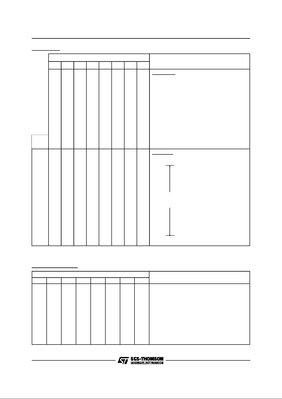
Bass, Treble
TDA7432
D4
Input
Selector
0
0
1
1
1
1
1
1
1
1
1
1
1
1
1
1
1
1
0
0
MSB LSB
D
D
D
D
D
D
D
7
6
5
4
3
2
0
0
0
0
0
0
0
0
1
0
1
0
1
0
1
0
1
1
1
1
1
1
1
1
0
1
0
1
0
1
0
1
1
0
0
0
0
0
0
0
0
0
0
0
0
0
1
0
1
0
1
0
1
0
1
1
1
1
1
1
1
1
0
1
0
1
0
1
0
1
0
1
0
1
0
0
0
0
1
0
0
1
1
1
0
0
1
0
0
1
1
1
1
1
0
1
1
0
0
0
1
1
0
1
1
0
0
0
0
0
1
0
D
1
0
0
1
0
0
1
1
1
0
0
1
0
0
1
1
1
1
1
0
1
1
0
0
0
1
1
0
1
1
0
0
0
0
Treble Steps
- 14dB
-12dB
-10dB
-8dB
-6dB
-4dB
-2dB
0dB
0dB
+2dB
+4dB
+6dB
+8dB
+10dB
+12dB
+14dB
Bass Steps
-18dB
-16dB
-14dB
-12dB
-10dB
-8dB
-6dB
-4dB
-2dB
0dB
0dB
+2dB
+4dB
+6dB
+8dB
+10dB
+12dB
+14dB
+16dB
+18dB
normal
range
14dB
±
FUNCTION
For example 12dB Treble and -8dB Bass give the followingDATA BYTE: 0 0 1 1 1 0 0 1
Speaker Attenuators
MSB LSB
D
D
7
X
X
D
6
X
X
D
5
0
0
D
4
0
0
D
3
0
0
D
2
0
0
D
1
0
0
0
1
:
X
X
X
X
X
X
X
X
X
X
X
X
X
X
X
X
0
0
0
0
0
0
0
0
1
1
1
1
1
1
1
1
1
1
1
1
1
1
1
1
0
0
0
0
1
1
1
1
0
0
1
1
0
1
1
1
0
1
0
1
0
1
0
1
1
X
X
1
X
X
X
X
X
0
SPEAKER ATTENUATOR LF, LR, RF, RR
0dB
-1dB
:
-24dB
-25.5dB
-27dB
-28.5dB
-30dB
-32dB
-34.5dB
-37.5dB
Speaker Mute
7/10

TDA7432
Loudness
MSB LSB
D
D
7
X
X
X
X
X
X
X
X
X
X
X
X
X
X
X
X
X
D
6
X
X
X
X
X
X
X
X
X
X
X
X
X
X
X
X
X
D
5
X
X
X
X
X
X
X
X
X
X
X
X
X
X
X
X
X
D
4
0
0
0
0
0
0
0
0
0
0
0
0
0
0
0
0
D
1
D
3
0
0
0
0
0
0
0
0
1
1
1
1
1
1
1
1
D
3
D
2
0
0
0
0
1
1
1
1
0
0
0
0
1
1
1
1
D1
2
D
1
0
0
1
1
0
0
1
1
0
0
1
1
0
0
1
1
0
1
0
1
0
1
0
1
0
1
0
1
0
1
0
1
D0
0
0dB
-1dB
-2dB :
-3dB
-4dB
-5dB
-6dB
-7dB
-8dB
-9dB
-10dB
-11dB
-12dB
-13dB
-14dB
-15dB
Loudness flat (Note 3)
LOUDNESS
For example to select -14dBLoudness theData Byte is : XX X 01110.
Note3:
Fiat attenuation, according to the selected byte. The loudnesscan be completely disabled by setting bit D7 in the volume byte to ”0”. In this
case the attenuation is 0dB independent from the loudness settings.
Functional Description
The input selector is able to select 1 stereoinputs
and 1 mono input (AM). The inputs are DC biased
with 100kΩ resistorsto the internal reference voltage of 3V. The AM input can be use additionally
as hardware mute pin. If this pin is pulled to
ground by an external transistorandAM is not selected, the input selector mutes the input (reference voltage selected). The AM part is considered to be switched OFF. If the output of the AM
part is not high ohmic in this condition, a series
resistor of about 20kΩhasto be foreseen.
The volume control can be programmed from a
gain of +32dB to an attenuation of -79dB in 1dB
steps. The maximum gain should be kept as low
as possiblefor system performancereason. It has
to be limited by software to the absolute necessary system gain, dependingon the signal source
level and the power amplifier gain.
The bass control acts in a range from +18dB to 18dB in 2dB steps. The filter response is deter-
8/10
mined by the external filter components. An extensive simulationsoftware is available in order to
supportthe design of the bass filter response with
differentfilterconfigurations.
The extended bass boost range of +18dB allows
the implementationof thesoftware loudnessfunction by additionalbass and treble boost.
The treble control acts in a rangeof ±14dB in 2dB
steps. The external capacitor determines with the
internal resistor of 50KΩ the corner frequencyof
the treble response.
The four speakerattenuatorscanbe controlled independentlyfrom 0 to -37.5dB, which allows the
implementation of balance and fader a the four
speaker system. The attenuation steps size is 1
db from 0 to -24dB and increases nonlinearly up
to the maximum attenuation of 37.5dB. A special
mute bit forces the speaker attenuator into the
muteposition.
All 4 outputs are low distortion push pull outputs,
able to drive a load of 3kΩ.

SO20 PACKAGEMECHANICAL DATA
TDA7432
DIM.
MIN. TYP. MAX. MIN. TYP. MAX.
A 2.65 0.104
a1 0.1 0.3 0.004 0.012
a2 2.45 0.096
b 0.35 0.49 0.014 0.019
b1 0.23 0.32 0.009 0.013
C 0.5 0.020
c1 45 (typ.)
D 12.6 13.0 0.496 0.512
E 10 10.65 0.394 0.419
e 1.27 0.050
e3 11.43 0.450
F 7.4 7.6 0.291 0.299
L 0.5 1.27 0.020 0.050
M 0.75 0.030
S 8 (max.)
mm inch
9/10

TDA7432
Information furnished is believed to be accurate and reliable. However, SGS-THOMSON Microelectronicsassumes no responsability for the
consequences of use of such information nor for any infringement of patents or otherrights of third parties which may results from its use. No
license is granted by implication or otherwise under any patent or patent rights of SGS-THOMSON Microelectronics. Specifications mentioned in this publication are subject to change without notice. This publication supersedes and replaces all information previously supplied.
SGS-THOMSON Microelectronics products are not authorized for use as critical components in life support devices or systems without express written approval of SGS-THOMSON Microelectronics.
1996 SGS-THOMSONMicroelectronics - Printed in Italy- All Rights Reserved
SGS-THOMSON Microelectronics GROUP OF COMPANIES
Australia- Brazil - France - Germany - Hong Kong- Italy- Japan - Korea - Malaysia - Malta- Morocco - The Netherlands -
Singapore - Spain - Sweden - Switzerland - Taiwan - UnitedKingdom - U.S.A.
10/10
 Loading...