

TDA7429S
DIGITALLY CONTROLLED AUDIO PROCESSOR
WITH SURROUND SOUND MATRIX
3 STEREO/4STEREOINPUTS
INPUT ATTENUATION CONTROL IN 0.5dB
STEP
TREBLEMIDDLE AND BASS CONTROL
THREE SURROUND MODES ARE AVAIL-
ABLE:
- MUSIC: 4 SELECTABLERESPONSES
- MOVIE ANDSIMULATED:
256SELECTABLE RESPONSES
FOURSPEAKERS ATTENUATORS:
- 4 INDEPENDENTSPEAKERSCONTROL
IN 1dB STEPSFORBALANCE FACILITY
- INDEPENDENTMUTE FUNCTION
ALL FUNCTIONS PROGRAMMABLE VIA SERIAL BUS
DESCRIPTION
The TDA7429 is volume tone (bass middle and
treble) balance (Left/Right) processors for quality
audio applicationsin TV and Hi-Fisystems.
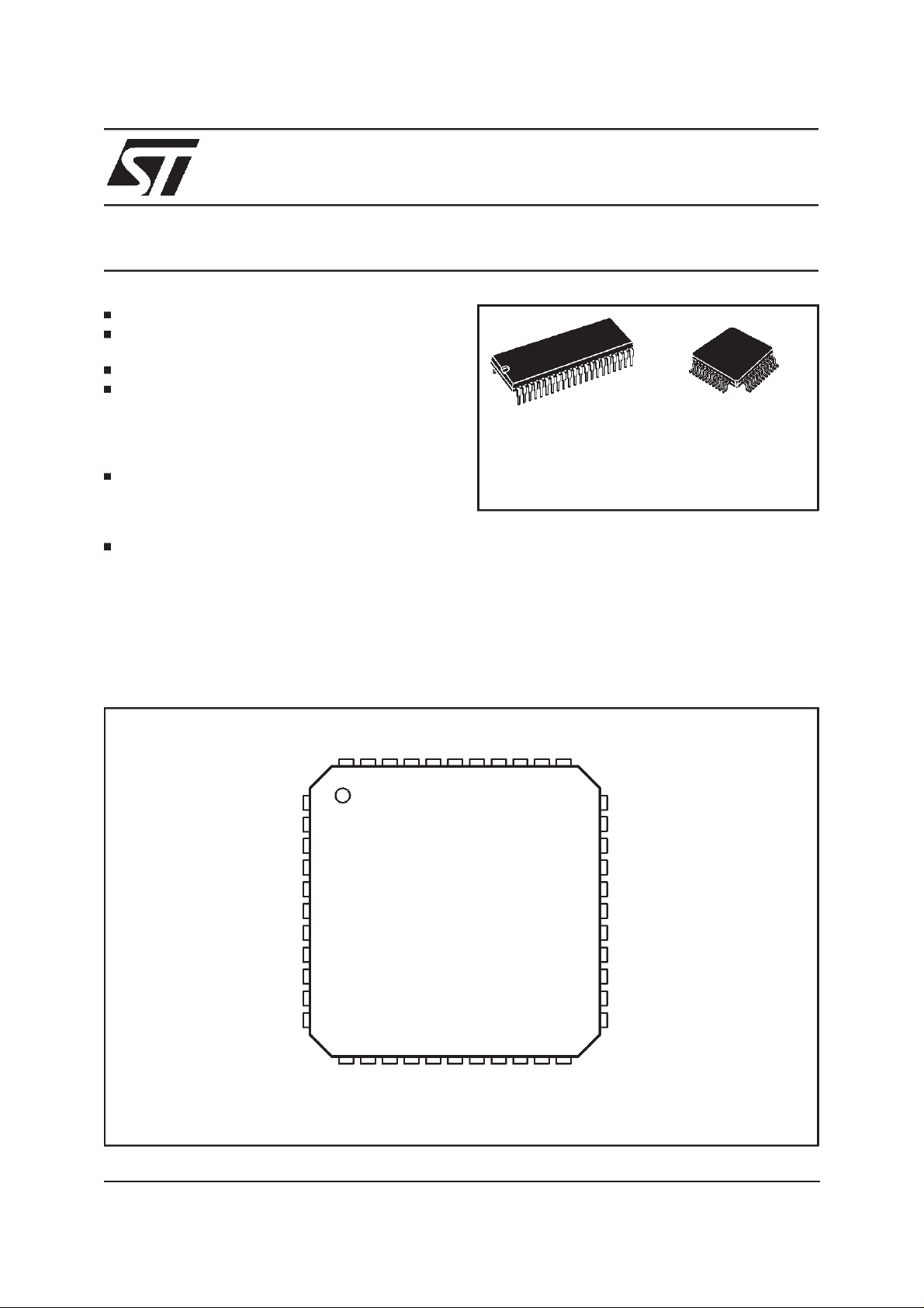
TDA7429T
SDIP42 TQFP44
ORDERING NUMBERS:
TDA7429S TDA7429T
It reproduces surround sound by using programmable phase shifters and a signalmatrix. Control
of all the functionsis accomplishedby serial bus.
The AC signal setting is obtainedby resistor networks and switches combined with operational
amplifiers.
Thanks to theused BIPOLAR/CMOSTechnology,
Low Distortion, Low Noise and DC stepping are
obtained.
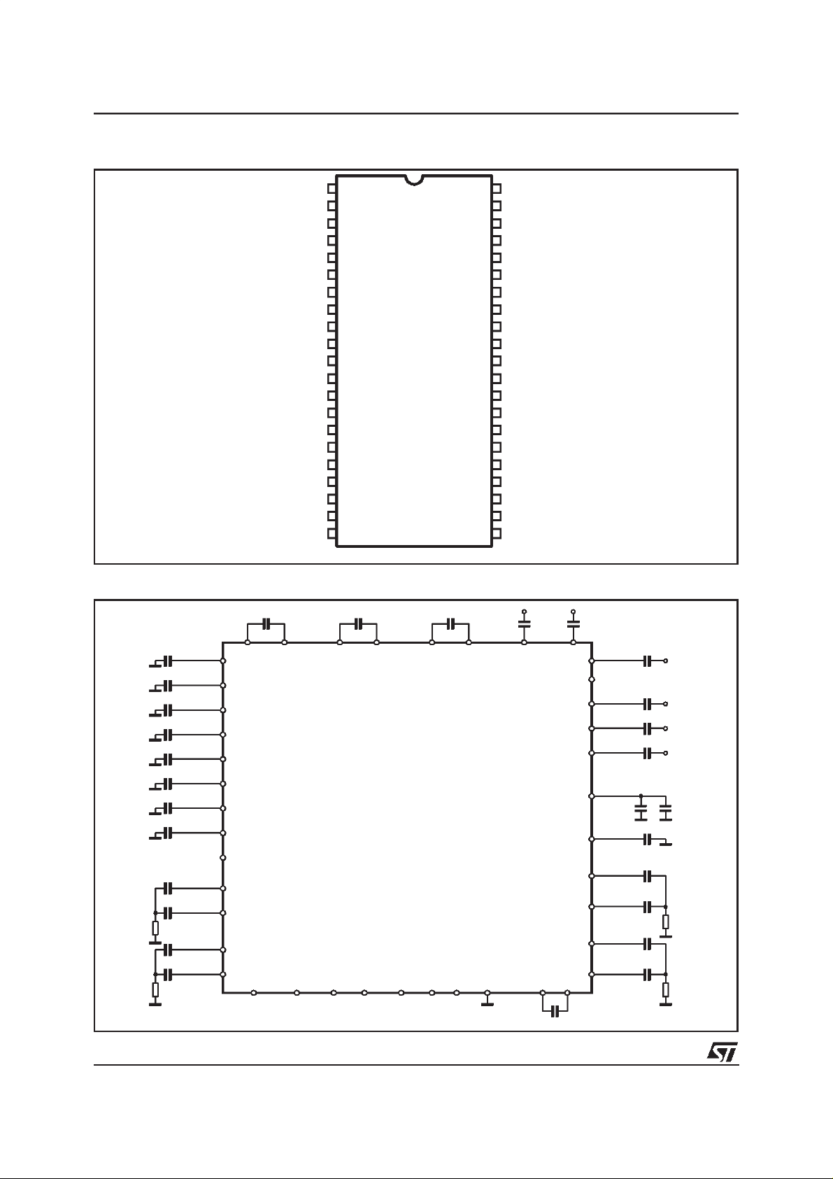
PIN CONNECTION (TQFP44)
LP1
HP1
HP2.
REAROUT
REARIN
VAR_L
BASSO_L
VAR_R
BASSO_R
BASS_LO
BASS_LI
LP
PS1
PS2
44 43 42 41 3940 38 37 36 35 34
1
2
3
4
5
6
7
8
9
10
12 13 14 15 16
BASS_RI
BASS_RO
MIDDLE_LO
S
PS3
V
PS4
CREF
171118 19 20 21 22
MIDDLE_LI
TREBLE_R
MIDDLE_RI
MIDDLE_RO
R_IN4
TREBLE_L
R_IN3
AGND
R_IN2
SDA
R_IN1
33
32
31
30
29
28
27
26
25
24
23
SCL
MONITOR_R
MONITOR_L
L_IN1
L_IN2
L_IN3
L_IN4
AUXOUT_L
AUXOUT_R
L_OUT
R_OUT
DIG_GND
D96AU532
July 1999
1/20
TDA7429S - TDA7429T
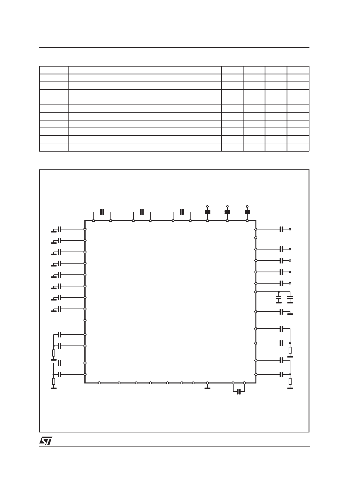
PIN CONNECTION (SDIP42)
REAROUT
MIDDLE_LO
MIDDLE_LI
MIDDLE_RO
TEST CIRCUIT (TDA7429S)
PS4
PS3
PS2
PS1
LP
LP1
HP1
HP2
REARIN
VAR_L
BASSO_L
VAR_R
BASSO_R
BASS_LO
BASS_LI
BASS_RO
BASS_RI
1
2
3
4
5
6
7
8
9
10
11
12
13
14
15
16
17
18
19
20
21
D97AU623
42
41
40
39
38
37
36
35
34
33
32
31
30
29
28
27
26
25
24
23
22
V
S
CREF
R_IN3
R_IN2
R_IN1
MONITOR_R
MONITOR_L
L_IN1
L_IN2
L_IN3
AUXOUT_L
AUXOUT_R
L_OUT
R_OUT
DIG_GND
SCL
SDA
AGND
TREBLE_L
TREBLE_R
MIDDLE_RI
2.7K
2.7K
22nF
22nF
4.7nF
100nF
1.2nF
5.6nF
5.6nF
5.6nF
100nF
22nF
18nF
22nF
18nF
PS4
PS3
PS2
PS1
LP1
TREBLE_R
TREBLE_L
MONITOR_R
MIDDLE_LO
MIDDLE_LI
MIDDLE_RO
MIDDLE_RI
D97AU626
2.2µF
14
1
2
3
4
LP
5
6
23
24
37
19
20
21
22
32 31 30 29 28 27 26 25
AUXOUT_L AUXOUT_R L_OUT R_OUT
BASSO_LVAR_RBASSO_R
13 12 11
2.2µF
VAR_L
REAROUT
DIG_GND SCL SDA AGND
2.2µF
0.47µF
REARIN
910
R_IN3
40 39
0.47µF
87
HP2
R_IN2
HP1
680nF
38
35
34
33
42
41
15
16
17
18
R_IN1
MONITOR_L36
L_IN1
L_IN2
L_IN3
V
S
CREF
BASS_LO
BASS_LI
BASS_RO
BASS_RI
0.47µF
0.47µF
0.47µF
0.47µF
100nF10µF
22µF
220nF
100nF
100nF
5.6K
100nF
100nF
5.6K
2/20
TDA7429S - TDA7429T
QUICK REFERENCEDATA
Symbol Parameter Min. Typ. Max. Unit
V
V
CL
THD Total Harmonic DistortionV = 1Vrms f = 1KHz 0.01 0.1 %
S/N Signal to NoiseRatio V
S
TEST CIRCUIT (TDA7429T)
Supply Voltage 7 9 10.2 V
S
Max. input signal handling 2 Vrms
= 1Vrms (mode = OFF) 106 dB
out
Channel Separation f= 1KHz 90 dB
C
Treble Control (2db step) -14 +14 dB
Middle Control (2dbstep) -14 +14 dB
Bass Control (2dB step) -14 +14 dB
Balance Control 1dB step (L
CH, RCH) -79 0 dB
Mute Attenuation 100 dB
2.7K
2.7K
22nF
22nF
4.7nF
100nF
1.2nF
5.6nF
5.6nF
5.6nF
100nF
22nF
18nF
22nF
18nF
PS4
PS3
PS2
PS1
LP1
TREBLE-R
TREBLE-L
MONITOR_R
MIDDLE-LO
MIDDLE-LI
MIDDLE-RO
MIDDLE-RI
D96AU533
2.2µF
BASSO-LVAR-RBASSO-R
9
40
41
42
43
LP
44
1
18
19
33
14
15
16
17
AUXOUT-L AUXOUT-R L-OUT R-OUT
876
27 26 25 24 23 22 21 20
2.2µF
VAR-L
2.2µF
0.47µF
REAROUT
REARIN
45
R-IN4
TDA7429
DIG-GND SCL SDA AGND
0.47µF
R-IN3
37 36 35
32
HP2
0.47µF
R-IN2
HP1
680nF
R-IN1
34
MONITOR_L32
L-IN1
31
L-IN2
30
L-IN3
29
L-IN4
28
V
39
CREF
38
10
BASS-LO
11
BASS-LI
BASS-RO
12
13
BASS-RI
0.47µF
0.47µF
0.47µF
0.47µF
0.47µF
S
100nF10µF
22µF
220nF
100nF
100nF
5.6K
100nF
100nF
5.6K
3/20
TDA7429S - TDA7429T
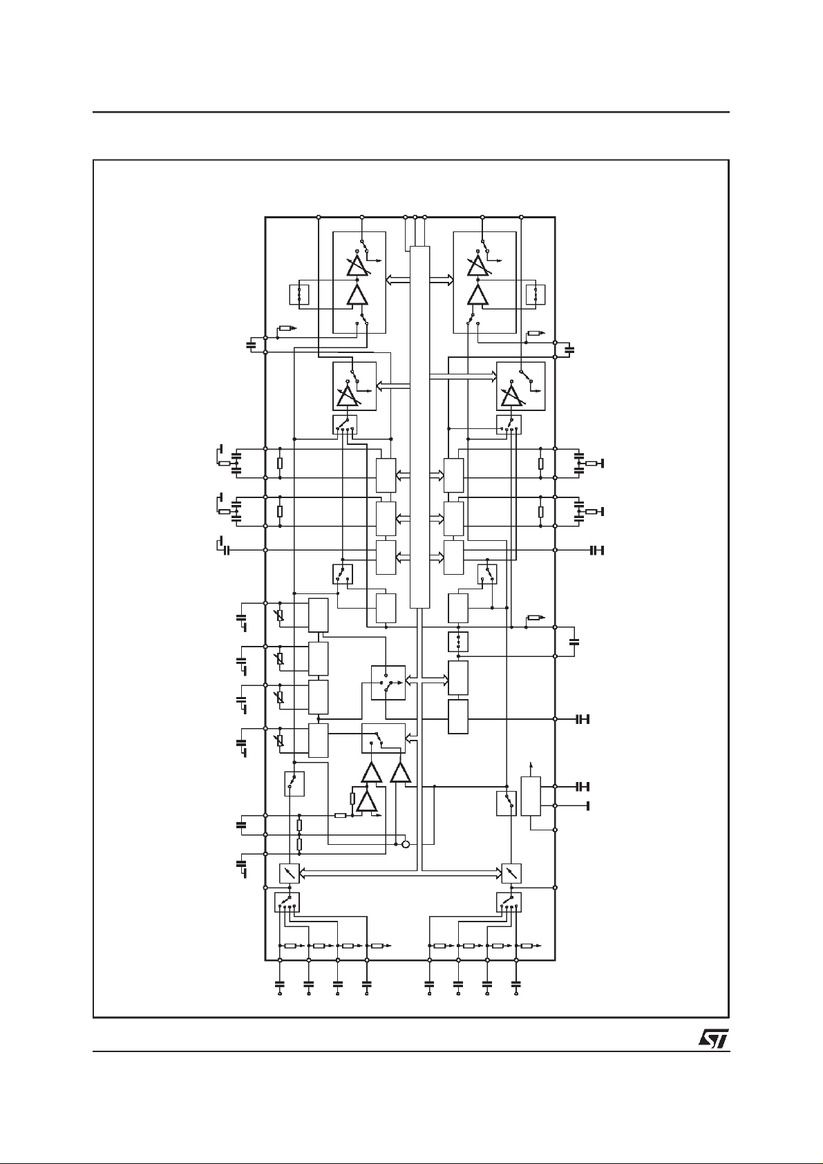
BLOCK DIAGRAM (TDA7429T)
AUXOUT-L
27
SPKR
79dB CONTROL
SCL
SDA
L-OUT
25
ATT
MUTE
DIG GND
222123
SPKR
R-OUT
AUXOUT-R
24
26
ATT
MUTE
79dB CONTROL
D96AU513
5.6K
2.7K
100nF
100nF
22nF
18nF
5.6nF
22nF
22nF
4.7nF
100nF
5.6nF 680nF
2.2µF
BASSO-L VAR-L
BASS-LO
10 7 6
BASS-LI
MIDDLE-LO
MIDDLE-LI
15 14 11
19
TREBLE-L
PS4
PS3
PS2
PS1
LP1 HP1 HP2
1 2 3 43 42 41 40
31.5dB
control
32
MONITOR L
30K
FIX
RB
RM
RPS4
RPS3
RPS2
RPS1
RHP1
RLP1
PS4
PS3
PS2
PS1
79dB CONTROL
OFF
400Hz
400Hz
4KHz
90Hz
REC
SURR
R5
-
+
FIX
VAR
ATT
MUTE
3BAND
C BUS DECODER + LATCHES
2
BASS
MIDDLE
TREBLE
AMP
MIXING
MOVIE/SIM
MUSIC
MOVIE/
I
OFF
L-R
-
+
+
REAR
SURR
MUSIC
SIM
-
+
R6
-
+
FIX
FIX
TREBLE MIDDLE BASS
AMP
MIXING
EFFECT
CONTROL
LPF
9KHz
+
VAR
SURR
-
30K
89121833
2.2µF
ATT
REC
MUTE
BASSO-R VAR-R
79dB CONTROL
3BAND
BASS-RO
SURR
REAR
RM RB
17 16 13
OFF
50K
45
Vref
SUPPLY
39 20 38 44
31.5dB
control
TREBLE-R
LP
CREF
AGND
S
V
MONITOR R
BASS-RI
100nF 100nF
MIDDLE-RO
18nF 22nF
MIDDLE-RI
REARIN
2.2µF
REAROUT
1.2nF
22µF
5.6K
2.7K
5.6nF
4/20
50K
50K
50K
L-IN3
50K
28
L-IN4
0.47µF
31
30
29
L-IN1
L-IN2
0.47µF
0.47µF
0.47µF
50K
34
35
R-IN2
R-IN1
0.47µF
0.47µF
37
36
R-IN4
R-IN3
0.47µF
0.47µF
THE SWITCHES POSITION MATCHES THE RESET CONDITION
50K
50K
50K
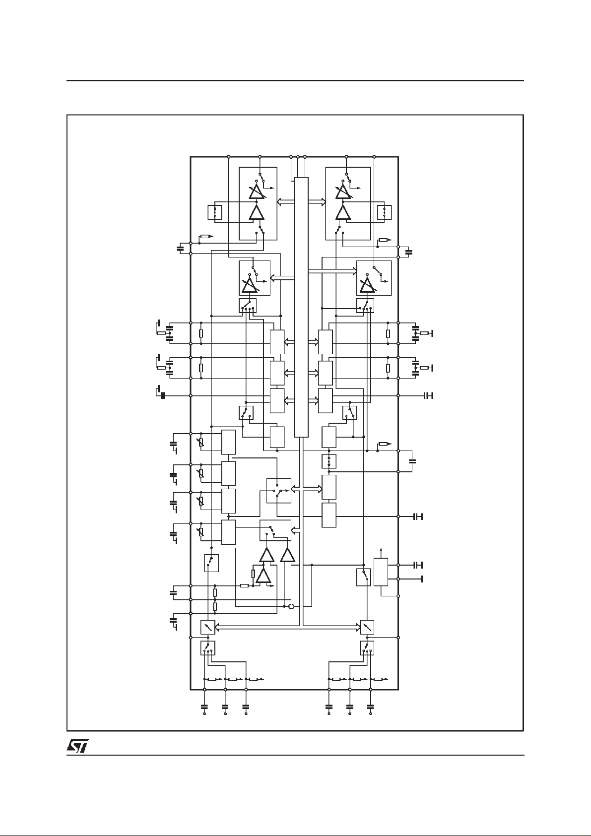
BLOCK DIAGRAM (TDA7429S)
AUXOUT_L
32
SPKR
79dB CONTROL
TDA7429S - TDA7429T
SCL
SDA
L_OUT
30
ATT
MUTE
DIG GND
272628
SPKR
R_OUT
AUXOUT_R
29
31
ATT
MUTE
79dB CONTROL
D97AU624A
5.6K
2.7K
100nF
100nF
22nF
18nF
5.6nF
22nF
22nF
4.7nF
100nF
5.6nF 680nF
30K
2.2µF
BASSO_L VAR_L
BASS_LO
15 12 11
RB
BASS_LI
MIDDLE_LO
RM
MIDDLE_LI
20 19 16
24
TREBLE_L
PS4
RPS4
PS3
RPS3
PS2
RPS2
PS1
RPS1
LP1 HP1 HP2
678 4321
31.5dB
control
36
MONITOR_L
-
+
FIX
VAR
ATT
REC
MUTE
79dB CONTROL
FIX
SURR
OFF
PS4
400Hz
PS3
400Hz
PS2
4KHz
PS1
90Hz
R5
RHP1
RLP1
3BAND
C BUS DECODER + LATCHES
2
BASS
MIDDLE
TREBLE
AMP
MIXING
MOVIE/SIM
MUSIC
MOVIE/
I
OFF
L-R
-
+
+
REAR
SURR
MUSIC
SIM
-
+
R6
-
+
FIX
FIX
TREBLE MIDDLE BASS
AMP
MIXING
EFFECT
CONTROL
LPF
9KHz
+
VAR
SURR
-
30K
1314172337
2.2µF
ATT
REC
MUTE
BASSO_R VAR_R
79dB CONTROL
3BAND
BASS_RO
REAR
SURR
RM RB
22 21 18
OFF
50K
910
Vref
SUPPLY
42 25 41 5
31.5dB
control
BASS_RI
TREBLE_R
REARIN
1.2nF
LP
22µF
CREF
AGND
S
V
MONITOR_R
5.6K
100nF 100nF
MIDDLE_RO
2.7K
18nF 22nF
MIDDLE_RI
5.6nF
2.2µF
REAROUT
50K
50K
L_IN2
50K
33
L_IN3
0.47µF
35
34
L_IN1
0.47µF
0.47µF
50K
38
R_IN1
0.47µF
40
39
R_IN3
R_IN2
0.47µF
0.47µF
THE SWITCHES POSITION MATCHES THE RESET CONDITION
50K
50K
5/20
TDA7429S - TDA7429T
THERMAL DATA
Symbol Description Value Unit
R
thj-pins
ABSOLUTE MAXIMUM RATINGS
Symbol Parameter Value Unit
V
T
amb
T
Thermal Resistance Junction-pins Max. 85
Operating Supply Voltage 11 V
S
Operating Ambient Temperature -10 to 85
Storage Temperature Range -55 to +150
stg
C/W
°
°
°
C
C
ELECTRICALCHARACTERISTICS (refer to the testcircuit T
V
= 1Vrms;RG= 600Ω, all controlsflat (G = 0dB), EffectCtrl = -6dB, MODE = OFF;f = 1KHz
in
=25°C, VS= 9V, RL= 10KΩ,
amb
unless otherwisespecified)
Symbol Parameter Test Condition Min. Typ. Max. Unit
SUPPLY
V
S
I
S
SVR Ripple Rejection L
Supply Voltage 7 9 10.2 V
Supply Current 10 18 26 mA
CH/RCH out
, Mode = OFF 60 80 dB
INPUTSTAGE
C
RANGE
A
A
A
R
IN
V
CL
VMIN
VMAX
STEP
Input Resistance 35 50 65 K
Clipping Level THD = 0.3% 2 2.5 Vrms
Control Range 31.5 dB
Min. Attenuation -1 0 1 dB
Max. Attenuation 31 31.5 32 dB
Step Resolution 0.5 1 dB
BASSCONTROL
Gb Control Range Max. Boost/cut +11.5 +14.0 +16.0 dB
B
STEP
R
B
Step Resolution 1 2 3 dB
Internal Feedback Resistance 32 44 56 KΩ
MIDDLE CONTROL
Gm Control Range Max. Boost/cut +11.5 +14.0 +16.0 dB
M
STEP
R
M
Step Resolution 1 2 3 dB
Internal Feedback Resistance 17.5 25 32.5 KΩ
Ω
TREBLECONTROL
Gt ControlRange Max. Boost/cut +13.0 +14.0 +15.0 dB
T
STEP
Step Resolution 1 2 3 dB
EFFECTCONTROL
C
RANGE
S
STEP
Control Range -21 -6 dB
Step Resolution 0.5 1 1.5 dB
SURROUNDSOUND MATRIXPHASE
6/20
R
R
R
R
R
PS10
PS11
PS12
PS13
PS20
Phase Shifter1: D1 = 0, D0 = 0 8.3 11.8 15.2 KΩ
Phase Shifter1: D1 = 0, D0 = 1 10 14.1 18.3 KΩ
Phase Shifter1: D1 = 1, D0 = 0 12.6 17.9 23.3 K
Phase Shifter1: D1 = 1, D0 = 1 26.4 37.3 48.85 KΩ
Phase Shifter2: D3 = 0, D2 = 0 4 5.6 7.2 KΩ
Ω

TDA7429S - TDA7429T
ELECTRICALCHARACTERISTICS
(continued)
SURROUNDSOUND MATRIX
TEST CONDITION(PhaseResistor SelectionD0=0, D1=1, D2=0.D3=1, D4=0,D5=1, D6=0, D7=1
Symbol Parameter Test Condition Min. Typ. Max. Unit
R
PS21
R
PS22
R
PS23
R
PS30
R
PS31
R
PS32
R
PS33
R
PS40
R
PS41
R
PS42
R
PS43
G
OFF
D
GOFF
G
MOV
D
GMOV
G
MUS
D
GMUS
L
MON1
L
MON2
L
MON3
R
MON1
R
MON2
R
MON3
R
LP1
R
HPI
R
LPF
Phase Shifter2: D3 = 0, D2 = 1 4.8 6.8 8.7 KΩ
Phase Shifter2: D3 = 1, D2 = 0 6 8.4 10.9 KΩ
Phase Shifter2: D3 = 1, D2 = 1 12.9 18.3 23.7 KΩ
Phase Shifter3: D5 = 0, D4 = 0 8.5 12.1 15.6 KΩ
Phase Shifter3: D5 = 0, D4 = 1 10.2 14.5 18.7 K
Phase Shifter3: D5 = 1, D4 = 0 12.7 18.1 23.3 KΩ
Phase Shifter3: D5 = 1, D4 = 1 27.4 39.1 50.75 KΩ
Phase Shifter4: D7 = 0, D6 = 0 8.5 12.1 15.6 KΩ
Phase Shifter4: D7 = 0, D6 = 1 10.2 14.5 18.7 KΩ
Phase Shifter4: D7 = 1, D6 = 0 12.7 18.1 23.3 K
Phase Shifter4: D7 = 1, D6 = 1 27.4 39.1 50.75 K
In-phase Gain (OFF) Mode OFF, Input signal of
LR In-phase Gain Difference
(OFF)
1kHz, 1.4 V
Lin→ L
out
Mode OFF, Input signal of
1kHz, 1.4 V
Rin→ R
out,Lin
p-p,Rin
p-p
→ L
→ R
out
out
In-phase Gain (Movie) Movie mode, Effect Ctrl = -6dB
LR In-phase Gain Difference
(Movie)
Input signal of 1kHz, 1.4 V
Rin→ R
out,Lin
→ L
Movie mode, Effect Ctrl = -6dB
Input signal of 1kHz, 1.4 V
(Rin→ R
)–(Lin→ L
out
out
out
p-p
p-p
)
In-phase Gain (Music) Musicmode, Effect Ctrl = -6dB
LR In-phase Gain Difference
(Music)
Input signal of 1kHz, 1.4 V
R
(R
in
→
out
), (L
→
in
Music mode, Effect Ctrl = -6dB
Input signal of 1kHz, 1.4 V
(Rin→ R
)-(Lin→ L
out
p-p
L
)
out
p-p
)
out
Simulated L Output 1 SimulatedMode,EffectCtrl= -6dB
-1 0 1 dB
-1 0 1 dB
8dB
0dB
7dB
0dB
4.5 dB
Input signal of 250Hz,
1.4 V
Simulated L Output 2 SimulatedMode,EffectCtrl= -6dB
p-p,Rin
and Lin→ L
out
–4.0 dB
Input signal of 1kHz,
1.4 V
Simulated L Output 3 SimulatedMode, EffectCtrl= -6dB
p-p,Rin
and Lin→ L
out
7.0 dB
Input signal of 3.6kHz,
1.4 V
p-p,Rin
and L
Simulated R Output 1 SimulatedMode,EffectCtrl= -6dB
L
→
in
out
– 4.5 dB
Input signal of 250Hz,
1.4 V
Simulated R Output 2 SimulatedMode,EffectCtrl= -6dB
p-p,Rin
and Lin→R
out
3.8 dB
Input signal of 1kHz,
1.4 V
Simulated R Output 3 SimulatedMode,EffectCtrl= -6dB
p-p,Rin
and Lin→R
out
–20 dB
Input signal of 3.6kHz,
1.4 V
p-p,Rin
and Lin→ R
out
Low Pass FilterResistance 7 10 13 KΩ
High Pass FilterResistance 42 60 78 KΩ
LP PinImpedance 7 10 13 K
Ω
Ω
Ω
Ω
7/20

TDA7429S - TDA7429T
ELECTRICALCHARACTERISTICS (continued)
Symbol Parameter Test Condition Min. Typ. Max. Unit
SPEAKER & AUXATTENUATORS
C
range
S
STEP
E
A
V
DC
A
MUTE
R
VEA
AUDIOOUTPUTS
N
O(OFF)
N
O(MOV)
N
O(MUS)
N
O(MON)
d Distorsion Av = 0; V
S
C
V
OCL
R
OUT
V
OUT
MONITOROUTPUTS
d Distorsion Av = 0; Vin= 1Vrms 0.01 0.1 %
S
C
V
OCL
R
OUT
V
OUT
BUS INPUTS
V
IL
V
IH
I
IN
V
O
Control Range 79 dB
Step Resolution -0.5 1 1.5 dB
Attenuation set error Av = 0 to -20dB -1.5 0 1.5 dB
Av = -20to -79dB -3 0 2 dB
DC Steps adjacent att. steps -3 0 3 mV
Output Mute Condition +70 100 dB
Input Impedance 21 30 39 KΩ
Output Noise(OFF) Output Mute, Flat
B
= 20Hz to 20KHz
W
Output Noise(Movie) Mode =Movie ,
B
= 20Hz to 20KHz
W
Output Noise(Music) Mode = Music ,
B
= 20Hz to 20KHz,
W
Output Noise(Simulated) Mode = Simulated,
B
= 20Hz to 20KHz
W
= 1Vrms 0.01 0.1 %
in
4
5
30 µVrms
30 mVrms
30 µVrms
Channel Separation 70 90 dB
Clipping Level d = 0.3% 2 2.5 Vrms
Output Resistance 25 50 85 Ω
DC Voltage Level 3.8 V
Channel Separation 70 90 dB
Clipping Level d = 0.3% 2 2.5 Vrms
Output Resistance 25 50 85 Ω
DC Voltage Level 4.5 V
Input Low Voltage 1V
Input High Voltage 3 V
Input Current -5 +5
Output VoltageSDA
IO= 1.6mA 0.4 V
Acknowledge
µVrms
µVrms
A
µ
8/20

TDA7429S - TDA7429T
2
C BUS INTERFACE
I
Data transmission from microprocessor to the
TDA7429 and viceversa takes place through the
2 wires I
2
C BUS interface, consisting of the two
lines SDA and SCL (pull-up resistors to positive
supply voltage must be connected).
Data Validity
As shown in fig. 3, the data on the SDA line must
be stable during the high period of theclock. The
HIGH and LOW state of the data line can only
change when the clock signal on the SCL line is
LOW.
Start and StopConditions
As shown in fig.4 a start condition is a HIGH to
LOW transition of the SDA line while SCL is
HIGH. The stop condition is a LOW to HIGHtransition of the SDAline while SCL is HIGH.
Byte Format
Every byte transferred on the SDA line must con-
tain 8 bits. Each byte must be followed by an ac-
Figure 3:
Data Validityon theI
2
CBUS
knowledgebit. The MSB is transferredfirst.
Acknowledge
The master (µP)puts a resistiveHIGH level on the
SDA line during the acknowledgeclock pulse (see
fig. 5). The peripheral (audioprocessor) that acknowledges has to pull-down (LOW) the SDA line
duringthisclock pulse.
The audioprocessor which has been addressed
has to generate an acknowledge after the reception of each byte, otherwise the SDA line remains
at the HIGH level during the ninth clock pulse
time. In this case the master transmitter can generate the STOP information in order to abort the
transfer.
Transmission withoutAcknowledge
Avoiding to detect the acknowledge of the audio-
processor,the µP can use a simplertransmission:
simply it waits one clock without checking the
slaveacknowledging, and sends the new data.
This approach of course is less protected from
misworking.
Figure 4:
TimingDiagram of I
2
Figure 5: Acknowledgeon theI
CBUS
2
CBUS
9/20

TDA7429S - TDA7429T
SOFTWARESPECIFICATION
InterfaceProtocol
The interfaceprotocol comprises:
A startcondition (S)
address
A subaddressbytes
A sequenceof data (N byte + achnowledge)
A stopcondition (P)
A chip address byte, containing the TDA7429
CHIP ADDRESS
MSB LSB MSB LSB MSB LSB
S100000A0ACK ACK DATA ACK P
D95AU226A
SUBADDRESS DATA 1 to DATA n
B DATA
ACK = Achnowledge
S = Start
P = Stop
A = Address
B = Auto Increment
EXAMPLES
No IncrementalBus
The TDA7429 receives a start condition, the cor-
rect chipaddress, a subaddresswith the MSB = 0
(no incremental bus), N-datas (all these datas
concern the subaddress selected), a stop condition.
CHIP ADDRESS
MSB LSB MSB LSB MSB LSB
S100000A0ACK ACK DATA ACK P
D95AU306
IncrementalBus
The TDA7429receive s a startcondition, the correct chip address,a subaddresswith theMSB = 1
(incremental bus): now it is in a loop condition
with an autoincrease of the subaddress whereas
CHIP ADDRESS
MSB LSB MSB LSB MSB LSB
S100000A0ACK ACK DATA ACK P
D95AU307
SUBADDRESS DATA
0D3
X X X D2 D1 D0
SUBADDRESS from ”1XXX1010” to ”1XXX1111”
of DATAare ignored.
The DATA 1 concern thesubaddress sent, and
the DATA 2 concern the subaddress sent plus
one in the loop etc, and at the end it receivers the
stop condition.
SUBADDRESS DATA 1 to DATA n
1D3
X X X D2 D1 D0
10/20

TDA7429S - TDA7429T
DATA BYTES
Address = 80(HEX)
FUNCTIONSELECTION:
The first byte (subaddress)
MSB LSB SUBADDRESS
D7 D6 D5 D4 D3 D2 D1 D0
B X X X 0 0 0 0 INPUT ATTENUATION
B X X X 0 0 0 1 SURROUND & OUT & EFFECT
B X X X 0 0 1 0 PHASE RESISTOR
B X X X 0 0 1 1 BASS& NATURAL BASE
B X X X 0 1 0 0 MIDDLE & TREBLE
B X X X 0 1 0 1 SPEAKERATTENUATION ”L”
B X X X 0 1 1 0 SPEAKERATTENUATION ”R”
B X X X 0 1 1 1 AUX ATTENUATION ”L”
B X X X 1 0 0 0 AUX ATTENUATION”R”
B X X X 1 0 0 1 INPUT MULTIPLEXER, & AUX
B = 1 incrementalbus; active
B = 0 no incrementalbus;
X = indifferent 0,1
CONTROL
OUT
INPUT ATTENUATION SELECTION
MSB LSB INPUT ATTENUATION
D7 D6 D5 D4 D3 D2 D1 D0 0.5 dB STEPS
X 000 0
X 0 0 1 -0.5
X 010 -1
X 0 1 1 -1.5
X 100 -2
X 1 0 1 -2.5
X 110 -3
X 1 1 1 -3.5
4 dB STEPS
X 000 0
X 001 -4
X 010 -8
X 011 -12
X 100 -16
X 101 -20
X 110 -24
X 111 -28
INPUT ATTENUATION = 0∼ -31.5dB
D7 D6 D5 D4 D3 D2 D1 D0 REAR SWITCH
X0 REARIN, REAROUT PIN
X1 NO REARIN,REAROUT PIN
ACTIVE
11/20

TDA7429S - TDA7429T
SURROUNDSELECTION
MSB LSB
D7 D6 D5 D4 D3 D2 D1 D0 SURROUND MODE
X 0 0 SIMULATED
X 0 1 MUSIC
X 1 0 OFF
X 1 1 MOVIE
OUT
X 0 VAR
X 1 FIX
EFFECT CONTROL
X0000 -6
X0001 -7
X0010 -8
X0011 -9
X0100 -10
X0101 -11
X0110 -12
X0111 -13
X1000 -14
X1001 -15
X1010 -16
X1011 -17
X1100 -18
X1101 -19
X1110 -20
X1111 -21
PHASE RESISTOR SELECTION
MSB LSB
D7 D6 D5 D4 D3 D2 D1 D0 PHASE SHIFT 1 (KΩ)
00 12
01 14
10 18
11 37
00 6
01 7
10 8
11 18
00 12
01 14
10 18
11 39
00 12
01 14
10 18
11 39
SURROUND PHASE
RESISTOR
PHASE SHIFT 2 (KΩ)
PHASE SHIFT 3 (KΩ)
PHASE SHIFT 4 (KΩ)
12/20

TDA7429S - TDA7429T
BASS SELECTION
MSB LSB BASS
D7 D6 D5 D4 D3 D2 D1 D0 2 dB STEPS
XXX10000 -14
XXX10001 -12
XXX10010 -10
XXX10011 -8
XXX10100 -6
XXX10101 -4
XXX10110 -2
XXX10111 0
XXX11111 0
XXX11110 2
XXX11101 4
XXX11100 6
XXX11011 8
XXX11010 10
XXX11001 12
XXX11000 14
SPEAKER/AUXATT. R & L SELECTION
MSB LSB SPEAKER/AUX ATT
D7 D6 D5 D4 D3 D2 D1 D0 1 dB STEPS
X 000 0
X 001 -1
X 010 -2
X 011 -3
X 100 -4
X 101 -5
X 110 -6
X 111 -7
8 dB STEPS
X0000 0
X0001 -8
X0010 -16
X0011 -24
X0100 -32
X0101 -40
X0110 -48
X0111 -56
X1000 -64
X1001 -72
MUTE
X101X
X11XX
X = INDIFFERENT0,1
SPEAKER/AUXATTENUATION= 0dB
∼
-79dB
13/20

TDA7429S - TDA7429T
MIDDLE& TREBLE SELECTION
MSB LSB MIDDLE
D7 D6 D5 D4 D3 D2 D1 D0 2 dB STEPS
0000 -14
0001 -12
0010 -10
0011 -8
0100 -6
0101 -4
0110 -2
0111 0
1111 0
1110 2
1101 4
1100 6
1011 8
1010 10
1001 12
1000 14
TREBLE
2 dB STEPS
0000 -14
0001 -12
0010 -10
0011 -8
0100 -6
0101 -4
0110 -2
0111 0
1111 0
1110 2
1101 4
1100 6
1011 8
1010 10
1001 12
1000 14
14/20

TDA7429S - TDA7429T
INPUT/RECOUT L & R SELECTION
MSB LSB
D7 D6 D5 D4 D3 D2 D1 D0 INPUT MULTIPLEXER
X 000 IN2
X 010 IN3
X 100 IN4
X 110 IN1
AUX OUT ”L”
X 0 0 0 VER 1 (3BAND)
X 0 1 0 VER 2 (SURR)
X 1 0 0 VER 3 (REAR)
X 1 1 0 FIX
AUX OUT ”R”
X 0 0 0 VER 1 (3BAND)
X 0 1 0 VER 2 (SURR)
X 1 0 0 VER 3 (REAR)
X 1 1 0 FIX
POWER ON RESET
BASS &MIDDLE 2dB
TREBLE 0dB
SURROUND & OUT CONTROL+ EFFECT CONTROL OFF + FIX + MAX ATTENUATION
SPEAKER/AUX ATTENUATION L &R MUTE
INPUT ATTENUATION + REAR SWITCH MAX ATTENUATION + ON
NATURAL BASE OFF
INPUT IN1
PIN: TREBLE-L,TREBLE-R
V
S
25K
GND
D95AU309
20µA
PIN:
VOUTREF
V
S
GND
GND
20µA
D95AU233A
10K
15/20

TDA7429S - TDA7429T
PIN: HP1
LP1
HP2
PIN:
L-IN, R-IN, L-IN2,R-IN2, L-IN3, R-IN3,
V
S
GND
10K
60K
D94AU198
L-IN4, R-IN4,
V
S
PIN: HP2
HP1
PIN:
VAR-L,VAR-R,
V
S
V
GND
S
20µA
5.5K
60K
5.5K
D94AU199
PIN: CREF
V
GND
S
GND
V
REF
20K
20K
50K
42K
20µA
D94AU200
20µA
D95AU336
GND
PIN: LP1
HP1
GND
Vref
30K
V
S
20µA
SW
D95AU227
20µA
10K
D94AU211
16/20

TDA7429S - TDA7429T
PIN:
PIN:
SCL, SDA
REARIN
V
S
GND
20µA
D94AU205
PIN:
PS1, PS2,PS3, PS4, LP
V
S
20µA
GND
D95AU308
PIN:
L-OUT,R-OUT, MONITOR-L, MONITOR-R
REAROUT, BASSO-L,BASSO-R,
AUXOUT_L,AUXOUT_R
V
S
SW
50K
GND
Vref
PIN:
BASS-LI,BASS-RI,MIDDLE- LI,MIDDLE-RI,
V
S
20µA
45K
GND
BASS-LO
BASS-RO,MIDDLE-LO,MIDDLE-RO
or
25K
: Bass
: MIDDLE
20µA
D95AU229
D95AU231A
20µA
GND
D95AU230
PIN:
BASS-LO,BASS-R O,MIDDLE-LO,MIDDLE-RO,
V
S
(*)
GND
BASS-LI,BASS-RI,MIDDLE-LI,MIDDLE-RI
(*) 45K :
Bass
25K : MIDDLE
20µA
D95AU232
17/20

TDA7429S - TDA7429T
DIM.
mm inch
MIN. TYP. MAX. MIN. TYP. MAX.
A 1.60 0.063
A1 0.05 0.15 0.002
0.006
A2 1.35 1.40 1.45 0.053 0.055 0.057
B 0.30 0.37 0.45 0.012 0.014 0.018
C 0.09 0.20 0.004
0.008
D 12.00 0.472
D1 10.00 0.394
D3 8.00 0.315
e 0.80 0.031
E 12.00 0.472
E1 10.00 0.394
E3 8.00 0.315
L 0.45 0.60 0.75 0.018 0.024 0.030
L1 1.00 0.039
K 0°(min.), 3.5°(typ.), 7°(max.)
OUTLINE AND
MECHANICAL DATA
TQFP44 (10 x 10)
D
D1
A1
2333
34
B
44
1
e
11
TQFP4410
22
E
E1
12
L
0.10mm
.004
Seating Plane
B
K
A
A2
C
18/20

TDA7429S - TDA7429T
DIM.
mm inch
MIN. TYP. MAX. MIN. TYP. MAX.
A 5.08 0.20
A1 0.51 0.020
A2 3.05 3.81 4.57 0.120 0.150 0.180
B 0.38 0.46 0.56 0.0149 0.0181 0.0220
B1 0.89 1.02 1.14 0.035 0.040 0.045
c 0.23 0.25 0.38 0.0090 0.0098 0.0150
D 36.58 36.83 37.08 1.440 1.450 1.460
E 15.24 16.00 0.60 0.629
E1 12.70 13.72 14.48 0.50 0.540 0.570
e 1.778 0.070
e1 15.24
e2 18.54
0.60
0.730
e3 1.52 0.060
L 2.54 3.30 3.56 0.10 0.130 0.140
OUTLINE AND
MECHANICAL DATA
SDIP42 (0.600”)
E
E1
A2
A1
LA
BeB1
D
42
1
22
21
c
SDIP42
e1
e2
E
.015
0,38
Gage Plane
e3
e2
19/20

TDA7429S - TDA7429T
Information furnished is believed to be accurate and reliable. However, STMicroelectronics assumes no responsibility for the consequences
of use of such information nor for any infringement of patents or other rights of third parties which may result from its use. No license is
granted by implication or otherwise under any patent or patent rights of STMicroelectronics. Specificationmentioned in this publication are
subject to change withoutnotice. This publication supersedes and replaces all information previously supplied. STMicroelectronics products
are notauthorized for use as criticalcomponents in lifesupport devices or systems without express written approval of STMicroelectronics.
The ST logo is a registered trademark of STMicroelectronics
1999 STMicroelectronics – Printed in Italy – All Rights Reserved
STMicroelectronics GROUP OF COMPANIES
Australia - Brazil - China - Finland - France - Germany- Hong Kong - India - Italy - Japan - Malaysia - Malta - Morocco-
Singapore - Spain - Sweden- Switzerland - UnitedKingdom - U.S.A.
http://www.st.com
20/20
 Loading...