

TDA7427A
AM-FM RADIO FREQUENCY SYNTHESIZER
AND IF COUNTER
ON-CHIP REFERENCE OSCILLATOR AND
PROGRAMMABLEIF COUNTER
VHF INPUT AND PRECOUNTER FOR FREQUENCIES UP TO 290MHz (SUITABLE FOR
DAB APPLICATION)
HF INPUT FOR FREQUENCIES UP TO
64MHz (SHORTWAVE BAND)
IN-LOCK DETECTOR FOR SEARCH/STOP
STATIONFUNCTION
STAND-BY MODE FOR LOW POWER CONSUMPTION
HIGH CURRENT SOURCE FOR 0.5ms
LOCK-INTIME
DIGITAL PORT EXTENSION WITH SIX OUTPUTS FOR FLEXIBILITYIN APPLICATION
FULLY PROGRAMMABLEBYI
2
C BUS
DESCRIPTION
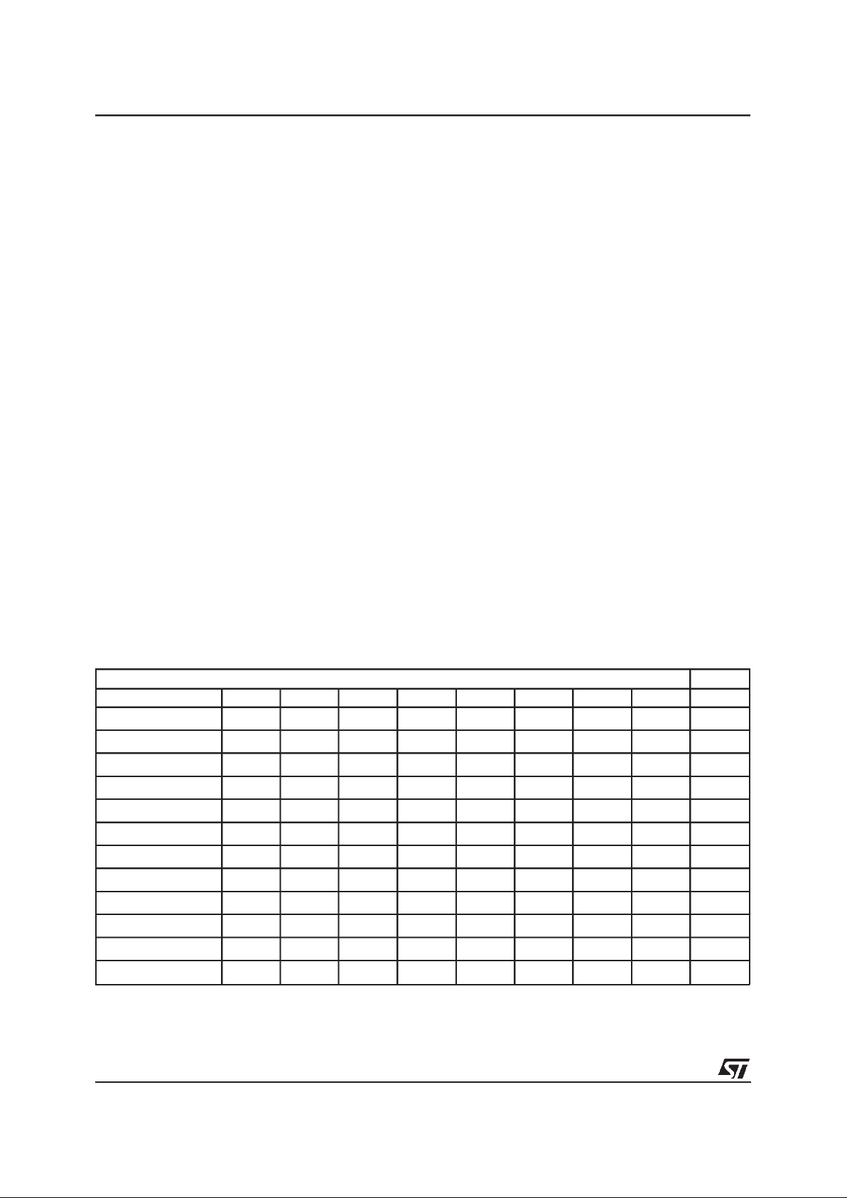
The TDA7427A is a PLL frequency synthesizer
with an additional IF counting system that performs all the functionsneeded in a complete PLL
radio tuning system for conventional and high
speedRDS tuners. The devicehas dedicatedoutputs for IN-LOCK detectionand Search/Stopstation.
July 1998
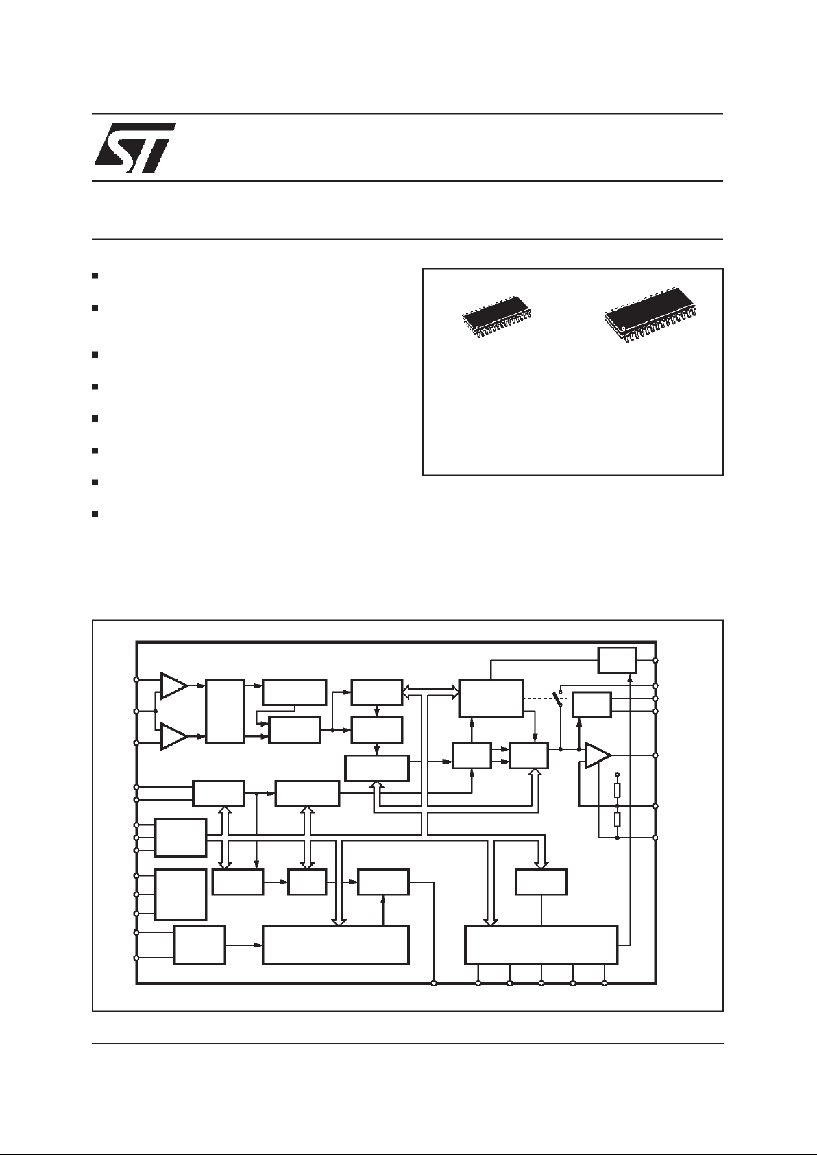
SWITCH
AM/FM
PRECOUNTER
:32/33
5 BIT
PROG.
COUNTER
11-21 BITPROG COUNTER
SWITCH
SWM/DIR
11 BIT
PROG
COUNTER
INLOCK
DETECTOR
PHASE
COMP
REF
OSCILLATOR
CHARGE
PUMP
-
+
SWITCH
LP1/LP2
14 BIT
PROG
COUNTER
TIMER CONTROL
I2C BUS
INTERFACE
TEST
LOGIC
PORT EXTENSION
FM_IN
AM_IN
OSCIN
ADDR
SCL
SDA
IF_AM
IF_FM
DOUT2 DOUT3 DOUT4 DOUT5 DOUT6
VDD2
GNDAN
VREF
LP_OUT
VDD1
LP_FM
LP_AM
D95AU372D
SWITCH
SWM/DIR
16 BIT
PROG
COUNTER
VDD1
OSCOUT
SSTOP
GNDDIG
LP_HC
DOUT1/INLOCK
24
25
9
10
20
12
13
27
21
22
14
15
16 185678
26
4
28
1
3
2
17
HFREF
19
SUPPLY
&
POWER-ON
RESET
SWITCH
AM/FM
SWITCH
OUT
BLOCK DIAGRAM
ORDERING NUMBERS:
TDA7427AAD (TSSOP28)
TDA7427AAD1 (SO28)
TSSOP28
SO28
1/21
ABSOLUTE MAXIMUM RATINGS
Symbol Parameter Value Unit
V
DD1
Supply Voltage - 0.3 to + 7 V
V
DD2
Supply Voltage - 0.3 to+ 11 V
P
tot
Total PowerDissipation 300 mW
T
stg
Storage Temperature - 55 to + 150
o
C
T
amb
Ambient Temperature -40 to + 85
o
C
THERMAL DATA
Symbol Parameter TSSOP28 SO 28 Unit
R
th j-amb
Thermal ResistanceJunction-Ambient 160 65
o
C/W
LP_FM
LP_HC
LP_AM
VREF
DOUT3
DOUT5
DOUT4
DOUT6
OSCIN ADDR
VDD1
GND-DIG
FM_IN
N.C.
AM_IN
GND-AN
VDD2
LPOUT1
3
2
4
5
6
7
8
9
26
25
24
23
22
20
21
19
27
10
28
OSCOUT HFREF
D95AU374C
N.C.
SCL
SDA SSTOP
DOUT1/INLOCK
DOUT211
12
13
18
16
17
1514IF_AM IF_FM
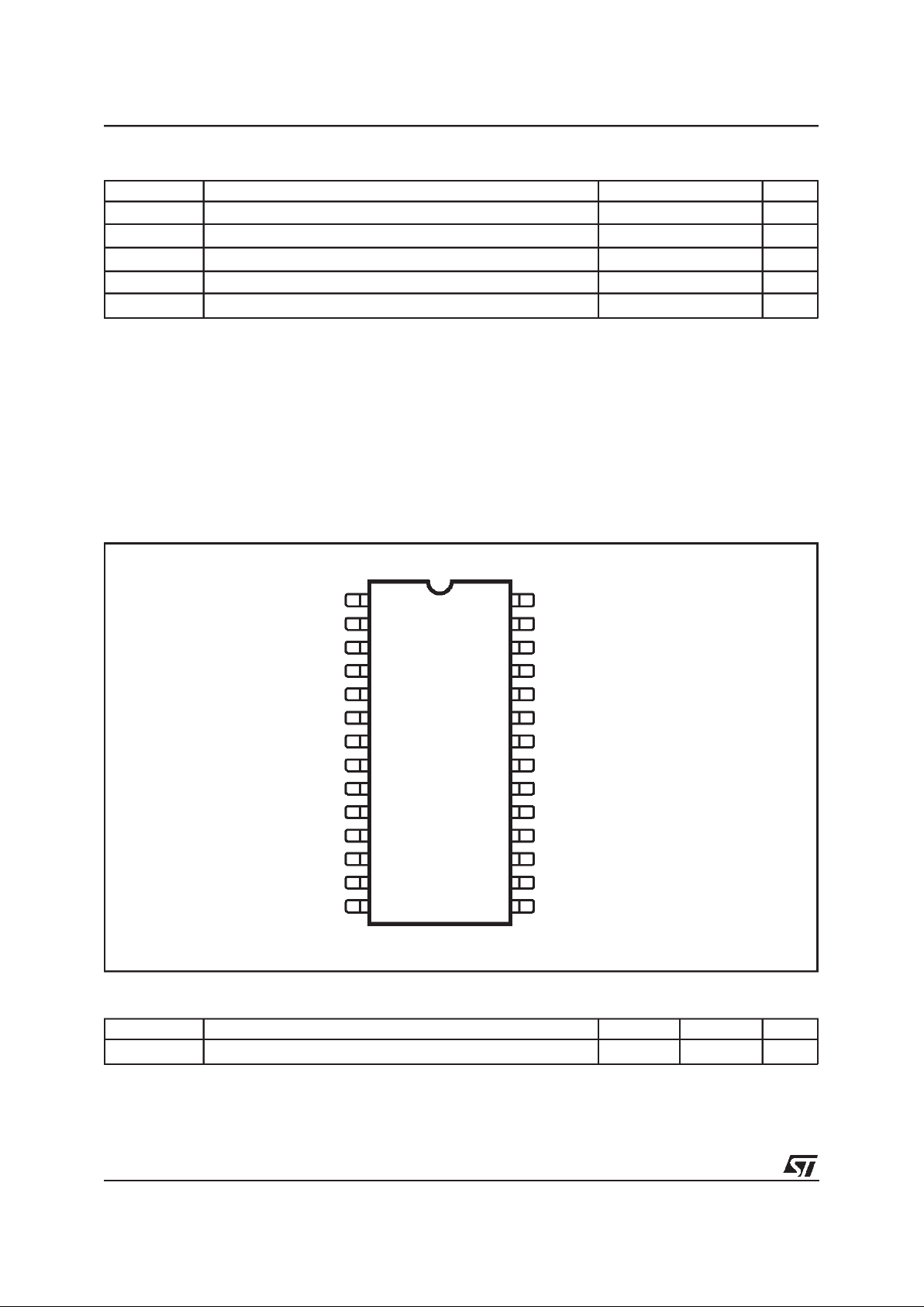
PIN CONNECTION
TDA7427A
2/21

PIN DESCRIPTION
PIN SYMBOL DESCRIPTION
1
LP_FM FilterOPAMP input,charge pump output(FM mode)
2
LP_HC FilterOPAMP input,charge pump output(high current mode)
3
LP_AM FilterOPAMP input, charge pump output(AM mode)
4
VREF OPAMPreference voltage
5
DOUT3 Digital Output 3 (open collector)
6
DOUT4 Digital Output 4 (open collector)
7
DOUT5 Digital Output 5 (open collector)
8
DOUT6 Digital Output 6 (open collector)
9
OSCIN Reference Oscillator Input
10
OSCOUT ReferenceOscillator Output
11
N.C. Not connected
12
SCL I2C bus clock input
13
SDA I2C bus data I/O
14
IF_AM IF counterHF input
15
IF_FM IF counterVHF input
16
SSTOP IF counterresult output
17*
DOUT1 Digital output 1 (push-pull)
17*
INLOCK Inlockdetectoroutput
18
DOUT2 Digital Output 2 (open collector)
19
HF-REF HF reference pin
20
ADDR I2C bus address pin
21
VDD1 Supply Voltage
22
GND-DIG Digitalground
23
N.C. Not connected
24
FM_IN High frequency input FM
25
AM_IN Highfrequencyinput AM
26
GND-AN Analog ground
27
VDD2 Supply Voltage
28
LP_OUT FilterOPAMP output
* Pin function is selectable by software (see softwarespecification)
TDA7427A
3/21
ELECTRICAL CHARACTERISTICS
(T
amb
=25°C; V
DD1
= 5V; V
DD2
= 10V; f
OSC
= 4MHz; unless other-
wise specified).
Symbol Parameter Test Condition Min. Typ. Max. Unit
V
DD1
Supply Voltage 4.5 5.0 5.5 V
V
DD2
Supply Voltage 9.0 11.0 V
I
DD1 Supply Current no output load 2 4 6 mA
I
DD2
Supply Current PLL locked 1 2 3 mA
I
DD1 STB
Supply Current Standby mode 1
µ
A
RF INPUT (AM_IN, FM_IN)
f
iAM
Input Frequency AM Vi = 100mV
rms
sinusoidal 0.5 64 MHz
f
iFM Input Frequency FM Vi = 100mV
rms
sinusoidal 30 200 MHz
V
iMIN
Min Input Voltage AM 0.5 to 16MHz range sinusoidal 30 mVrms
V
iMAX
Max Input Voltage AM 0.6 to 16MHz range sinusoidal 600 mVrms
V
iMIN Min Input Voltage FM 70 to 120MHz range sinusoidal 30 mVrms
V
iMAX
Max Input Voltage FM 70 to 120MHz range sinusoidal 600 mVrms
Z
in Input Impedance FM input 3 4 5 KΩ
Z
in
Input Impedance AM input 3 4 5 KΩ
IF COUNTER (IF_AM, IF_FM)
f
iAM Input Frequency range AM Vi = 100mV
rms
0.400 11 MHz
f
iAM
Input Frequency range FM Vi = 100mV
rms
10 11 MHz
V
iMIN Min Input Voltage AM IF pin f
in
= 455kHz 30 mVrms
V
iMIN
Min Input Voltage FM IF pin fin= 10.7MHz 30 mVrms
V
iMAX
Max Input Voltage AM IF pin fin= 455kHz 600 mVrms
V
iMAX Max Input Voltage FM IF pin f
in
= 10.7MHz 600 mVrms
Z
in
Input Inpedance FM IF pin 3 4 5 KΩ
Z
in Input Inpedance AM IF pin 3 4 5 KΩ
BUS INTERFACE
T
j
Noise Suppression Time
Constant on SCL, SDA Input
50 ns
f
SCL
SCL Clock Frequency 400 kHz
t
AA SCL Low to SDA Data Valid 300 ns
t
buf
Time the bus must be free for
the new transmission
4.7 µs
t
HD-START
START Condition hold time 4.0
µ
s
t
LOW
Clock Low Period 4.7 µs
t
HIGH
Clock High Period 4.0 µs
t
SU-SDA
Start Condition Setup Time 4.7
µ
s
t
HD-DATA Data Input Hold Time 1 µs
t
SU-DATA
Data Input Setup Time 250 ns
t
R SDA & SCL Rise Time 1 µs
t
F
SDA & SCL Full Time 0.3 µs
t
SU-STOP
Stop Condition Setup Time 4.7
µ
s
t
DH DATA OUT Time 300 ns
TDA7427A
4/21
ELECTRICALCHARACTERISTICS
(continued)
Symbol Parameter Test Condition Min. Typ. Max. Unit
V
IL
Input Low Voltage 1V
V
IH Input High Voltage 3 V
I
IN
Input Current -5 +5 µA
V
OUT
Output Voltage SDA
acknowledge
IO= 1.6mA 0.15 0.4 V
OSCILLATOR
t
bu
Build Up Time f
out
= 4MHz 100 ms
C
in
Internal Capacitance 20 pF
C
OUT Internal Capacitance f
osc
= 4MHz 20 pF
Z
in
Input Impedance f
osc
= 4MHz 100 KΩ
V
in Input Voltage (for Slave Mode) f
IN
= 4 to 13MHz (Sinus)
capacitance coupling
300 V
DD
mV
pp
fin Max Input frequency (for Slave
Mode)
VIN= 600mVPP(Sinus) 30 MHz
LOOP FILTER
(LP_FM, LP_AM, LP_HC, LP_OUT)
I
IN
Input Leakage Current (*) VIN= GND; PD
out
= Tristate (1) -1 0.1 1 µA
I
IN
Input Leakage Current (*) VIN=V
DD1
;PD
out
= Tristate (1) -1 0.1 1
µ
A
V
OL
Output Voltage Low IIN= -0.2mA 0 0.5 V
V
OH
Output Voltage High I
OUT
= 0.2mA 9.5 10 V
I
OUT Output Current Sink 10 30 mA
I
OUT
Output Current Source Vout = 0.5 to 9.5V 10 30 mA
DOUT1/SSTOP (push-pull outputs)
V
OL Output Voltage Low I
OUT
= -0.1mA 0.1 0.2 V
V
OH
Output Voltage High I
OUT
= 0.1mA V
DD1
*0.2 4.9 V
DOUT2 to 6
(opencollector outputs)
I
OUT
Output leakage Current V
OUT
= 10V -1 0.1 1 mA
V
OL
Output Voltage Low I
OUT
= -1mA 0.2 0.5 V
I
OUT Output Current Sink Vout = 0.5 to 9.5V 3 5 mA
1) PD = Phase Detector
(*) LP_FM and LP_HC pins only
TDA7427A
5/21
GENERAL DESCRIPTION
This circuit contains a frequency synthesiser and
a loop filter for use in FM/AM radio tuning systems. Only a VCO is required to build a complete
PLL system. For auto search/stopoperationan IF
counter system is available.
For FM and SW AM application, the counter
works in a two-stageconfiguration. The first stage
is a swallow counter with a two modulus (:32/33)
precounter. The second stage is an 11-bit programmable counter.
For LW and MW application,a 16-bit programmable counteris available.
The circuit receivesthe scaling factors for the programmable counters and the values of the reference frequenciesvia a I
2
C bus interface.
The reference frequency is generated by an internal XTAL oscillator followed by the reference divider. The device can operate with XTAL oscillator between 4 and 13MHz either in master mode
and in slave mode.
The reference and step frequencies are free selectable. (XTAL frequency divided by an integer
value). The outputs signals of the phase detector
are switching the programmable current sources.
The loop filter integrates their currents to a DC
voltage.
Values of the current sources are programmable
by 6 bitsalso received via the I
2
C bus.
To minimize the noise induced by the digital part
of the system, a separate power supply supplies
the internal loop filter amplifier. The loop gain can
be set for different conditions by setting the current valuesof thecharge/pumpgenerator.
IF COUNTER SYSTEM
Two separate inputs are available for AM and FM
IF signals. The level of integration is adjustable
by six different measuringcycle times.
The tolerance of the accepted count value is adjustable, to reach an optimum compromise for
searchspeed and precisionof the evaluation.
For the FM range the center frequency of the
measured count value is adjustable in 32 steps,
to get the possibility of fitting the IF filter tolerance. In the AM range an IF frequency of 448 to
479KHz ( 10.684 to 10.715MHz for AM up-conversion)with 1KHz steps is available.
PLL FREQUENCYSYNTHESIZER
InputAmplifiers
The signals applied on AM and FM inputs are amplified to get a logic level in order to drive the frequencydividers.
The typical input impedance for FM and AM inputs is 4kΩ.
MSB LSB
FUNCTION SUBAD BIT 7 BIT 6 BIT 5 BIT 4 BIT 3 BIT 2 BIT 1 BIT 0
PLL CHARGE PUMP
00H LPIN1/2 CURRH B1 B0 A3 A2 A1 A0
PLL COUNTER
01H PC7 PC6 PC5 PC4 PC3 PC2 PC1 PC0
PLL COUNTER
02H PC15 PC14 PC13 PC12 PC11 PC10 PC9 PC8
PLL REF COUNTER
03H RC7 RC6 RC5 RC4 RC3 RC2 RC1 RC0
PLL REF COUNTER
04H RC15 RC14 RC13 RC12 RC11 RC10 RC9 RC8
PLL LOCK DETECT
05H LDENA INLOCK D3 D2 D1 D0 PM1 PM0
IFC REF COUNTER
06H IRC7 IRC6 IRC5 IRC4 IRC3 IRC2 IRC1 IRC0
IFC REF COUNTER
07H IFCM1 IFCM0 IRC13 IRC12 IRC11 IRC10 IRC9 IRC8
IFC CONTROL
08H IFENA - - - - EW2 EW1 EW0
IFC CONTROL
09H IFS2 IFS1 IFS0 CF4 CF3 CF2 CF1 CF0
OSC ADJUST
0AH - - - OSC4 OSC3 OSC2 OSC1 OSC0
PORT EXTENSION
0BH - - DOUT3 DOUT4 DOUT5 DOUT6 DOUT2 DOUT1
Table 1. Address Organization
TDA7427A
6/21
REGISTER NAME FUNCTION
PC
Programmable counter for VCO frequency
RC
Reference counter PLL
IRC
Reference counter IF
IFCM
IF counter mode selector
EW
Frequency error window IF counter
IFENA
Enable IFRC
CF
Center frequency IF counter
IFS
Sampling time IF counter
PM
Stby, FM, AM, AM swallow mode selector
D
Programmable delay and phase error for lock detector
LPIN1/2
Loop filter input select
PLLSTOP
PLL stop
A
Charge pump high current
B
Charge pump low current
LDENA
Lock detector enable
CURRH
Set current high
OSC
Oscillator adjust
DOUT1
Push pull output 5V
DOUT2....6
Open collector output
INLOCK
Lock detector output
Table 2. Control Register Functions.
OSC IN
REGISTER
R0 ...R15
PREDIVIDER
:R
PD
AM IN
FM IN
REGISTER
PC0 ...PC4
COUNTER
A
PRESCALER
M/M+1
REGISTER
PC5 ... P15
COUNTER
:B
fref
fsyn
D95AU375A
∆ϕ
TO CHARGE
PUMP
Figure 1. FM and AM (SW) operation (swallowmode)
TDA7427A
7/21
DIVIDERFROM VCO FREQUENCY TO
REFERENCEFREQUENCY
This divider provides a low frequency f
SYN
which
phase is compared with the reference frequency
f
REF
. It is controlled by the registers PC0 to PC4
and PC5to PC15
OPERATINGMODES
Four operating modes are available fo PLL; they
are user programmable with the Mode PM registers (see table below).
PM0 PM1 Operating Mode
0 0 Standby
1 0 AM (swallow)
0 1 AM (direct)
11 FM
- Standby mode: in this mode all device functions are stopped. This allows low current
consumption without loss of information in all
registers. The pin LP-OUT is forced to 0V,
and all data registers are set to EFH. The oscillatorkeeps running.
- FM and AM (SW) Swallow Mode (SW):
in this mode the FM or AM signal is applied to
a 32/33 prescaler, which is controlled by a 5
bit divider ’A’.The 5 bit register (PC0 to PC4)
controls this divider. In parallel the output of
the prescaler is connected to a 11 bit divider
’B’. (PC5 to PC15).
f
OSC
= (R+1)⋅ f
REF
Dividingrange calculation:
f
VCO
=[33⋅A + (B + 1 - A) ⋅ 32 ] ⋅ f
REF
f
VCO
= (32 ⋅ B + A + 32) ⋅ f
REF
Important:forcorrectoperationA≤32,B≥A,with
AandB variablevaluesofthedividers).
- AM direct mode:
the AM signal is applied directly to the 16 bit static divider ’C’. (PC0 to
PC15)
f
OSC
=(R+1)⋅ fREF
Dividingrange:
f
VCO
=(C+1)⋅ f
REF
THREESTATE PHASE COMPARATOR
The phase comparator generates a phase error
signal according to phase difference between
f
SYN
and f
REF
. This phase error signal drives the
chargepump current generator (fig. 3)
CHARGEPUMP CURRENT GENERATOR
This stage generates signed pulses of current.
The phase error signal decides the duration and
polarityof those pulses.
The current absolutevalues are programmableby
A0, A1, A2 registers for high current and B0, B1,
registersfor low current.
LOWNOISE CMOS OP-AMP
An internal voltage divider at pin VREF connects
the positive input of the low noise Op-Amp. The
charge pump output connects the negative input.
This internal amplifier in cooperationwith external
componentscan providean active filter.
OSC IN
REGISTER
RC0 ... RC15
PREDIVIDER
:R
PHASE
DETECTOR
AM IN
FM IN
REGISTER
PC0 ... PC15
PRESCALER
:C
fref
fsyn
D95AU376A
∆ϕ
TO
CHARGE
PUMP
Figure 2. AM direct mode operation for SW, MW andLW
TDA7427A
8/21

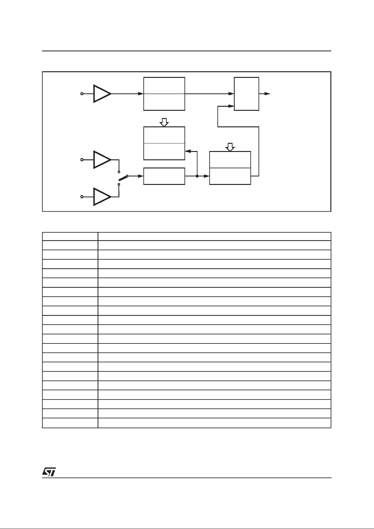
11-21 BIT COUNTER
CF-REGISTER
3 BIT COUNTER14 BIT COUNTER
ZD
IFS-REGISTERIFC-REGISTER
EW-REGISTER
UP/DOWN COUNTER
DECODE SSTOP
IFENA
IF-AM
IF-FM
OSC
D95AU377A
Figure 4. IF Counter internal block diagram
Figure 3. Phase comparator waveforms
TDA7427A
9/21

The negative input is switchable to three input
pins ( LPIN 1, LPIN 2 and LPIN 3) to increasethe
flexibility in application. This feature allows two
separateactive filters for differentapplications
A logical ”1” in the LPIN 1/2 register activates
pin LPIN 1, otherwise pin LPIN 2 is active. While
the high current mode is activated LPIN 3 is
switchedon.
INLOCK DETECTOR
The charge pump can be switched in low current
mode either via software or automatically by the
inlock detector by setting bit LDENA to ”1”.
The charge pump is forced in low current mode
when a phase difference of 10-40 µsec is
reached.
A phase difference larger then the programmed
values will switch the charge pump immediately in
the high current mode.
Programmable delays are available for inlock detection.
IF COUN TERSYSTEM(AM /FM/AM- UPC MODES)
The if counter works in modescontrolled by IFCM
register(see table):
IFCM1 IFCM0 FUNCTION
0 0 NOT USED
0 1 FM MODE
1 0 AM MODE
11
10.7MHz AM UP
CONVERSION MODE
Typical input impedance for IF inputs is 4KΩ.
A sampletimer to generate the gate signal for the
main counter is build with a 14-bit programmable
counter to have the possibility to use any crystal
oscillator frequency. In FM mode 6.25KHz in AM
modea 1KHz signal is generated.This is followed
by an asynchronous divider to generate different
samplingtimes (see fig. 4).
IntermediateFrequencyMain Counter
This counter is a 11/21 bits synchronous autoreload down-counter. Four bits are programmable
to have the possibility for an adjust to the frequency of the CF filter. The counter length is
automatically adjusted to the chosen sampling
time and the countermode (AM, FM, AM-UPC).
At the start the counter will be loaded with a defined value which is an equivalent to the divider
value (t
sample
⋅ fIF).
If a correct frequency is applied to the IF counter
frequency inputs IF-AM IF-FM, at the end of the
sampling time the main counter is changing its
state from 0 H to 1FFFFFH.
This is detected by a control logic. The frequency
range inside which a successful count results is
detected is adjustable by bitsEW 0,1,2.
Adjustment of the Measurement Sequence
Time
The precision of the measurements is adjustable
by controllingthe discrimination window .
This is adjustable by programming the control
registersEW0...EW2.
The measurement time per cycle is adjustable by
setting the Register IFS0 - IFS2.
Adjust of the Frequency Value
The center frequency of the discrimination window is adjustable by the control register ”CF0” to
”CF4”.(see data byte specification).
PortExtension and additional functions
Five digital open collector outputs and one digital
push-pull output are available in application
mode. This digital ports are controlled by the data
bits DOUT1-DOUT6.
D95AU378
t
HIGH
t
R
t
LOW
t
R
SCL
SDA IN
SDA OUT
t
SU-STA
t
HD-STA
t
HD-DAT
t
SD-DAT
t
SUBTOP
t
txt
t
AA
t
DH
Figure 5. I2C Bus timing diagram
TDA7427A
10/21
I2C BUS INTERFACE DESCRIPTION
The TDA7427A supports the I
2
C bus protocol.
This protocol defines any device that sends data
into the bus as a transmitterand the receiving device as the receiver. The device that controls the
transfer is the master and the device being controlled is the slave. The master always initiates
data transfer and provides the clock to transmit or
receive operations.
Data Transition
Data transition on the SDA line must only occur
when the clock SCL is low. SDA transitions while
SCL is high will be interpreted as START or
STOP condition.
Start Condition
A start condition is defined by a HIGH to LOW
transition of the SDA line while SCL is at a stable
HIGH level. This START condition must precede
any commandand initiate a data transferonto the
bus. The TDA7427A continuously monitors the
SDA and SCL lines for a valid START and will not
response to any command if this condition has
not been met.
Stop Condition
A STOP condition is defined by a LOW to HIGH
transitionoftheSDA whilethe SCL line isat a stable
HIGH level .This conditionterminatethe communicationbetweenthedevicesandforcesthebusinterface
oftheTDA7427Aintotheinitialcondition.
Acknowledge
Indicatesa successfuldata transfer.The transmit-
ter will release the bus after sending 8 bit of data.
During the 9th clock cycle the receiverwill pull the
SDA line to LOW level to indicate it has receive
the eight bits of data correctly.
Data transfer
During data transfer the TDA7427A samples the
SDA line on the leading edge of the SCL clock.
Therefore, for proper device operation the SDA
line must be stable during the SCL LOW to HIGH
transition.
DeviceAddressing
To start the communicationbetween two devices,
the bus master must initiate a start instructionsequence, followed by an eight bit word corresponding to the addressof the device it is addressing.
The most significant 6 bits of the slave address
are the device type identifier.
The TDA7427A frequency synthesizer device
type is fixedas ”110001”
The next significant bit is used to address a particular device of the previous defined type connected to the bus. The state of the hardwired A0
pin defines the state of this address bit. So up to
two devices could be connected on the same bus.
The last bit of the instruction defines the type of
operationto be performed:
- When set to ”1”, a readoperation is selected
-
Whenset to ”0”, a writeoperationis selected
The chip selection is accomplished by setting the
bit of the chip address to the correspondingstatus
of the A0 input.
All TDA7427A connected to the bus will compare
their own hardwired address with the slave ad-
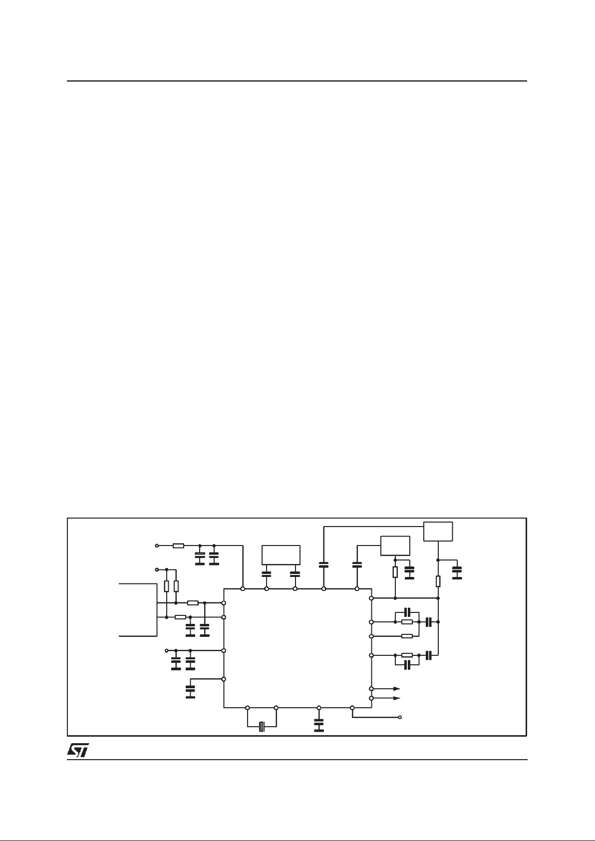
10µF 100nF
100nF
VDD2
15
VDD1
19
+10V
+5V
AM-FM
IF
IF_FM
11
IF_AM
10
10nF 10nF
TDA7427
13
12
714
INLOCK/DOUT1
SSTOP
DOUT3HFREF
8
9
VDD1
SCL
SDA
CONTROLLER
56
OSCIN OSCOUT
100nF
4
VREF
4MHz
3
6.8nF
100K
68nF
27K
6.8nF
1nF
1
2
15K
AM VCO
FM VCO
16
20
17
10nF1nF
U
tun
AM_INFM_IN
LPOUT
LP_FM
LP_HC
LP_AM
D95AU379B
10nF
10µF
3.9K 100nF
820Ω
3.3nF
FM:50KHz
AM:1KHz
Figure 6. Applicationwith two loop filters
TDA7427A
11/21

dress being transmitted.
After this comparison, the TDA7427A will generate an ”acknowledge” on the SDA line and will
perform either a read or write operation according
to the stateof R/W bit.
Write Operation
Following a START condition the master sends a
slave address word with the R/W bit set to ”0”.
The TDA7427A will ”acknowledge” after this first
transmission and wait for a second word (the
word addressfield).
This 8 bit address field provides an access to any
of the 8 internal addresses. Upon receipt of the
word address the TDA7427A slave device will respond with an ”acknowledge”. At this time, all the
following words transmitted to the TDA7427A will
be considered as Data. The internal address will
be automaticallyincremented.After each word receipt the TDA7427A will answer with an ”acknowledge”.
SOFTWARE SPECIFICATION
I
2
C Protocol
The interface protocol comprises:
A startcondition (s)
A chip address byte (the LSB determines
read/writetransmission)
A sub-addressbyte.
A sequenceof data (N-bytes + acknowledge)
A stopcondition (P)
CHIP ADDRESS
MSB LSB FUNCTION
110001C1
0 ADDR pin open
1 ADDR pin connected to V
DD
SUBADDRESS
MSB LSB FUNCTION
T3 T2 T1 I A3 A2 A1 A0
0000Charge pump control
0001PLLcounter 1 (LSB)
0010PLLcounter 2 (MSB)
0011PLLreference counter 1 (LSB)
0100PLLreference counter 2 (MSB)
0101PLLlockdetector control and PLL modeselect
0110IFCreference counter 1 (LSB)
0111IFCreferencecounter2(MSB)andIFCmode select
1000IFcounter control 1
1001IFcounter control 2
1010Oscillator adjust
1011Port extension
0 page mode off
1 page mode enabled
T1, T2, T3 used for testing, in application mode they have to be”0”
CHIP ADDRESS SUBADDRESS DATA 1 to DATA n
MSB LSB MSB LSB MSB LSB
S11000 CR/W
ACK T T T I A3 A2 A1 A0 ACK DATA ACK P
ACK = Acknowledge
S = Start
P = Stop
I = AutoIncrement
C = chip select
T = used for testing (in applicationmode they have to be ” 0”)
MAX CLOCK SPEED 400kbits/s
TDA7427A
12/21

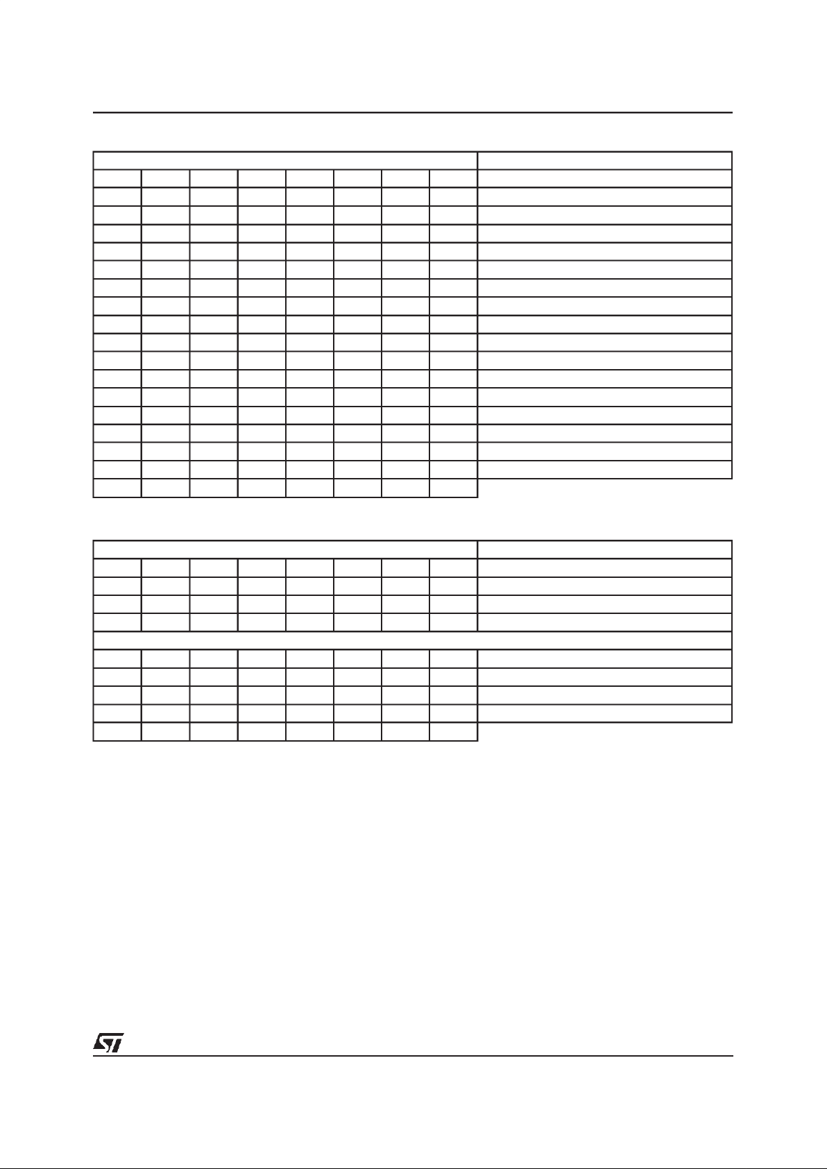
Data Byte Specification
CHARGEPUMP CONTROL
MSB LSB FUNCTION
D7 D6 D5 D4 D3 D2 D1 D0
0 0 0 0 High current = 0mA
0 0 0 1 High current = 0.5mA
0 0 1 0 High current = 1.0mA
0 0 1 1 High current = 1.5mA
0 1 0 0 High current = 2.0mA
0 1 0 1 High current = 2.5mA
0 1 1 0 High current = 3.0mA
0 1 1 1 High current = 3.5mA
1 0 0 0 High current = 4.0mA
1 0 0 1 High current = 4.5mA
1 0 1 0 High current = 5.0mA
1 0 1 1 High current = 5.5mA
1 1 0 0 High current = 6.0mA
1 1 0 1 High current = 6.5mA
1 1 1 0 High current = 7.0mA
1 1 1 1 High current = 7.5mA
0 0 Low current = 0µA
0 1 Low current = 50µA
1 0 Low current = 100µA
1 1 Low current = 150µA
0 Select low Current
1 Select high Current
1 Selectloop filter LP_FM
0 Selectloop filter LP_AM
LPIN1/2 CURRH B1 B0 A3 A2 A1 A0 Subaddress= 00H
PLL COUNTER1 (LSB)
MSB LSB FUNCTION
D7 D6 D5 D4 D3 D2 D1 D0
00000000LSB=0
00000001LSB=1
00000010LSB=2
11111100LSB=252
11111101LSB=253
11111110LSB=254
11111111LSB=255
PC7 PC6 PC5 PC4 PC3 PC2 PC1 PC0 Bit name Subaddress = 01H
TDA7427A
13/21

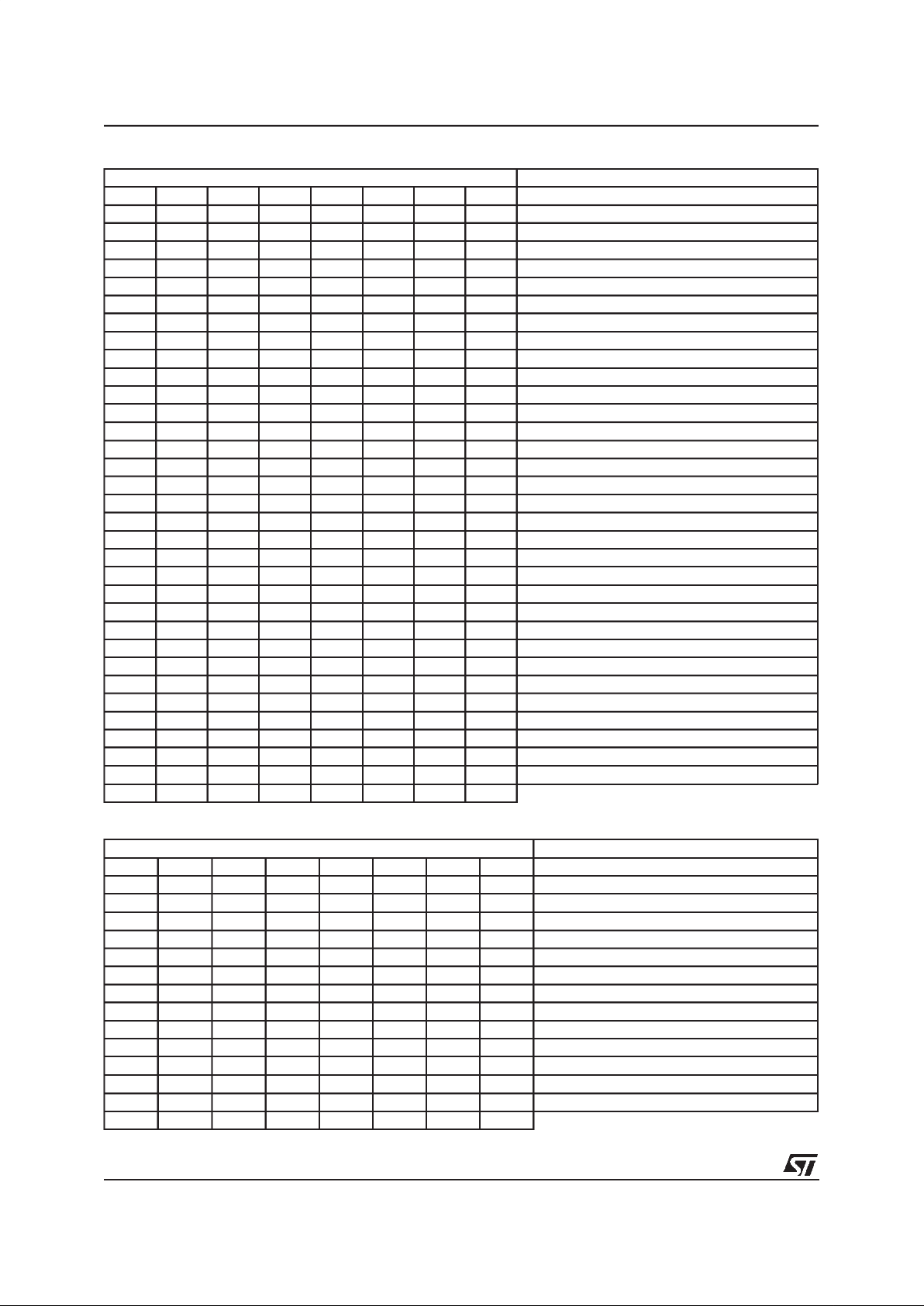
PLL COUNTER2 (MSB)
MSB LSB FUNCTION
D7 D6 D5 D4 D3 D2 D1 D0
00000000MSB=0
0 0 0 0 0 0 0 1 MSB = 256
0 0 0 0 0 0 1 0 MSB = 512
1 1 1 1 1 1 0 0 MSB = 64768
1 1 1 1 1 1 0 1 MSB = 65024
1 1 1 1 1 1 1 0 MSB = 65280
1 1 1 1 1 1 1 1 MSB = 65536
PC15 PC14 PC13 PC12 PC11 PC10 PC9 PC8 Bit name Subddress = 02H
Swallow mode: fvco/fsyn = LSB + MSB + 32
Direct mode: fvco/fsyn = LSB + MSB + 1
PLL REFERENCECOUNTER1 (LSB)
MSB LSB FUNCTION
D7 D6 D5 D4 D3 D2 D1 D0
00000000LSB=0
00000001LSB=1
00000010LSB=2
1 1 1 1 1 1 0 0 LSB = 252
1 1 1 1 1 1 0 1 LSB = 253
1 1 1 1 1 1 1 0 LSB = 254
1 1 1 1 1 1 1 1 LSB = 255
RC7 RC6 RC5 RC4 RC3 RC2 RC1 RC0 Bitname Subaddress =03H
PLL REFERENCECOUNTER2 (MSB)
MSB LSB FUNCTION
D7 D6 D5 D4 D3 D2 D1 D0
00000000MSB=0
0 0 0 0 0 0 0 1 MSB = 256
0 0 0 0 0 0 1 0 MSB = 512
1 1 1 1 1 1 0 0 MSB = 64768
1 1 1 1 1 1 0 1 MSB = 65024
1 1 1 1 1 1 1 0 MSB = 65280
1 1 1 1 1 1 1 1 MSB = 65536
RC15 RC14 RC13 RC12 RC11 RC10 RC9 RC8 Bit name Subddress = 04H
f
OSC/fREF
= LSB + MSB + 1
TDA7427A
14/21
LOCK DETECTOR& PLL MODE CONTROL
MSB LSB FUNCTION
D7 D6 D5 D4 D3 D2 D1 D0
0 0 PLL standby mode
0 1 PLL AM swallow mode
1 0 PLL AM direct mode
1 1 PLL FM mode
0 0 PD phase difference threshold 10ns
0 1 PD phase difference threshold 20ns
1 0 PD phase difference threshold 30ns
1 1 PD phase difference threshold 40ns
0 0 Not used in application mode
0 1 Activation delay = 4⋅fref
1 0 Activation delay = 6⋅fref
1 1 Activation delay = 8 ⋅ fref
0 Digital output 1 at pin ”dout1/inlock”
1 Inlock information at pin ”dout1/inlock”
0 No lock detector controlled chargepump
1 Lock detector controlled chargepump
LDENA INLOCK D3 D2 D1 D0 PM1 PM0 Bit name Subaddress = 05H
IF COUNTERREFERENCE CONTROL1 (LSB)
MSB LSB FUNCTION
D7 D6 D5 D4 D3 D2 D1 D0
00000000LSB=0
00000001LSB=1
00000010LSB=2
11111100LSB=252
11111101LSB=253
11111110LSB=254
11111111LSB=255
IRC7 IRC6 IRC5 IRC4 IRC3 IRC2 IRC1 IRC0 Bit name Subaddress = 06H
TDA7427A
15/21

IF COUNTERREFERENCE CONTROL2 (MSB)AND IF COUNTERMODE SELECT
MSB LSB FUNCTION
D7 D6 D5 D4 D3 D2 D1 D0
00000000MSB=0
0 0 0 0 0 0 0 1 MSB = 256
0 0 0 0 0 0 1 0 MSB = 512
1 1 1 1 0 1 MSB = 15616
1 1 1 1 1 0 MSB = 15872
1 1 1 1 1 1 MSB = 16128
0 0 NOT USED IN APPLICATION MODE
0 1 IF counter FM mode
1 0 IF counter AM mode
1 1 IF counter AM 10.7MHz upconversion mode
IFCM1 IFCM0 IRC13 IRC12 IRC11 IRC10 IRC9 IRC8 Bit name Subaddress= 07H
fosc/ftim = LSB + MSB + 1
IF COUNTERCONTROL 1
MSB LSB FUNCTION
D7 D6 D5 D4 D3 D2 D1 D0
0 0 0 don’tuse
0 0 1 don’tuse
011EWdeltaf=
±
6.25kHz(FM);±1kHz(AM; AM-UPC)
100EWdeltaf=±12.5kHz(FM); ±2kHz(AM;AM-UPC)
1 0 1 EWdeltaf = ±25kHz(FM); ±4kHz(AM; AM-UPC)
1 1 0 EWdeltaf = ±50Hz (FM); ±8kHz (AM;AM-UPC)
111
EW delta f =±100kHz (FM);±16kHz (AM; AMUPC)
X X X X don’t use
0 IF counter disabled / stand by
1 IF counter enabled
FENA FR3 FR2 FR1 FR0 EW2 EW1 EW0 Bit name Subaddress = 08H
TDA7427A
16/21

IF COUNTERCONTROL 2
MSB LSB FUNCTION
D7 D6 D5 D4 D3 D2 D1 D0
00000fcenter = 10.60000MHz (FM) 448KHz (AM) 10.688MHz (AM UPC)
00001fcenter = 10.60625MHz (FM) 449KHz (AM) 10.689MHz (AM UPC)
00010fcenter = 10.61250MHz (FM) 450KHz (AM) 10.690MHz (AM UPC)
00011fcenter = 10.61875MHz (FM) 451KHz (AM) 10.691MHz (AM UPC)
00100fcenter = 10.62500MHz (FM) 452KHz (AM) 10.692MHz (AM UPC)
00101fcenter = 10.63125MHz (FM) 453KHz (AM) 10.693MHz (AM UPC)
00110fcenter = 10.63750MHz (FM) 454KHz (AM) 10.694MHz (AM UPC)
00111fcenter = 10.64375MHz (FM) 455KHz (AM) 10.695MHz (AM UPC)
01000fcenter = 10.65000MHz (FM) 456KHz (AM) 10.696MHz (AM UPC)
01001fcenter = 10.65625MHz (FM) 457KHz (AM) 10.697MHz (AM UPC)
01010fcenter = 10.66250MHz (FM) 458KHz (AM) 10.698MHz (AM UPC)
01011fcenter = 10.66875MHz (FM) 459KHz (AM) 10.699MHz (AM UPC)
01100fcenter = 10.67500MHz (FM) 460KHz (AM) 10.700MHz (AM UPC)
01101fcenter = 10.68125MHz (FM) 461KHz (AM) 10.701MHz (AM UPC)
01110fcenter = 10.68750MHz (FM) 462KHz (AM) 10.702MHz (AM UPC)
01111fcenter = 10.69375MHz (FM) 463KHz (AM) 10.703MHz (AM UPC)
10000fcenter = 10.70000MHz (FM) 464KHz (AM) 10.704MHz (AM UPC)
10001fcenter = 10.70625MHz (FM) 465KHz (AM) 10.705MHz (AM UPC)
10010fcenter = 10.71250MHz (FM) 466KHz (AM) 10.706MHz (AM UPC)
10011fcenter = 10.71875MHz (FM) 467KHz (AM) 10.707MHz (AM UPC)
10100fcenter = 10.72500MHz (FM) 468KHz (AM) 10.708MHz (AM UPC)
10101fcenter = 10.73125MHz (FM) 469KHz (AM) 10.709MHz (AM UPC)
10110fcenter = 10.73750MHz (FM) 470KHz (AM) 10.710MHz (AM UPC)
10111fcenter = 10.74375MHz (FM) 471KHz (AM) 10.711MHz (AM UPC)
11000fcenter = 10.75000MHz (FM) 472KHz (AM) 10.712MHz (AM UPC)
11001fcenter = 10.75625MHz (FM) 473KHz (AM) 10.713MHz (AM UPC)
11010fcenter = 10.76250MHz (FM) 474KHz (AM) 10.714MHz (AM UPC)
11011fcenter = 10.76875MHz (FM) 475KHz (AM) 10.715MHz (AM UPC)
11100fcenter = 10.77500MHz (FM) 476KHz (AM) 10.716MHz (AM UPC)
11101fcenter = 10.78125MHz (FM) 477KHz (AM) 10.717MHz (AM UPC)
11110fcenter = 10.78750MHz (FM) 478KHz (AM) 10.718MHz (AM UPC)
11111fcenter = 10.79375MHz (FM) 479KHz (AM) 10.719MHz (AM UPC)
1 1 1 tsample = 160µs (FM mode); 1ms (AM; AM-UPC)
1 1 0 tsample = 320µs (FM mode); 2ms (AM; AM-UPC)
1 0 1 tsample = 640µs (FM mode); 4ms (AM; AM-UPC)
1 0 0 tsample = 1.280ms (FM mode); 8ms (AM; AM-UPC)
0 1 1 tsample = 2.560ms (FM mode); 16ms (AM; AM-UPC)
0 1 0 tsample = 5.120ms (FM mode); 32ms (AM; AM-UPC)
0 0 1 tsample = 10.240ms (FM mode); 64ms (AM; AM-UPC)
0 0 0 tsample = 20.480ms (FM mode); 128ms (AM; AM-UPC)
IFS2 IFS1 IFS0 CF4 CF3 CF2 CF1 CF0 bit same Subaddress = 09H
TDA7427A
17/21
OSCILLATORADJUST
MSB LSB FUNCTION
D7 D6 D5 D4 D3 D2 D1 D0
X X X 0 0 0 0 0 Cload 1,2 = 3pF
X X X 0 0 0 0 1 Cload 1,2 = 4.25pF
X X X 0 0 0 1 0 Cload 1,2 = 5.5pF
X X X 0 0 0 1 1 Cload 1,2 = 6.75pF
X X X 0 0 1 0 0 Cload 1,2 = 8pF
X X X 0 0 1 0 1 Cload 1,2 = 9.25pF
X X X 0 0 1 1 0 Cload 1,2 = 10.5pF
X X X 0 0 1 1 1 Cload 1,2 = 11.75pF
X X X 0 1 0 0 0 Cload 1,2 = 13pF
X X X 0 1 0 0 1 Cload 1,2 = 14.25pF
X X X 0 1 0 1 0 Cload 1,2 = 15.5pF
X X X 0 1 0 1 1 Cload 1,2 = 16.75pF
X X X 0 1 1 0 0 Cload 1,2 = 18pF
X X X 0 1 1 0 1 Cload 1,2 = 19.25pF
X X X 0 1 1 1 0 Cload 1,2 = 20.5pF
X X X 0 1 1 1 1 Cload 1,2 = 21.75pF
X X X 1 0 0 0 0 Cload 1,2 = 23pF
X X X 1 0 0 0 1 Cload 1,2 = 24.25pF
X X X 1 0 0 1 0 Cload 1,2 = 25.5pF
X X X 1 0 0 1 1 Cload 1,2 = 26.75pF
X X X 1 0 1 0 0 Cload 1,2 = 28pF
X X X 1 0 1 0 1 Cload 1,2 = 29.25pF
X X X 1 0 1 1 0 Cload 1,2 = 30.5pF
X X X 1 0 1 1 1 Cload 1,2 = 31.75pF
X X X 1 1 0 0 0 Cload 1,2 = 33pF
X X X 1 1 0 0 1 Cload 1,2 = 34.25pF
X X X 1 1 0 1 0 Cload 1,2 = 35.5pF
X X X 1 1 0 1 1 Cload 1,2 = 36.75pF
X X X 1 1 1 0 0 Cload 1,2 = 38pF
X X X 1 1 1 0 1 Cload 1,2 = 39.25pF
X X X 1 1 1 1 0 Cload 1,2 = 40.5pF
X X X 1 1 1 1 1 Cload 1,2 = 41.75pF
- - - OSC4 OSC3 OSC2 OSC1 OSC0 Bit name Subaddress = 0AH
PORT EXTENSIONCONTROL
MSB LSB FUNCTION
D7 D6 D5 D4 D3 D2 D1 D0
0 CMOS push-pull DOUT1 low
1 CMOS push-pull DOUT1 high
0 NPN opencollector DOUT2 inactive
1 NPN opencollector DOUT2 active
0 NPN opencollector DOUT6 inactive
1 NPN opencollector DOUT6 active
0 NPN opencollector DOUT5 inactive
1 NPN opencollector DOUT5 active
0 NPN opencollector DOUT4 inactive
1 NPN opencollector DOUT4 active
0 NPN opencollector DOUT3 inactive
1 NPN opencollector DOUT3 active
0 0 always ”0” in application mode
- - DOUT3 DOUT4 DOUT5 DOUT6 DOUT2 DOUT1 Bit name Subaddress = 0BH
TDA7427A
18/21

c
E1
k
A
be
D
E
Pin 1 identification
14
28 15
TSSO28M
Gage
Plane
0.25mm
L
0.076 mm
A1
SEATING PLANE
0.003 inch
SEATINGPLANE
A2
A1
TSSOP28 PACKAGE MECHANICAL DATA
DIM.
mm inch
MIN. TYP. MAX. MIN. TYP. MAX.
A 1.20 0.048
A1 0.05 0.15 0.002 0.006
A2 0.80 1.00 1.05 0.031 0.039 0.041
b 0.19 0.30 0.007 0.012
c 0.09 0.20 0.0035 0.008
D 9.60 9.70 9.80 0.378 0.382 0.386
E 6.40 0.252
e 0.65 0.026
E1 4.30 4.40 4.50 0.169 0.173 0.177
L 0.45 0.60 0.75 0.018 0.024 0.030
S0°(min.) 8°(max.)
TDA7427A
19/21

SO28 PACKAGEMECHANICAL DATA
DIM.
mm inch
MIN. TYP. MAX. MIN. TYP. MAX.
A 2.65 0.104
a1 0.1 0.3 0.004 0.012
b 0.35 0.49 0.014 0.019
b1 0.23 0.32 0.009 0.013
C 0.5 0.020
c1 45° (typ.)
D 17.7 18.1 0.697 0.713
E 10 10.65 0.394 0.419
e 1.27 0.050
e3 16.51 0.65
F 7.4 7.6 0.291 0.299
L 0.4 1.27 0.016 0.050
S8°(max.)
TDA7427A
20/21

Information furnished is believed to be accurate and reliable. However, STMicroelectronics assumes no responsibility for the consequences
of use of such information nor for any infringement of patents or other rights of third parties which may result from its use. No license is
granted by implication or otherwise under any patent or patent rights of STMicroelectronics. Specification mentioned in this publication are
subject to change without notice. This publication supersedes and replaces all information previously supplied. STMicroelectronics products
are not authorized for use as critical components in life support devices or systems without express written approval of STMicroelectronics.
The ST logo is a registered trademark of STMicroelectronics
1998STMicroelectronics – Printed in Italy– All Rights Reserved
STMicroelectronics GROUP OF COMPANIES
Australia - Brazil - Canada - China - France - Germany - Italy - Japan - Korea - Malaysia - Malta- Mexico - Morocco - The Netherlands -
Singapore - Spain - Sweden - Switzerland - Taiwan - Thailand - United Kingdom - U.S.A.
TDA7427A
21/21
 Loading...