

®
FRONT-END FOR AM/FM RECEIVERS
UP-CONVERSION ARCHITECTURE FOR AM
HIGH SPEED PLL WITH INLOCK DETECTOR
FOR OPTIMIZED RDS APPLICATIONS
SINGL E FR EQUE NCY REFE RENC E FO R AM/F M
AM/FM STATION DETECTOR
µP-CONTROLLED COMPENSATION OF EX-
TERNAL COMPONENTS SPREAD
ADJUSTABLE AUDI O MUTE
FULLY PROGRAMMABLE BY I2C BUS
ADVANCED BICMOS TECHN OLOGY
TDA7421
AM/FM TUNER FOR CAR RADI O
AND Hi-Fi APPLICATIONS
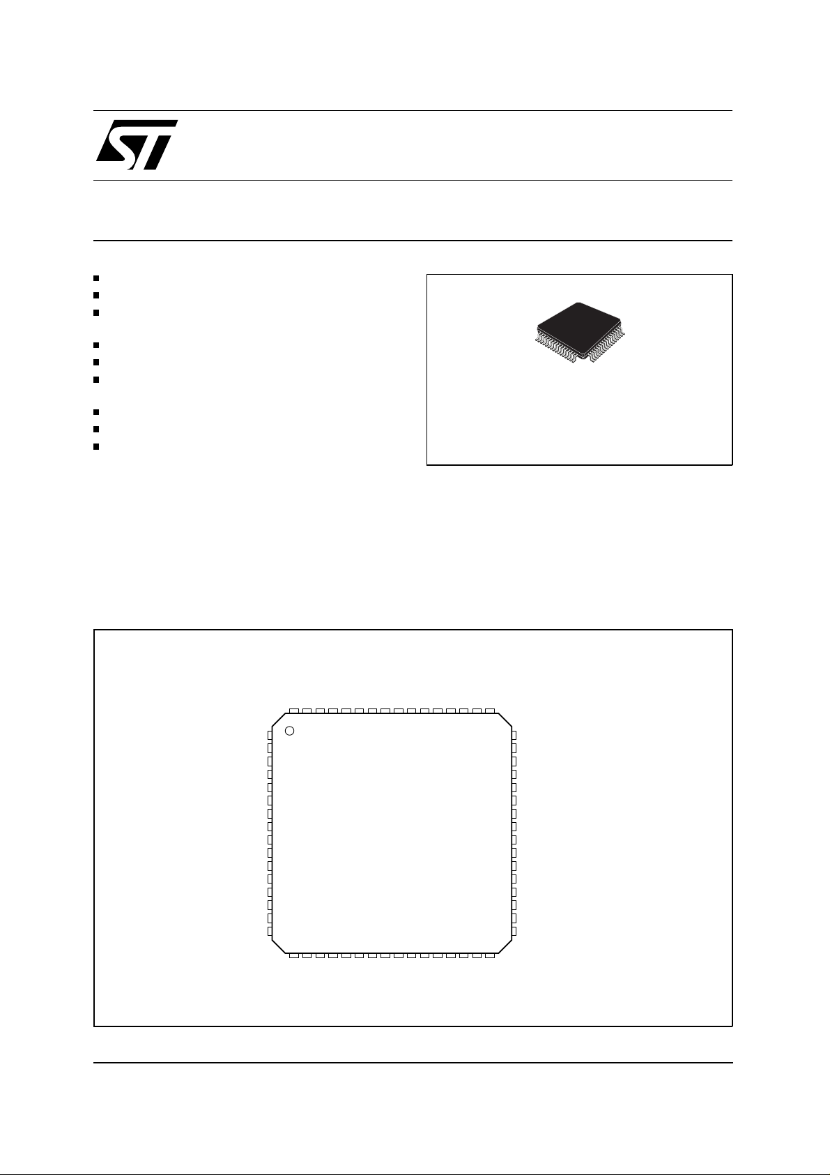
TQFP64
ORDERING NUMBER:
TDA7421
GENERAL DESCRIPTION
The TDA7421 is a high performance tuner circuit
that integrates AM/FM sections, IF counter and
PLL synthesizer on a single chip.
Use of BICMOS technology allows the im plementation of tuning functions with a minimum of external components.
Value spread of external components can be fully
PINS CONNECTION
FM IF AGC IN
AM MIX2 IN +
AM MIX2 IN-
MIX OUT -
MIX OUT +
AM AGC1 TC
AM AGC1 RF AMP
AM AGC1 PIN
60
61
62
63
AM MIX1 IN -
AM MIX1 IN +
FM MIX IN -
FM MIX IN +
FM RF AGC IN
FM AGC OUT
RF GND
VCO B
VCO E
OSC GND
XTAL D
XTAL G
OSC VCC
FM ANT ADJ
FM RF ADJ
PLL VCC
64
1
2
3
4
5
6
7
8
9
10
12
13
14
15
16
17 18 19 20 21
59 58 57 56 5455 53 52 51 50 49
22 23 24 25 26
compensated by means of on-chip electrical adjustment controlled by external µP.
The Automatic Gain Control (AGC) operates on
different sensitivities and bandwidths in order to
improve sensitivity and dynamic range. I
allows to control selected functions of the tuner
(AGC and amplifiers gain, PLL and counters operation modes).
RF VCC
AM MIX2 OUT -
AM MIX2 OUT +
FM IF AMP1 IN +
FM IF AMP1 IN -
FM IF AMP1 OUT
FM IF AMP2 IN +
FM IF AMP2 IN -
48
FM IF AMP2 OUT
47
IF1 VCC
46
FM LIM IN +
45
FM LIM IN -
44
IF1 GND
43
FM BW TC
42
FM MUTE DRIVE
FM SMETER AM SMETER
41
FM DET ADJ
40
FM SD AM SD
39
AUDIO OUT
38
FM QUAD+
37
FM QUAD-
36
IF2 VCC
35
AM IF2 IN
34
AM REF
33
AM BPF
271128 29 30 31 32
2
C bus
June 1998
LP IN1
LP OUT
LP IN2
LP IN3
PLL GND
PLL VREF
SLEEP
SDA
SCL
DIG VDD
DIG GND
IF2 GND
CLN GND
STEREO OUT
IFC SSTOP AM
D96AU546A
AM DET
AM AGC2 TC
1/38
TDA7421
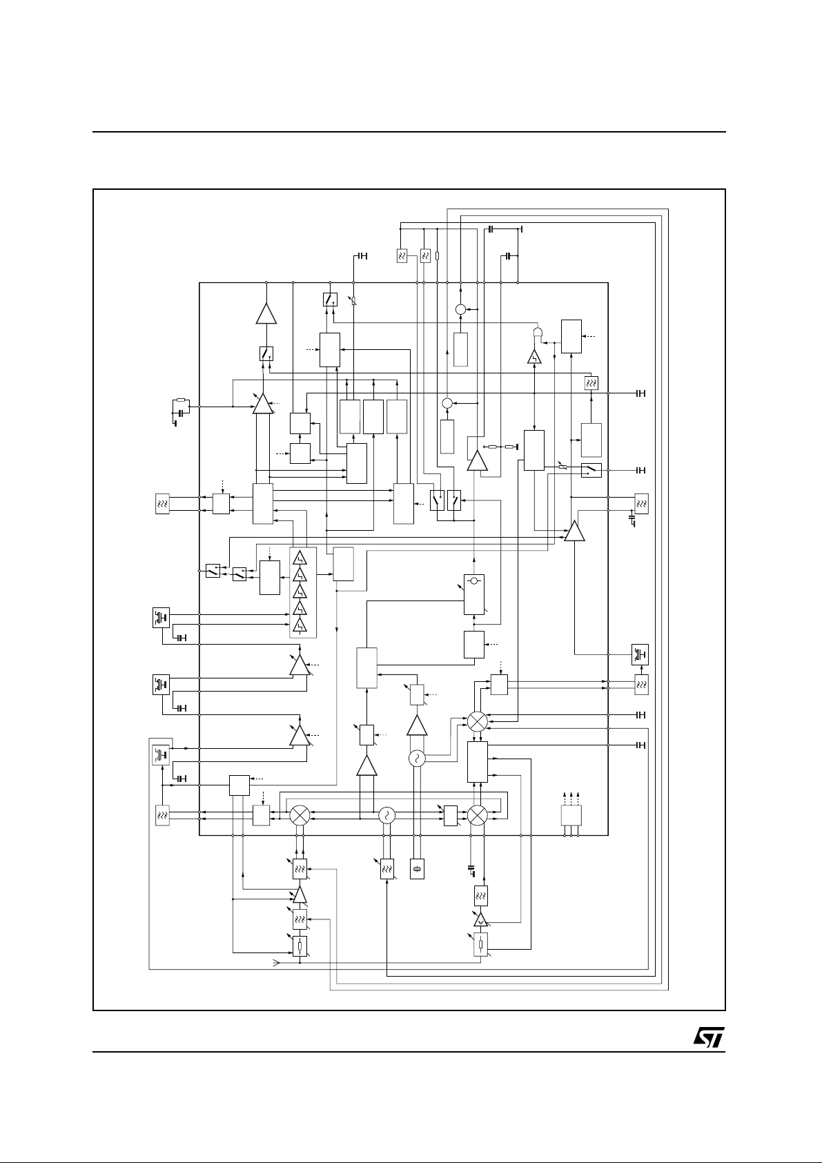
BLOCK DIAGRAM
AUDIO OUT
FM SMETER
AM SMETER
FM DET ADJ OUT
AM SD/
FM SD
BW TC
LPIN2
LPIN1
LPIN3
FM RF ADJ
FM ANT ADJ
LPOUT
PLL VCCPLL VREF
PLL GND
FM MUTE
QUAD-
QUAD+
IFC SSTOP
AM STEREO OUT
LIM IN+
LIM IN-
AMP2 OUT
FM IF
AMP2 IN+
FM IF
AMP2 INFM IF
AMP1 OUT
FM IF
AMP1 IN+
FM IF
AMP1 INFM IF
AGC IN
FM IF
MIX OUT+
MIX OUT-
FILTER
ADJ.
AM IF
AM IF
FM
AGC
FM AGC OUT
FM RF AGC IN
FM
DETECTOR
QUADRATURE
COUNT
ADJ.
FILTER
FM IF
AM
COUNTER
FM MIX
IN+
OUT
TRIPLE
SLIDER
AM
FM MIX
SMETER
LIMITER
IN-
FM SD
STOP
AM SD
STATION
MUTE
DETUNING
DETUNING
S METER
SOFT
DETECTOR
PHASE
COMPARATOR
÷
MUTE
VCOE
CH. MUTE
ADJACENT
CH. DET.
ADJACENT
OSC
10.25MHz
VCO
VCOB
XTALG
+
4 BIT DAC
AM IF
COUNTER
D96AU540A
÷
AM DET
+
4 BIT DAC
AGC
-
+
AM IF
AM
DETECTOR
AM AGC2
TC
AM
AM BPF
IFREF
-
PUMP
CHARGE
IN
DET
LOCK
ADJ.
AM RF AGC
AM MIX IN-
IN+
AM MIX
FILTER
AGC1 ANT
AM AGC1 RF AMP OUT
C
2
I
BUS
SCL
SDA
SLEEP
÷
÷
XTALD
AM IF2
OUT+
AM MIX2
OUT-
AM MIX2
IN-
AM MIX2
MIX2 IN+
AM
AGCI TC
AM
2/38

ABSOLUTE MAXIMUM RATINGS
Symbol Parameter Value Unit
T
amb
T
stg
V
CC
V
DD
Operating Temperature Range -40 to 85 °C
Storage Temperature Range -55 to 150 °C
Analog Supply Voltages (PLL, RF, IF1, IF2, OSC) 10.2 V
Digital Supply Voltage 5.5 V
THERMAL DATA
Symbol Parameter Value Unit
R
th j-amb
Thermal resistance Junction-Ambient typ. 68 °C/W
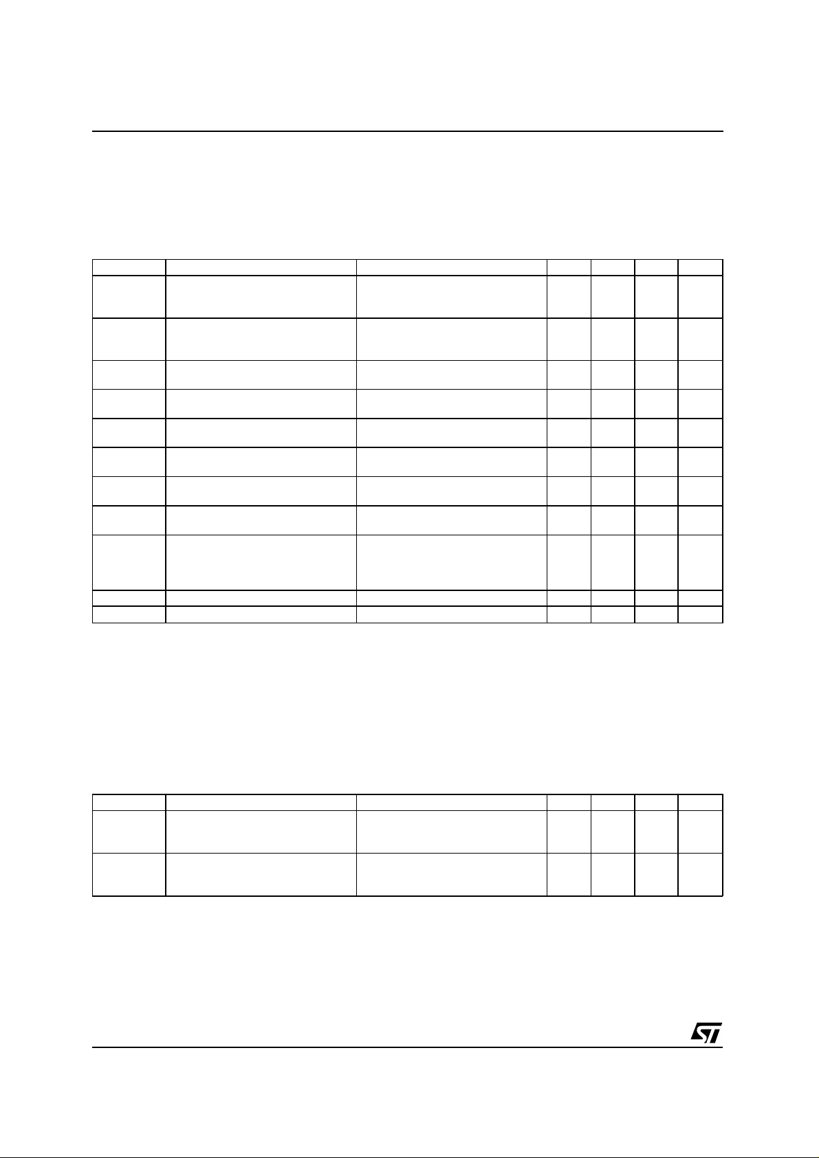
PIN DESCRIPTION
TDA7421
N. Name Function
1 AM MIX1 IN - Input "-" to the AM 1st mixer (differential input)
2 AM MIX1 IN + Input "+" to the AM 1st mixer (differential input)
3 FM MIX IN - Input "-" to the FM mixer (differential input)
4 FM MIX IN + Input "+" to the FM mixer (differential input)
5 FM RF AGC IN Input to the RF AGC circuit
6 FM AGC OUT Voltage output to the FM AGC
7 RF GND RF circuits ground
8 VCO B Local oscillator input to the transistor base (two-pin oscillator)
9 VCO E Local oscillator input to the transistor emitter (two-pin oscillator)
10 OSC GND Oscillator ground
11 XTAL D Crystal oscillator input to MOS drain (two-pin oscillator)
12 XTAL G Crystal oscillator input to MOS gate (two-pin oscillator)
13 OSC VCC Oscillator positive supply
14 FM ANT ADJ Tuning varicap voltage for antenna FM filter
15 FM RF ADJ Tuning varicap voltage for RF FM filter
16 PLL VCC PLL positive supply
17 LP OUT Op Amp output to PLL loop filters
18 LP IN1 PLL "N. 1" loop filter connection to Op Amp inverting input
19 LP IN2 PLL "N. 2" loop filter connection to Op Amp inverting input
20 LP IN3 PLL "N. 3" loop filter connection to Op Amp inverting input
21 PLL VREF Voltage reference to Op Amp noninverting input
22 PLL GND PLL ground
2
23 SLEEP I
C bus disconnect signal
24 SDA I2C bus data
2
25 SCL I
C bus clock
3/38

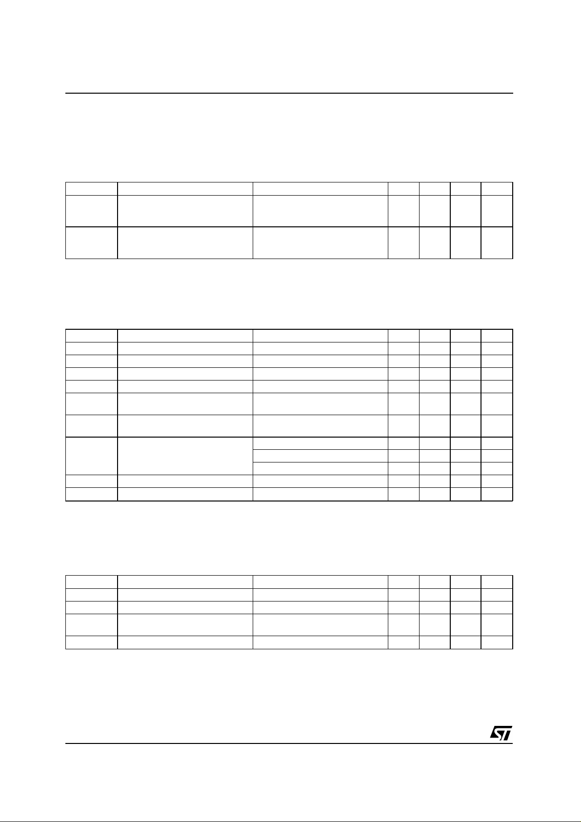
TDA7421
PIN DESCRIPTION
N. Name Function
27 DIG GND Digital circuits ground
28(*) IFC SSTOP
AM STEREO OUT
29 CLN GND "Clean" ground
30 IF2 GND IF 2nd ground
31 AM AGC2 TC AM 2nd AGC time constant
32 AM DET Connection to the capacitor of the AM diode-capacitor detector
33 AM BPF Connection to the AM IF filter
34 AM REF Reference voltage of AM IF amplifier
35 AM IF2 in Input (single ended) of AM 2nd IF amplifier
36 IF2 VCC IF 2nd positive supply
37 FM QUOD - "-" Insertion pt. of FM quadrature network (differential)
38 FM QUAD + "+" Insertion pt. of FM quadrature network (differential)
39 AUDIO OUT Audio frequency output (single ended)
40 (*) FM SD
41(*) FM SMETER
AM SMETER
FM DET ADJ
42 FM MUTE DRIVE FM mute time constant
43 FM BW TC FM detuning detector time constant
44 IF1 GND IF 1st ground
45 FM LIM IN - Input "-" of FM limiter (differential input)
46 FM LIM IN + Input "+" of FM limiter (differential input)
47 IF1 VCC IF 1st positive supply
48 FM IF AMP2 OUT Output (single ended) of the FM IF 2nd amplifier buffer
49 FM IF AMP2 IN - Input "-" of the FM IF 2nd amplifier (differential input)
50 FM IF AMP2 IN + Input "+" of the FM IF 2nd amplifier (differential input)
51 FM IF AMP1 OUT Output (single ended) of the FM IF 1st amplifier buffer
52 FM IF AMP1 IN - Input "-" of the FM IF 1st amplifier (differential input)
53 FM IF AMP1 IN + Input "+" of the FM IF 1st amplifier (differential input)
54 AM MIX2 OUT - Output "-" of the AM 2nd mixer (differential output)
55 AM MIX2 OUT + Output "+" of the AM 2nd mixer (differential output)
56 RF VCC RF stage positive supply
57 AM MIX2 IN - Input "-" to the AM 2nd mixer (differential input)
58 AM MIX2 IN + Input "+" to the AM 2nd mixer (differential input)
59 FM IF AGC IN Input FM IF AGC circuit
60 MIX OUT - Output "-" of the FM/AM 1st mixer (differential output)
61 MIX OUT + Output "+" of the FM/AM 1st mixer (differential output)
62 AM AGC1 TC AM 1st AGC time constant
63 AM AGC1 RF AMP Voltage output of the AM 1st AGC, to the transistor of the RF AF amplifier
64 AM AGC1 PIN Current output of the AM 1st AGC, to the PIN diodes antenna AM attenuator
(*) Pin function is user-defined by software.
AM SD
(continued)
Search stop signal or
Output (single ended) of AM IF amplifier
FM Station detector output or
AM Station detector output
FM S-meter output or
AM S-meter output or
FM detuning adjustment
4/38
TDA7421
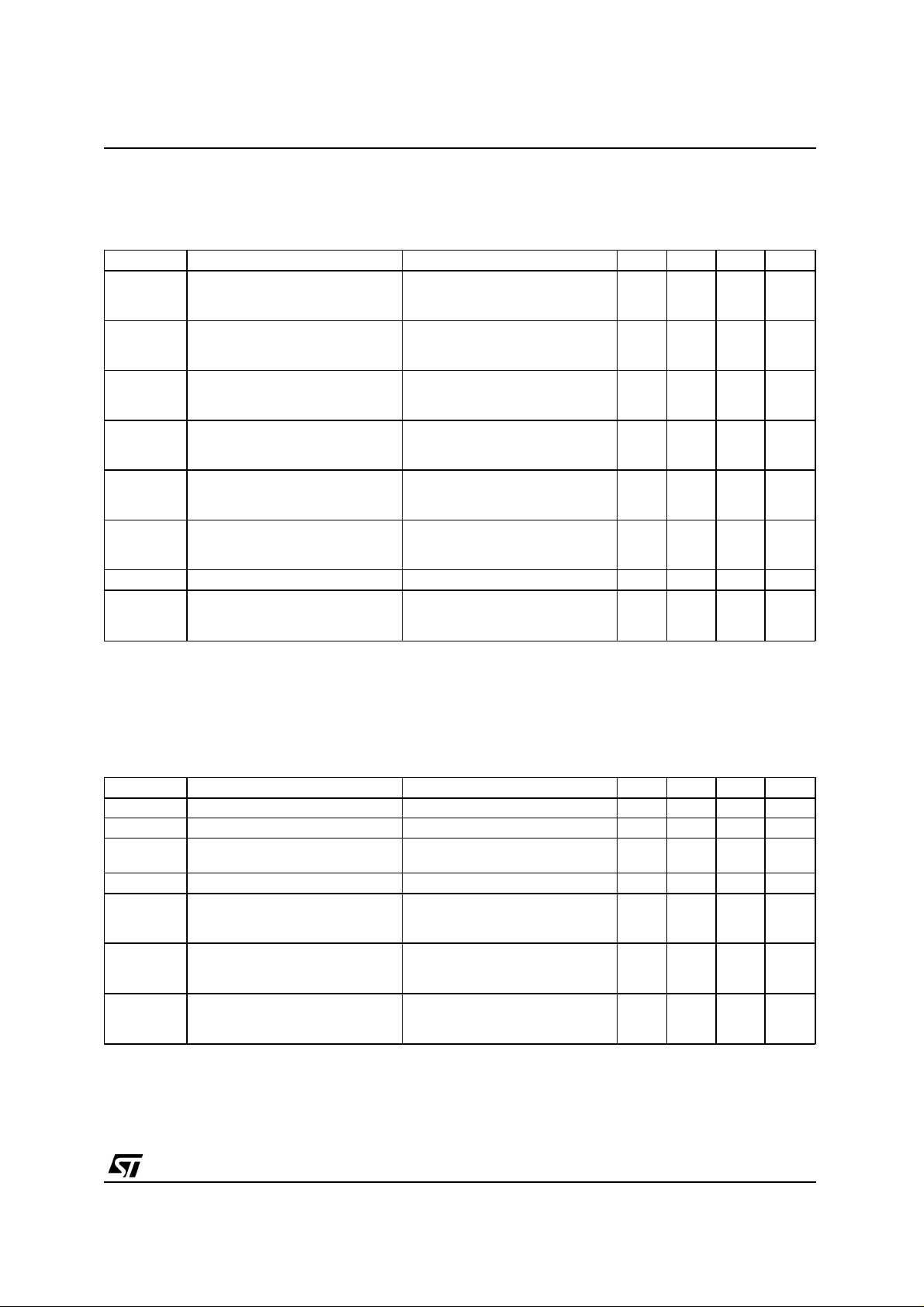
ELECTRICAL CHARACTERISTICS
DC PARAMETERS
amb
(T
= 25°C; Vcc = 8.5V, Vdd = 5V unless otherwise specified)
Symbol Parameter Test Condition Min. Typ. Max. Unit
DIG V
DIG I
Digital Supply Voltage 4.75 5.25 V
dd
Digital Supply Current AM MODE 4.0 4.6 5.2 mA
dd
FM MODE 3.5 4.0 4.5 mA
PLL V
PLL I
PLL Supply Voltage 7.5 10 V
CC
PLL Supply Current AM MODE 1.2 1.6 2.0 mA
CC
FM MODE 2.5 3.0 3.5 mA
RF V
RF I
RFSupply Voltage 7.5 10 V
CC
RF Supply Current AM MODE 15.0 17.5 20.0 mA
CC
FM MODE 10.0 13.0 16.0 mA
IF1 V
IF1 I
IF1 Supply Voltage 7.5 10 V
CC
IF1 Supply Current AM MODE 2.2 2.7 3.2 mA
CC
FM MODE 16.0 19.5 23.0 mA
IF2 V
IF2 I
IF2 Supply Voltage 7.5 10 V
CC
IF2 Supply Current AM MODE 8.5 10.5 12.5 mA
CC
FM MODE 27.0 32.0 37.0 mA
OSC V
OSC I
Oscillator Supply Voltage 7.5 10 V
CC
Oscillator Supply Current AM MODE 14.5 17.0 19.5 mA
CC
FM MODE 11.0 14.0 17.0 mA
TOTAL I
Total Supply Current AM MODE 45.0 50.0 55.0 mA
CC
FM MODE 73.0 81.0 89.0 mA
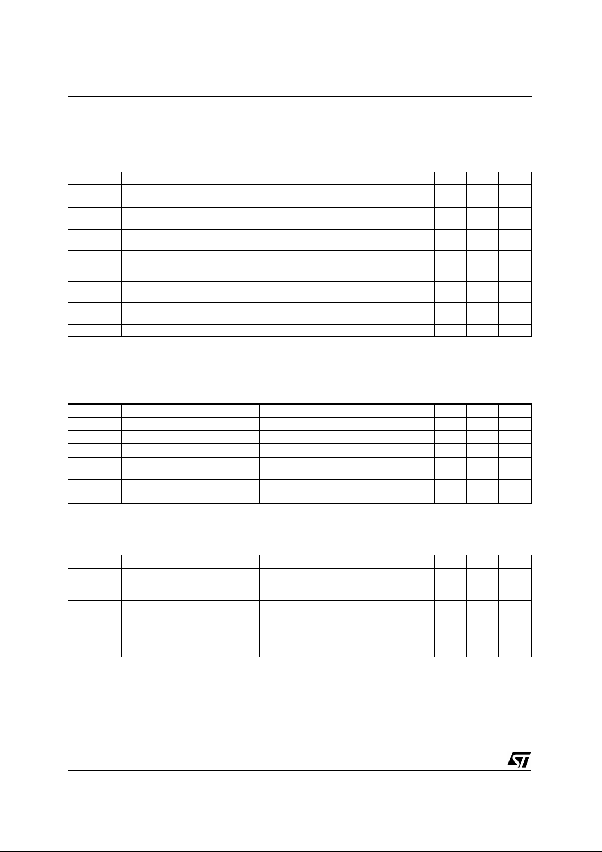
AC PARAMETERS
osc
Ref: FM Test Circuit measure V
with high impedance FET probe
Voltage Controlled Oscillator (VCO)
Symbol Parameter Test Condition Min. Typ. Max. Uni
f
VCOmin
f
VCOmax
V
OSC
Minimum VCO Frequency V
Maximum VCO Frequency V
Oscillator Amplitude fosc = 108.8MHz, Europe/USA
= 0, Europe/USA
turn
Japan
= VCC, Europe/USA
turn
Japan
f
= 72.3MHz, Japan
OSC
123.2
79.2
80.95598.2
65.4
128
90
106 dBu
Reference Oscillator
XTAL
Ref: AM Test Circuit measure V
Symbol Parameter Test Condition Min. Typ. Max. Uni
f
V
XTAL
XTAL
Reference Frequency 10.25 MHz
Oscillator Amplitude 108 dBu
with high impedance FET probe
MHz
MHz
MHz
MHz
5/38

TDA7421
ELECTRICAL CHARACTERISTICS
(continued)
FM Section Global Performances
Refer to Evaluation Circuit and enclosed curves (S+N/N, THD)
- RF Input: f
= 98.1MHz, 75KHz dev., 1KHz mod.,60dBu
c
- Audio Output: BPF 20Hz - 20KHz
Symbol Parameter Test Condition Min. Typ. Max. Uni
S+N/N Signal to Noise Ratio 68 dB
THD Total Harmonic Distortion deviation = 40KHz 0.3 %
V
O AF
US Usable Sensitivity antenna level at which
Audio Output Level 350 400 450 mV
4dBu
S+N/N=30dB
AGC
range
Range AGC FM 65 dB
FM Front-e nd E le ctr ic al Ad jus tm en t s
Ref: FM Test Circuit measure V
ANTADJ
Symbol Parameter Test Condition Min. Typ. Max. Uni
ANTADJ
MAX OFF
ANTADJ
STEP OFF
RFADJ
MAX OFF
RFADJ
STEP OFF
Maximum FM Antenna Filter
Adjustment Voltage Offset
FM Antenna Filter Adjustment
Voltage Offset Step
Maximum FM RF Filter
Adjustment Voltage Offset
FM RF Filter Adjustment Voltage
Offset Step
and V
RFADJ
referred to V
V
PLLOUT
1111
V
PLLOUT
1001
V
PLLOUT
1111
V
PLLOUT
1001
PLLOUT
= 2.5V, ANA3-0 set to
= 2.5V, ANA3-0 set to
= 2.5V, RFA3-0 set to
= 2.5V, RFA3-0 set to
21 25 27 %
2.8 3.6 4.4 %
21 25 27 %
2.8 3.6 4.4 %
RMS
FM Mixer
Ref: FM Test Circuit, measure input at V
MIXFMIN
, output at V
Symbol Parameter Test Condition Min. Typ. Max. Unit
Z
IN,MIX
Single-ended input impedance
f = 100MHz 12 Ω
(pin 3, pin4)
G
IP3
CP1
MIX
MIX
Conversion Gain fIN = 98.1MHz 21.8 dB
3rd order intermodulation
distortion intercept point
1dB compression point fIN = 98.1MHz 90 dBu
MIX
fd = 98.1MHz; fu1 = 98.2MHz;
f
= 98.3MHz;
u2
MIXOUT
104 dBu
FM AGC
Ref: FM Test Circuit, measure input at V
FMRFAGCIN
, and V
Symbol Parameter Test Condition Min. Typ. Max. Unit
V
RFAGCSTART
R
INRFAGC
V
IFAGCSTART
Open Loop Rf Agc Starting Point f
RFAGCIN
V
FMRFAGCIN
V
FMAGCOUT
Input Resistance 20 KΩ
Open Loop If Agc Starting Point f
IFAGCIN
V
FMIFAGCIN
V
FMAGCOUT
FAGC2-0 set to 111
R
INIFAGC
R
OUTFMAGC
Input Resistance 20 KΩ
Output Resistance 10 KΩ
FMIFAGCIN
, output at V
= 98.1MHz Value of
, at which
= 4V
= 10.7MHz Value of
, at which
= 4V
FMAGCOUT
74 80 86 dBu
71 77 83 dBu
6/38
TDA742 1
ELECTRICAL CHARACTERISTICS
FM IF Amplifier 1
Ref: FM Test Circuit, measure input at V
(continued)
FMAMP1IN
, output at V
FMAMP1OUT
Symbol Parameter Test Condition Min. Typ. Max. Unit
R
IN,AMP1
R
OUT,AMP1
G
TYP,AMP1
Input Resistance f = 10.7MHz 330 Ω
Output Resistance f = 10.7MHz 330 Ω
Typical Gain fIN = 10.7MHz, FBH3-0 set to
16.5 17.5 18.5 dB
0100
G
MIN,AMP1
Minimum Gain fIN = 10.7MHz, FBH3-0 set to
14.5 15.5 16.5 dB
0001
G
MAX,AMP1
Maximum Gain fIN = 10.7MHz, FBH3-0 set to
18.5 19.5 20.5 dB
0000
IP3
CP1
AMP1
AMP1
3rd Order Intermodulation
Distortion Intercept Point
1dB Compression Point fIN = 10.7MHz; FBH3-0 set to
fd = 10.7MHz; fu1= 10.8MHz; fu2=
10.9MHz, FBH3-0 set to 0100
109 dBu
96 dBu
0100
FM IF Amplifier 2
Ref: FM Test Circuit, measure input at V
FMAMP2IN
, output at V
Symbol Parameter Test Condition Min. Typ. Max. Unit
R
IN,AMP2
R
OUT,AMP2
G
TYP,AMP2
G
MIN,AMP2
G
MAX,AMP2
IP3
CP1
AMP2
AMP2
Input Resistance f = 10.7MHz 330 Ω
Output Resistance f = 10.7MHz 330 Ω
Typical Gain fIN = 10.7MHz, FBL3-0 set to 0100 5 6 7 dB
Minimum Gain fIN = 10.7MHz, FBL3-0 set to 0001 3 4 5 dB
Maximum Gain fIN = 10.7MHz, FBL3-0 set to 0000 7 8 9 dB
3rd Order Intermodulation
Distortion Intercept Point
fd = 10.7MHz; fu1= 10.8MHz; fu2=
10.9MHz, FBL3-0 set to 0100
1dB Compression Point fIN = 10.7MHz; FBL3-0 set to 0100 110 dBu
FMAMP2OUT
122 dBu
FM Limiter, Field Strengh Meter and Demodulator
Ref: FM Test circuit, measure:
- Input at V
FMLIMIN
- filtered FS Meter output at V
- shifted FS Meter output at V
- demodulator adjustment output at V
Symbol Parameter Test Condition Min. Typ. Max. Unit
R
IN,LIM
G
LIM
LS Limiting Sensitivity 23 dBu
SM1 Smeter 1 at V
SM2 Smeter 2 at V
SM3 Smeter 3 at V
SM
MINSHIFT
SM
MAXSHIFT
G
DEM
G
DEMADJ
NOTE1: Refer to Global application circuit; input at first Ceramic Filter in, FBH3-0 set to 0001, FBL3-0 set to 0001
, fIN = 10.7MHz
SM,FILT
SM,SHIFT
Limiter Input Resistance 330 Ω
Limiter Gain 90 dB
SM,FILT
SM,FILT
SM,FILT
Smeter Minimum Shift Voltage at
V
SM,SHIFT
referred to V
Smeter Maximum Shift Voltage
at V
SM,SHIFT
referred to V
Demodulator Conversion Gain V
Demodulator Adjustment
Conversion Gain
(FMADJ set to 0)
SM,SHIFT
SM,FILT
SM,FILT
(FMADJ set to 1)
V
V
V
V
00000
V
11111
V
V
= 42dBu 0.1
FMLIMIN
= 77dBu 2.4
FMLIMIN
= 102dBu 4.0
FMLIMIN
= 70dBu, FSL4-0 set to
FMLIMIN
= 70dBu, FSL4-0 set to
FMLIMIN
> LS 2 mV
FMLIMIN
> LS, measured at
FMLIMIN
, FMADJ set to 1
SMSHIFT
(1)
0.25 0.5
(1)
2.75 3.1
(1)
4.35 4.7
0.25 0.3 0.35 V
1.55 1.8 2.05 V
14 mV
(1)
(1)
(1)
V
V
V
RMS
KHz
RMS
KHz
7/38
/
/
TDA7421
ELECTRICAL CHARACTERISTICS
(continued)
FM Audio Amplifier
Ref: FM Test circuit, measure:
- Input at V
FMLIMIN
- audio output at V
- muting voltage at V
Symbol Parameter Test Condition Min. Typ. Max. Unit
V
MUTE
V
PLAY
G
AMP,PLAY
G
AMP,MUTE MAX
G
AMP,MUTE MIN
V
AF
THD AFTotal Harmonic distortion f
S+N/N AF Signal to Noise Ratio f
AMR Amplitude Modulation Rejection AM modulation deph 30%, f
AUDIO
curr
MUTE R
NOTE1: Refer to Global application circuit; input at first Ceramic Filter in, FBH3-0 set to 0001, FBL3-0 set to 0001
out
, = 95dBu, fIN = 10.7MHz
AUDIO
, BPF 20Hz to 20KHz
MUTE , DRIVE
Mute Voltage V
MUTE,DRIVE
29dB, FMHIGH set to 0, AUM2-0
set to 111
Play Voltage V
MUTE,DRIVE
1dB, FMHIGH set to 0, AUM2-0
set to 111
Audio Amplifier Gain in Play
V
MUTE,DRIVE
Conditions
Audio Amplifier Highest Gain in
Mute Condition
Audio Amplifier Lowest Gain in
Mute Condition
AF Output Level f
V
MUTE,DRIVE
set to 1, AUM2-0 set to 001
V
MUTE,DRIVE
set to 0, AUM2-0 set to 111
DEV
V
MUTE,DRIVE
DEV
V
MUTE,DRIVE
DEV
V
MUTE,DRIVE
1KHz, with respect to FM
modulated signal with f
40KHz, V
Audio Out Current Capability 5 mA
Mute Drive Output Resistance 1 KΩ
for which ∆VAF = -
for which ∆VAF = -
< V
> V
> V
= 75KHz, F
< V
= 75KHz, F
< V
= 75KHz, F
< V
MUTE,DRIVE
PLAY
MUTE
MUTE
MOD
MUTE
MOD
MUTE
MOD
MUTE
, FMHIGH
, FMHIGH
= 1KHz,
= 1KHz,
= 1KHz,
=
DEV
< V
MUTE
MOD
2V
0.3 V
9dB
6.5 dB
-21 dB
350
(1)
400 450
(1)
0.5 %
(1)
68
=
60
75 %
(1)
67 dB
mV
RMS
FM QUALITY DETECTORS
Field Strength Detector
Ref: FM Test Circuit, measure:
- Input at V
FMLIMIN
- output at V
Symbol Parameter Test Condition Min. Typ. Max. Unit
FSD
MIN
FSD
MAX
8/38
, fIN = 10.7MHz, CW
MUTE,DRIVE
Field Strenght Detector Minimum
Threshold
Field Strenght Detector Maximum V
V
FMLIMIN
V
MUTE,DRIVE
to 0000
FMLIMIN
V
MUTE,DRIVE
to 1111
level at which
= V
, FSM3-0 set
MUTE
level at which
= V
, FSM3-0 set
MUTE
40 dBu
60 dBu

TDA7421
ELECTRICAL CHARACTERISTICS
(continued)
Detuning Detector
Ref: FM Test Circuit, measure:
- Inputs at V
FMLIMIN
- output at V
Symbol Parameter Test Condition Min. Typ. Max. Unit
DD
START
DD
SLOPE,MIN
DD
SLOPE,MAX
DD
TRC
, CW
MUTE,DRIVE
Detuning Detector Starting Point frequency shift from 10.7MHz at
Detuning Detector Minimum
Muting Slope
Detuning Detector Maximum
Muting Slope
Detuning Detector Time Constant
Ratio
which V
MUTE,DRIVE
= V
PLAY
frequency shift from 10.7MHz +
DD
V
at which V
START,
BWM2-0 set to 100,
MUTE,
MUTE,DRIVE
FMRECSEEK set to 0
frequency shift from 10.7MHz +
DD
V
at which V
START,
BWM2-0 set to 001,
MUTE,
MUTE,DRIVE
FMRECSEEK set to 0
ratio of "reception" mode
integration time constant inside the
Detuning Detector with respect to
"seek" mode
±23 KHz
22.5 30 37.5 KHz
=
7.5 10 12.5 KHz
=
34/6 s/s
Adjacent Channel Detector
Ref: FM Test Circuit, measure:
- Inputs at V
- output at V
FMLIMIN
: desired 10.7MHz, 95dBu CW; undesired 10.8MHz CW
MUTE,DRIVE
- BWM2-0 set to 001
Symbol Parameter Test Condition Min. Typ. Max. Unit
ACD
MAX
Adjacent Channel Quality Detector
Maximum Sensitivity Threshold
amplitude of undesired signal at
which V
MUTE,DRIVE
= V
MUTE
,
91 dBu
HDM4-0 set to 11111
ACD
Adjacent Channel Quality Detector
MIN
Minimum Sensitivity Threshold
amplitude of undesired signal at
which V
MUTE,DRIVE
= V
MUTE
,
94.8 dBu
HDM4-0 set to 00000
Field Strength Station Detector
Ref: FM Test Circuit, measure:
- Inputs at V
- output at V
FMLIMIN
: desired 10.7MHz, CW
FMSD
- FMRECSEEK set to 1
Symbol Parameter Test Condition Min. Typ. Max. Unit
FSSD
FSSD
Field Strength Station Detector
MIN
Minimum Threshold
Field Strength Station Detector
MAX
Maximum Threshold
V
V
V
V
level at which
FMLIMIN
= 2.5, FSM4-0 set to 00000
FMSD
level at which
FMLIMIN
= 2.5, FSM4-0 set to 11111
FMSD
24 dBu
76 dBu
Detuning Sta tion Detector
Ref: FM Test Circuit, measure:
- Input at V
- output at V
FMLIMIN
FMSD
, CW;
- FMRECSEEK set to 1
Symbol Parameter Test Condition Min. Typ. Max. Unit
DSD Detuning Station Detector
Threshold
frequency shift from 10.7MHz at
which V
FMSD
= 2.5V
23 KHz
9/38
TDA7421
ELECTRICAL CHARACTERISTICS
(continued)
Adjacent Channel Station Detector
Ref: FM Test Circuit, measure:
- Input at V
- output at V
FMLIMIN
: desired 10.7MHz, 95dBu CW; undesired 10.8MHz CW
FMSD
- FMRECSEEK set to 1
Symbol Parameter Test Condition Min. Typ. Max. Unit
ACSD
Adjacent Channel Detector
MAX
Maximum Sensitivity Threshold
amplitude of undesired signal at
which V
= 2.5V, HDM4-0 set
FMSD
92.5 dBu
to 11111
ACD
Adjacent Channel Detector
MIN
Minimum Sensitivity Threshold
amplitude of undesired signal at
which V
= 2.5V, HDM4-0 set
FMSD
94.9 dBu
to 00000
AM Section Global Performances
Refer to E v aluatio n Circui t a nd enclosed curves ( S +N /N, TH D)
- RF Input: f
c
= 1MHz, f
mod
= 1KHz, m = 0.3;
- Audio Output: BPF 20Hz - 20KHz
Symbol Parameter Test Condition Min. Typ. Max. Unit
V
IN MIN
V
∆V
IN US
Maximum Sensitivity V
Usable Sensitivity S+N/N = 20dB 31 dBu
AGC Range V
is
S+N/N Signal to Noise Ratio V
α
IMAG
α
Tw
Image Rejection f1 = 1.9MHz
Tweet V
THD Total Harmonic Distortion V
V
V
AF
AMST
Audio Output Level V
AM IF2 Output level V
= 74dBu; ∆VAF = - 20dB 20 dBu
INRF
= 74dBu; ∆VAF = -10dB 50 dB
INRF
= 74dBu 46.0 53.0 dB
INRF
f
= 22.4MHz
2
= 74dBu; f1 = 900KHz;
INRF
1.2 dB
f2 = 1350KHz
= 74dBu; m = 0.3 0.45 1.0 %
INRF
V
= 74dBu; m = 0.8 1.73 %
INRF
V
= 120dBu; m = 0.3 0.33 %
INRF
= 74dBu 137 167 197 mV
INRF
= 74dBu 106 dBu
INRF
dB
RMS
AM Mixer 1
Ref: AM Test Circuit, measure input at V
MIX2AMIN
, output at V
Symbol Parameter Test Condition Min. Typ. Max. Unit
R
INMIX1
G
IP3
CP1
MIX1
MIX1
MIX1
Input Resistance 1.2 KΩ
Conversion Gain fIN = 1MHz 7.5 8.5 9.5 dB
3rd Order Intermodulation
Distortion Intercept Point
fd = 1MHz; fu1 = 1.1MHz;
f
= 1.2MHz;
u2
1dB Compression Point fIN = 1MHz 98.7 dBu
10/38
MIXOUT
115 dBu
TDA7421
ELECTRICAL CHARACTERISTICS
(continued)
AM Wide & Narrow AGC
Ref: AM Test Circuit, input at V
MIX1AMIN
, and V
Symbol Parameter Test Condition Min. Typ. Max. Unit
V
WAGCTYP
Open Loop WIDE AGC Typical
Starting Point
V
WAGCMIN
Open Loop WIDE AGC Minimum
Starting Point
V
WAGCMAX
Open Loop WIDE AGC Maximum
Starting Point
V
NAGCTYP
Open Loop NARROW AGC
Typical Starting Point
V
NAGCMIN
Open Loop NARROW AGC
Minimum Starting Point
V
NAGCMAX
Open Loop NARROW AGC
Maximum Starting Point
R
OUTAMAGC1
I
AMAGC1PIN
Output Resistance 23.3 KΩ
Maximum Pin-diode Current f
MIX2AMIN,
f
WAGCIN
1000; V
V
AMAGC1AMP
f
WAGCIN
0000; V
V
AMAGC1AMP
f
WAGCIN
1111; V
V
AMAGC1AMP
f
NAGCIN
to 1000; V
V
AMAGC1AMP
f
NAGCIN
to 0000; V
V
AMAGC1AMP
f
NAGCIN
to 1111; V
V
AMAGC1AMP
WAGCIN
V
MIX1AMIN
output at V
= 1MHz, AAG3-0 set to
= 1MHz, AAG3-0 set to
= 1MHz, AAG3-0 set to
= 10.7MHz, AAG3-0 set
= 10.7MHz, AAG3-0 set
= 10.7MHz, AAG3-0 set
= 1MHz;
at which
MIX1AMIN
= 2.5V
at which
MIX1AMIN
= 2.5V
at which
MIX1AMIN
= 2.5V
MIX2AMIN
= 2.5V
MIX2AMIN
= 2.5V
MIX2AMIN
= 2.5V
= 90dBu; AAG3-0 set to
0000
at which
at which
at which
AMAGC1AMP
AMAGC1PIN
, andV
91.3 dBu
80.6 dBu
95.6 dBu
93.2 dBu
82.8 dBu
97.4 dBu
1.4 mA
AM Mixer 2
Ref: AM Test Circuit, m easure input at V
MIX2AMIN
, output at V
MIX2OUT
, (switches must be in position 2 for
AGC measurements).
Symbol Parameter Test Condition Min. Typ. Max. Unit
R
G
IP3
CP1
AGC
AGC
AGC
INMIX2
MIX2
MIX2
MIX2
MIXCP
MIXSP
MIXR
Input Resistance 5 KΩ
Maximum conversion Gain fIN = 10.7MHz 19.6 dB
3rd Order Intermodulation
Distortion Intercept Point
fd = 10.7MHz; fu1 = 10.8MHz;
f
= 10.9MHz;
u2
122 dBu
1dB Compression Point fIN = 10.7MHz 90.7 dBu
Central Point of AGC2 Intevention
on Mixer 2
AGC2 Starting Point on Mixer 2 fIN = 10.7MHz; Value of V
fIN = 10.7MHz;
V
Value of V
for which V
MIX2AMIN
= 52dBu;
MIX2OUT
MIX2OUT
is AGC
MIX2AMIN
-
MIXCP
61.2 dBu
40 dBu
3dB
AGC2 Range on Mixer 2 fIN = 10.7MHz; Range of
V
AGC
MIX2AMIN
MIXCP
for which V
±3dB
MIX2OUT
is
24 dB
11/38
TDA7421
ELECTRICAL CHARACTERISTICS
(continued)
AM IF2 Amplifier
Ref: AM Test Circuit, measure input at V
IN
= 450KHz.
f
IP2AMPIN
, output at V
Symbol Parameter Test Condition Min. Typ. Max. Unit
R
IN,IF2AMP
G
IF2AMP
AGC
AGC
AGC
AGC
AMPCP
AMPSP
AMPR
Input Resistance 2 KΩ
Maximum Gain V
Central Point of AGC2 Intevention
on IF2 Amp
V
V
AGC2 Starting Point on IF2 Amp Value of V
V
= 10dBu 51 dB
IF2AMPIN
= 72dBu; Value of
IF2AMPIN
IF2AMPOUT
IF2AMPOUT
IF2AMPIN
AGC2 Range on IF2 Amp fIN = 10.7MHz; Range of
V
AGC
AGC2 Time Constant Ratio Ratio of AGC2 "reception" Time
TCR
MIX2AMIN
MIXCP
= for which V
±3dB
Constant and "seek" Time Constant
IF
AMST
AM IF2 Output Level at pin 28 V
IF2AMPIN
= 72dBu;
AMSTEREO set to 1
IF
AMSTcurr
Current Capability of pin 28 AMSTEREO set to 1 150 µA
is AGC
IP2AMPOUT
for which
- 3dB
AMPCP
MIX2OUT
, (switches must be in position 1),
115 dBu
63 dBu
36 dB
is
150/5 s/s
104 106 108 dBu
AM Field Strength Meter and Field Strength Station Detector
Ref: AM Test Circuit, measure at V
IN
= 10.7KHz.
- f
MIX2AMIN
, outputs at V
AMSMETER
and at V
AMSD
(switches in position 2),
- AMSEE K set to 1
Symbol Parameter Test Condition Min. Typ. Max Unit
AMSM1 AM Smeter 1 at V
AMSM2 AM Smeter 2 at V
AMSM3 AM Smeter 3 at V
AMSD
Station Detector Minimum
MIN
Threshold
AMSD
Station Detector Maximum
MAX
Threshold
AMSMETER
AMSMETER
AMSMETER
V
V
V
V
ASS3-0 set to 0000
V
ASS3-0 set to 1111
= 35dBu 2.2 2.89 3.6 V
MIX2AMIN
= 65dBu 2.5 3.26 4.0 V
MIX2AMIN
= 95dBu 3.0 3.73 4.5 V
MIX2AMIN
MIX2AMIN
MIX2AMIN
at which V
at which V
AMSD
AMSD
= 2.5V,
= 2.5V,
44 dBu
64 dBu
IF Counter Output
Ref: AM & FM Test Circuit, measure at pin 28
Symbol Parameter Test Condition Min. Typ. Max Unit
IFC
12/38
IFC
IFC
FM
AM
current
FM IFC Sensitivity V
FMRECSEEK set to 1, EW2-0 set
to 101, IFS2-0 set to 010
AM IFC Sensitivity V
AMSEEK set to 1, EW2-0 set to
011, IF2-0 set to 100, AMFM
STBY1-0 set to 10
IFC Current Capability 150 µA
at which Vpin 28 = 2.5V,
FMLIMIN
at which Vpin 28 = 2.5V,
IF2AMPIN
34 dBu
29 dBu

TDA742 1
ELECTRICAL CHARACTERISTICS
(continued)
Loop Filte r In put Output
(LP_IN1, LP_IN2, LP_IN3, LP_OUT)
Symbol Parameter Test Condition Min. Typ. Max. Unit
-I
V
V
I
OUT
I
OUT
IN
I
IN
OL
OH
Input Leakage Current VIN = GND; PD
Input Leakage Current VIN = VDD; PD
Output Voltage Low IIN = -0.2mA; VCC = 8.5V 0.5 V
Output Voltage High I
Output Current Sink V
= 0.2mA; V
OUT
= 8.5V; 10 mA
PLL
Output Current Source Vout = 0.5 to 8V 10 mA
= Tristate 1) -2 0 2 µA
out
= Tristate -2 0 2 µA
out
= 8.5V 8 V
CC
I2C Bus Interface
Symbol Parameter Test Condition Min. Typ. Max Unit
f
SCL
t
AA
t
buf
t
HD-STA
t
LOW
t
HIGH
SCL Clock Frequency 100 500 KHz
SCL Low to SDA Data Valid 300 ns
Time the Bus Must Be Free for
4.7 µs
the New Transmission
START Condition hold Time 4.0 µs
Clock Low Period 4.7 µs
Clock High Period 4.0 µs
t
SU-SDA
t
HD-DAT
t
SU-DAT
t
R
t
F
t
SU-STO
t
DH
V
IL
Start Condition Setup Time 4.7 µs
Data Input Hold Time 0 µs
Date Input Setup Time 250 ns
SDA & SCL Rise Time µs
SDA & SCL Full Time µs
Stop Condition Setup Time 4.7 µs
DATA OUT Time 300 ns
Input Low Voltage 1V
VIHInput High Voltage 3 V
(1) depends upon filter circuitry
(2) depends upon application circuit
(3) depends only upon IF2 ceramic filter
13/38

TDA7421
AM TEST CIRCUIT
V
MIX1AMIN
15pF
VXTAL
15pF
V
AMAGC1PIN
I
6364
AGC
W & N
T2
AMAGC1RFAMP
V
MiXOUT
330
V
MiX2AMIN
V
CC
6061
T3
57 5458 55
2
1
2K
V
CC
1
2
11
1M
12
40 41
V
AMSDVAMSMETER
AGC2 DET
2K
-
+
3231
2
35
34
1
33
D97AU803A
V
IF2AMPIN
V
IF2AMPOUT
FM TEST CIRCUIT
T1
V
MiXFMIN
V
Tun
5K
1:3.5
V1
L2
V
FMRFAGCIN
V
FMAGCOUT
V
Tun
22pF 15pF
1.8K
10nF
10nF
68pF
3
4
8
9
5
6
V
14
AMTADJ
V
CC
V
330
T2
FM AGC
15 16
RFADJVPLLOUT
V
MIXOUT
V
FMIFAGCIN
10nF
6061
40 41
V
FMSDVSMSHIFT
FMAMP1IN
V
53
330
V
AUDIO
V
FMAMP1OUT
10nF
FMAMP2IN
V
330 330
10nF10nF
5259
51
330
-
330
+
+
AUDIO 38
DEMOD
39
42
V
MUTEDRIVE
10nF100K
V
FMAMP2OUT
10nF
10nF10nF
4950
48
330
+
330
10nF
46
45
10nF
V
FMLIMIN
-
L6
37
31
V
SMFILT
D97AU804A
14/38

TDA7421
FM SECTION
Featuring a single conversion configuration, it
comprises a multi-stage IF limiter whose gain is
2
C controlled and a quadrature demodulator with
I
detuning and adjacent channel detector s. Signal
meter and stop station functions are also supported
AM SECTION
AM signal is converted by means of UP-DOWN
configuration (IF1 = 1 0 .7MHz, IF 2 = 450KHz) and
MW/LW bands are covered.
PLL SECTION
Three operating modes are available:
PM0 PM1 Operating Mode
0 0 Standby
10 AM
0 1 not used
11 FM
They are user programmable wit h the mode PM
registers.
Standby mode
It stops all functions. This allows low current consumption without loss of information in all registers. The pin LP-OUT is forced to 0V in power on.
All data registers are set t o FE (11111110). The
oscillator runs even in stand-by mode.
FM and AM Operation
The FM or AM signal applies to a 32/33 prescaler, which is controlled by a 5 bit counter (A).
The 5 bit register (PC0 to PC4) controls this divider.
The output of the prescaler connects to a 11 bit
divider (B). The 11 bit register (PC5 to PC15)
controls the divider ’B’.
THREE ST ATE PHASE COMPARATO R
The phase comparator generates a phase error
signal according to phase difference between
SYN
f
and f
REF
. This phase error signal drives the
charge pump current generator.
CHARGE PUMP CURRENT GENERA TO R
This stage generates signed pulses of current.
The phase error signal decides the duration and
polarity of those pulses.
The current absolute values are programmable
by A0, A1, A2 registers for high current and B0,
B1 registers for low current.
LOW NOIS E C MO S OP -AMP
REF
An internal voltage divider at pin V
connects
the positive input of the low noise Op-Amp.
The charge pump output connects the negative
input. This internal amplifier in cooperation with
external components can provide an active filter.
The negative input is switchable to three input
pins (LPIN 1, LPIN 2 and LPIN 3), to increase the
flexibility in application.
This feature allows two separate active filters for
different applications.
A logical "1" in the LPIN 1/2 r egister activates pin
LPIN 1, otherwise pin LPIN 2 is active. While the
high current mode is activated LPIN 3 is switched
on.
INLOCK DETECTOR
The charge pump is switched in low current mode
as the truth table and the related figure shows.
CURRHIGH LOCKENA
0 X X low current
1 1 1 low current
1 1 0 High current
1 0 1 High current
1 0 0 High current
LOCK
(by inlock
detector)
Charge
Pump
Current
The charge pump is forced in low cur rent mode
when a phase difference of 10-40 usec is
reached.
A phase difference larger than the programmed
values will switch the charge pump immediately in
the high current mode.
Few programmable delays are available for inlock
detection.
IF COUNTER SYSTEM FOR AM/FM
The IF counter mode is controlled by IFCM registe r:
IFCM1 IFCM0 FUNCTION
0 0 NOT USED
0 1 FM MODE
1 0 AM MODE
1 1 NOT USED
A sample timer to generate the gate signal for the
main counter is built with a 14 bit programmable
counter to have the possibility to use any fre-
15/38

TDA7421
ADDRESS ORGANIZATION
(PLL and IF Counter)
MSB
FUNCTION SUBAD BIT 7 BIT 6 BIT 5 BIT 4 BIT 3 BIT 2 BIT 1 BIT 0
PLL CHARGE PUMP 00H LPIN1/2 CURRH B1 B0 A3 A2 A1 A0
PLL COUNTER 01H PC7 PC6 PC5 PC4 PC3 PC2 PC1 PC0
PLL COUNTER 02H PC15 PC14 PC13 PC12 PC11 PC10 PC9 PC8
PLL REF
03H RC7 RC6 RC5 RC4 RC3 RC2 RC1 RC0
COUNTER
PLL REF
04H RC15 RC14 RC13 RC12 RC11 RC10 RC9 RC8
COUNTER
PLL LOCK
05H LDENA - D3 D2 D1 D0 PM1 PM0
DETECT
IFC REF COUNTER 06H IRC7 IRC6 IRC5 IRC4 IRC3 IRC2 IRC1 IRC0
IFC REF COUNTER 07H IFCM1 IFCM0 IRC13 IRC12 IRC11 IRC10 IRC9 IRC8
IFC CONTROL 08H IFENA - - - - EW2 EW1 EW0
IFC CONTROL 09H IFS2 IFS1 IFS0 CF4 CF3 CF2 CF1 CF0
quency. In FM mode a 6.25 KHz, in AM mode a
1KHz signal is generated. This counter is fol-
Charge Pump Logic
lowed by an asynchronous divider to generate
several sampling times.
Intermediate Frequency Main Counter (IFMC)
This counter is a 13-21 bit synchronous autoreload down-counter. Four bits are programmable
to have the possibility for an adjust to the fre-
CURR HIGH
CHARGE PUMP
CURRENT
LOCKENA
quency of the IF filter.
The counter length is automatically adjusted to
the chosen sampling time and the counter mode.
At the start the counter will be loaded with a de-
LOCK
D96AU548
fined value which is an equivalent to the divider
value (t
sample fIF
If a correct frequency is applied t o the IF counter
frequency inputs IF-AM and IF-FM, at the end of
).
FM and AM operation (swallow mode)
the sampling time the main counter is changing
its stat e from 0 to 1FFFFFH.
This is detected by a control logic. The frequency
range inside which a successful count results is
detected is adjustable setting bits EW 0, 1, 2.
Up-down counter filter
REF OSC IN
fosc
2
I
C bus
REGISTER
R0 ...R15
DIVIDER
: R
I2C bus
fref
fsyn
The information coming from the IF main counter
control logic is shifted into a 5 bit up down
counter circuit clocked by the sampling time signal. At the start (rising edge of the IFENA signal)
the counter is set to 10H and the SSTOP signal is
forced to "1".
Only when the counter reaches the v alue 10H step, SSTOP goes to "0".
SSTOP will be "1" again, if the counter reaches
AM IN
FM IN
REGISTER
PC0 ...PC4
COUNTER
A
(O/I)
PRESCALER
32/33
2
C bus
I
REGISTER
PC5 ... P15
DIVIDER
: B
D96AU545
the value 10h + step.
LSB
PD
16/38

TDA7421
tim
t
= (IFRC + 1) / f
cnt
t
= (CF + 1697) / fIF FM mode
cnt
t
= (CF + 44) / fIF AM mode
osc
Counter result succeeded:
tim
cnt
cnt
- t
+ t
err
and
err
t
> t
tim
t
> t
Counter result failed:
tim
cnt
cnt
+ t
- t
err
err
or
t
< t
tim
> t
t
where:
tim
t
= IF time cycle time
cnt
= IF counter cycle time
t
err
t
= discrimination window (controlled by the EW
registers)
succeeded
t
cnt -tERR
failed failed
t
cnt +tERR
D96AU551
t
tim
The precision of the measurements is adjustable
Phase Comparator
by controlling the discrimination window. This is
adjustable by programming the control registers
EW0...EW2.
The measurement time per cycle is adjustable by
setting the register IFS0 - IFS2.
The center frequency of the discrimination window is adjustable by the control register "CF0" to
"CF4". The available values are reported in databyte specification
2
C BUS INTERFACE
I
General Description
2
The TDA7421 supports the I
C bus protocol. This
protocol defines the devices sending data into the
bus as transmitter and the receiving device as the
receiver.
The device that controls the transfer is a master
and the device being controlled is the slave. The
master will always initiates data transfer and provide the clock to transmit or receive operations.
Data Transition
Data transition on the SDA line must only occur
when the clock SCL is low. SDA transitions while
SCL is high will be interpreted as START or
STOP condition.
Start Condition
17/38

TDA7421
A start condition is defined by a HIGH to LOW
transition of the SDA line while SCL is at a stable
HIGH level. This START condition must precede
any command and initiate a data transfer onto the
bus.
The TDA7421 continuously monitors the SDA
and SCL lines for a valid START and will not response to any command if this condition has not
been met.
Stop condition
A STOP condition is defined by a LOW to HIGH
transition of the SDA while the SCL line is at a
stable HIGH level. This condition terminate the
communication between the devices and force’s
the bus interface of the TDA7421 into the initial
condition.
Acknowledge
Indicates a successful data transfer. The transmitter will release the bus after sending 8 bit of
data. During the 9th clock cycle the receiver will
pull the SDA line to LOW level to indicate it has
received the eight bits of data correctly.
Data transfer
During data transfer the TDA7421 samples the
SDA line on the leading edge of the SCL clock,
Therefore, for proper device operation the SDA
line must be stable during the SCL LOW to HIGH
transition.
Device Addressing
To start the communication bet ween two devices,
the bus master must initiate a start instruction sequence, followed by an eight bit word corresponding to the address of the device it is addressing. The most significant 6 bits of the slave
address identify the device type.
The TDA7421 device code is fixed as "110001".
The next significant bit is us ed either to address
the tuner section (1) or the PLL section (0) of the
chip.
Following a START condition the master sends
slave address word; the TDA7421 will "acknowledge" after this first transmission and wait for a
second word (the word address field).
This 8 bit address field provides an access to any
of the 8 internal addresses. Upon receipt of the
word address the TDA7421 slave device will respond with an "acknowledge".
At this time, all the following words transmits to
the TDA7421 will be considered as data.
The internal address will be automatically incremented. After each word receipt the TDA7421 will
answer with an "acknowledge".
The interface protocol comprises:
– a subaddress byte
– a sequence of data (N-bytes + acknowledge)
– a stop condition (P)
– a start condition (S)
– a chip address byte
CONTROL REGISTER FUNCTION
REGISTER NAME FUNCTION
PC Programmable Counter for VCO Frequency
RC Reference Counter PLL
IRC Reference Counter IF
IFCM IF Counter Mode
EW Frequency Error Window
IFENA Enable IF Counter
CF Center Frequency IF Counter
IFS Sampling Time IF Counter
PM Stby, FM, AM, AM swallow mode (PLL Mode)
D Programmable Delay for Lock Detector
LPIN1/2 Loop Filter Input Select
A Charge Pump High Current
B Charge Pump Low Current
LDENA Lock Detector Enable
CURRH Set Current High
18/38

IF Counter Block Diagram
TDA7421
IFENA
IF-AM
IF-FM
OSC
I2C Bus Timing Diagram
SCL
t
SU-STA
SDA IN
t
HIGH
t
t
HD-STA
t
AA
t
R
HD-DAT
11-21 BIT COUNTER
CF-REGISTER
3 BIT COUNTER14 BIT COUNTER
IFS-REGISTERIFC-REGISTER
t
LOW
t
DH
t
t
SD-DAT
EW-REGISTER
D97AU809
R
ZD
UP/DOWN COUNTER
t
SUBTOP
t
txt
SDA OUT
D95AU378
19/38

TDA7421
Frame Example
For addressing the PLL part:
CHIP ADDRESS
MSB
S 1 1 0 0 0 1 0 0 ACK ACK ACK P
D96AU549
LSB MSB LSB MSB LSB
for the TUNER part:
CHIP ADDRESS
MSB
S 1 1 0 0 0 1 1 0 ACK ACK ACK P
D96AU550
LSB MSB LSB MSB LSB
ACK = Acknowledge
S = Start
P = Stop
TUNER SUBADDRESS
MSB LSB FUNCTION
X X X I A3 A2 A1 A0
0 0 0 0 STATUS
0 0 0 1 FM STOP STATION / FM IF AGC
0 0 1 0 FM SMETER SLIDER
0 0 1 1 AM AGC1 / AM STOP STATION
0 1 0 0 IFT1 / IFT2
0 1 0 1 FRONT END ADJUSTMENT
0 1 1 0 FM DEMODULATOR A DJUS TMENT
0 1 1 1 FM IF BUFFERS
1 0 0 0 FM AUDIO MUTE GAIN / FM SOFT MUTE
1 0 0 1 FM HOLE DETECTOR / FM DETUNING
0 Page mode disabled
1 Page mode enabled
0 0 0 must be "0"
SUBADDRESS DATA 1 to DATA n
T1 T0
T2 I
00
0I
A3 A2 A1 A0
SUBADDRESS DATA 1 to DATA n
A3 A2 A1 A0
I = Page mode
T2, T1, T0 = used in test mode (for PLL only, for
TUNER addressing they must be 0)
A3, A2, A1, A0 = Mode selection
PLL SUBADDRESS
MSB LSB FUNCTION
T3 T2 T1 I A3 A2 A1 A0
0000Charge pump control
0001PLL counter 1 (LSB)
0010PLL counter 2 (MSB)
0011PLL reference counter 1 (LSB)
0100PLL reference counter 2 (MSB)
0101PLL lockdetector control and PLL mode select
0110IFC reference counter 1 (LSB)
0111IFC reference counter 2 (MS B) and IFC mod e se le ct
1000IF counter control 1
1001IF counter control 2
0 page mode DISABLED
1 page mode enabled
T1, T2, T3 are used for testing the PLL, in application mode they have to be "0".
20/38

TDA7421
PLL DATA BYTE SPECIFICATION
CHARGEPUMP CONTROL
MSB LSB FUNCTION
D7 D6 D5 D4 D3 D2 D1 D0
0000High current = 0mA
0001High current = 0.5mA
0010High current = 1.0mA
0011High current = 1.5mA
0100High current = 2.0mA
0101High current = 2.5mA
0110High current = 3.0mA
0111High current = 3.5mA
1000High current = 4.0mA
1001High current = 4.5mA
1010High current = 5.0mA
1011High current = 5.5mA
1100High current = 6.0mA
1101High current = 6.5mA
1
1111High current = 7.5mA
0 0 Low current = 0µA
0 1 Low current = 15µA
1 0 Low current = 100µA
1 1 Low current = 115µA
0 Select low Current
1 Select high Current
0 Select loop filter 1
1 Select loop filter 2
LPIN1/2 CURRH B1 B0 A3 A2 A1 A0 Subaddress = 00H
1 1 0 High current = 7.0mA
PLL COUNTER 1 (LSB)
MSB LSB FUNCTION
D7 D6 D5 D4 D3 D2 D1 D0
00000000LSB = 0
00000001LSB = 1
00000010LSB = 2
all combinations allowed • • •
11111100LSB = 252
11111101LSB = 253
11111110LSB = 254
11111111LSB = 255
PC7 PC6 PC5 PC4 PC3 PC2 PC1 PC0 Bit name Subaddress = 01H
21/38

TDA7421
PLL COUNTER 2 (MSB)
MSB LSB FUNCTION
D7 D6 D5 D4 D3 D2 D1 D0
00000000MSB = 0
00000001MSB = 256
00000010MSB = 512
all combinations allowed • • •
11111100MSB = 64768
11111101MSB = 65024
11111110MSB = 65280
11111111MSB = 65536
PC15 PC14 PC13 PC12 PC11 PC10 PC9 PC8 Bit name Subddress = 02H
Swallow mode: f
PLL REFERENCE COUNTER 1 (LSB)
MSB LSB FUNCTION
D7 D6 D5 D4 D3 D2 D1 D0
00000000LSB = 0
00000001LSB = 1
00000010LSB = 2
11111100LSB = 252
11111101LSB = 253
11111110LSB = 254
11111111LSB = 255
RC7 RC6 RC5 RC4 RC3 RC2 RC1 RC0 Bit name Subaddress =03H
vco/fsyn
= LSB + MSB + 32
all combinations allowed • • •
PLL REFERENCE COUNTER 2 (MSB)
MSB LSB FUNCTION
D7 D6 D5 D4 D3 D2 D1 D0
00000000MSB = 0
00000001MSB = 256
00000010MSB = 512
all combinations allowed • • •
11111100MSB = 64768
11111101MSB = 65024
11111110MSB = 65280
11111111MSB = 65536
RC15 RC14 RC13 RC12 RC11 RC10 RC9 RC8 Bit name Subddress = 04H
f
OSC/fREF
22/38
= LSB + MSB + 1

TDA7421
LOCK DETECTOR & PLL MODE CONTROL
MSB LSB FUNCTION
D7 D6 D5 D4 D3 D2 D1 D0
0 0 PLL standby mode
0 1 PLL AM
1 0 not used
1
0 0 PD phase difference threshold 10ns
0 1 PD phase difference threshold 20ns
1 0 PD phase difference threshold 30ns
1 1 PD phase difference threshold 40ns
0
0
1
1
0 Not used in application mode
1 Activation delay = 4 ⋅ f
0 Activation delay = 6 ⋅ f
1 Activation delay = 8 ⋅ f
0 No lock detector controlled chargepump
1 Lock detector controlled chargepump
LDENA D3 D2 D1 D0 PM1 PM0 Bit name Subaddress = 05H
1 PLL FM mode
ref
ref
ref
IF COUNTER REFERENCE CONTROL 1 (LSB)
MSB LSB FUNCTION
D7 D6 D5 D4 D3 D2 D1 D0
00000000LSB = 0
00000001LSB = 1
00000010LSB = 2
all combinations allowed • • •
11111100LSB = 252
11111101LSB = 253
11111110LSB = 254
11111111LSB = 255
IRC7 IRC6 IRC5 IRC4 IRC3 IRC2 IRC1 IRC0 Bit name Subaddress = 06H
23/38

TDA7421
IF COUNTER REFERENCE CONTROL 2 (MSB) AND IF COUNTER MODE SELECT
MSB LSB FUNCTION
D7 D6 D5 D4 D3 D2 D1 D0
00000000MSB = 0
00000001MSB = 256
00000010MSB = 512
all combinations allowed • • •
1 1 1 1 0 1 MSB = 15616
1 1 1 1 1 0 MSB = 15872
1 1 1 1 1 1 MSB = 16128
0 0 NOT USED IN APPLICATION MODE
0 1 IF counter FM mode
1 0 IF counter AM mode
1 1 not used
IFCM1 IFCM0 IRC13 IRC12 IRC11 IRC10 IRC9 IRC8 Bit name Subaddress = 07H
osc/ftim
f
= LSB + MSB + 1
IF COUNTER CONTROL 1
MSB LSB FUNCTION
D7 D6 D5 D4 D3 D2 D1 D0
0 0 0 don’t use
0 0 1 don’t use
0 1 0 don’t use
0 1 1 EW delta f = ±6.25KHz (FM); ±1KHz (AM)
1 0 0 EW delta f = ±12.5KHz (FM); ±2KHz (AM)
1 0 1 EW delta f = ±25KHz (FM); ±4KHz (AM)
1 1 0 EW delta f = ±50KHz (FM); ±8KHz (AM)
1 1 1 EW delta f = ±100KHz (FM); ± 16 KHz (AM)
0 IF counter disabled / stand by
1 IF counter enabled
IFENA EW2 EW1 EW0 Bit name Subaddress = 08H
24/38

TDA7421
IF COUNTER CONTROL 2
MSB LSB FUNCTION
D7 D6 D5 D4 D3 D2 D1 D0
0 0 0 0 0 fcenter = 10.60000MHz (FM) 448KHz (AM)
0 0 0 0 1 fcenter = 10.60625MHz (FM) 449KHz (AM)
0 0 0 1 0 fcenter = 10.61250MHz (FM) 450KHz (AM)
0 0 0 1 1 fcenter = 10.61875MHz (FM) 451KHz (AM)
0 0 1 0 0 fcenter = 10.62500MHz (FM) 452KHz (AM)
0 0 1 0 1 fcenter = 10.63125MHz (FM) 453KHz (AM)
0 0 1 1 0 fcenter = 10.63750MHz (FM) 454KHz (AM)
0 0 1 1 1 fcenter = 10.64375MHz (FM) 455KHz (AM)
0 1 0 0 0 fcenter = 10.65000MHz (FM) 456KHz (AM)
0 1 0 0 1 fcenter = 10.65625MHz (FM) 457KHz (AM)
0 1 0 1 0 fcenter = 10.66250MHz (FM) 458KHz (AM)
0 1 0 1 1 fcenter = 10.66875MHz (FM) 459KHz (AM)
0 1 1 0 0 fcenter = 10.67500MHz (FM) 460KHz (AM)
0 1 1 0 1 fcenter = 10.68125MHz (FM) 461KHz (AM)
0 1 1 1 0 fcenter = 10.68750MHz (FM) 462KHz (AM)
0 1 1 1 1 fcenter = 10.69375MHz (FM) 463KHz (AM)
1 0 0 0 0 fcenter = 10.70000MHz (FM) 464KHz (AM)
1 0 0 0 1 fcenter = 10.70625MHz (FM) 465KHz (AM)
1 0 0 1 0 fcenter = 10.71250MHz (FM) 466KHz (AM)
1 0 0 1 1 fcenter = 10.71875MHz (FM) 467KHz (AM)
1 0 1 0 0 fcenter = 10.72500MHz (FM) 468KHz (AM)
1 0 1 0 1 fcenter = 10.73125MHz (FM) 469KHz (AM)
1 0 1 1 0 fcenter = 10.73750MHz (FM) 470KHz (AM)
1 0 1 1 1 fcenter = 10.74375MHz (FM) 471KHz (AM)
1 1 0 0 0 fcenter = 10.75000MHz (FM) 472KHz (AM)
1 1 0 0 1 fcenter = 10.75625MHz (FM) 473KHz (AM)
1 1 0 1 0 fcenter = 10.76250MHz (FM) 474KHz (AM)
1 1 0 1 1 fcenter = 10.76875MHz (FM) 475KHz (AM)
1 1 1 0 0 fcenter = 10.77500MHz (FM) 476KHz (AM)
1 1 1 0 1 fcenter = 10.78125MHz (FM) 477KHz (AM)
1 1 1 1 0 fcenter = 10.78750MHz (FM) 478KHz (AM)
1 1 1 1 1 fcenter = 10.79375MHz (FM) 479KHz (AM)
0 0 0 tsample = 20.48ms (FM mode); 128ms (AM; MODE)
0 0 1 tsample = 10.24ms (FM mode); 64ms (AM; MODE)
0 1 0 tsample = 5.12ms (FM mode); 32ms (AM; MODE)
0 1 1 tsample = 2.56ms (FM mode); 16ms (AM; MODE)
1 0 0 tsample = 1.28ms (FM mode); 8ms (AM;MODE)
1 0 1 tsample = 640µs (FM mode); 4ms (AM;MODE)
1 1 0 tsample = 320µs (FM mode); 2ms (AM; MODE)
1 1 1 tsample = 160µs (FM mode); 1ms (AM; MODE)
IFS2 IFS1 IFS0 CF4 CF3 CF2 CF1 CF0 bit name Subaddress = 09H
25/38

TDA7421
TUNER DATA BYTE SPECIFICATION
ADDRESS ORGANIZATION (Tuner AM/FM)
MSB
FUNCTION SUBAD BIT 7 BIT 6 BIT 5 BIT 4 BIT 3 BIT 2 BIT 1 BIT 0
STATUS 00H TESTON FMMUTE FMADJ FMHIGH AMSTEREOAMSEEK
FM STOP STATION/
FM IF AGC
FM SMETER SLIDER 02H FSL4 FSL3 FSL2 FSL1 FSL0 - - AM AGC1/AM STOP
STATION
IFT1/IFT2 04H T2A3 T2A2 T2A1 T2A0 T1A3 T1A2 T1A1 T1A0
FRONT END
ADJUSTMENT
FM DEMODULATOR
ADJUSTMENT
FM IF BUFFERS 07H FBL3 FBL2 FBL1 FBL0 FBH3 FBH2 FBH1 FBH0
FM SOFT MUTE/
FM AUDIO MUTE GAIN
FM HOLE DETECTOR
/FM DETUNING
DETECTOR
01H FAG2 FAG1 FAG0 FSS4 FSS3 FSS2 FSS1 FSS0
03H ASS3 ASS2 ASS1 ASS0 AAG3 AAG2 AAG1 AAG0
05H ANA3 ANA2 ANA1 ANA0 RFA3 RFA2 RFA1 RFA0
06H SDD DEM6 DEM5 DEM4 DEM3 DEM2 DEM1 DEM0
08H FSM3 FSM2 FSM2 FSM0 - AUM2 AUM1 AUM0
09H BWM2 BWM1 BWM0 HDM4 HDM3 HDM2 HDM1 HDM0
/ FM
RECSEE K
AM/FM/
STBY
LSB
AM/FM/
STBY
26/38

TDA7421
STATUS
TESTON FMMUTE FMADJ FMHIGH AM
(subaddress 00H)
MSB LSB FUNCTION
S7 S6 S5 S4 S3 S2 S1 S0
STEREOAMSEEK/FM
RECSEEK
X X X X X X 0 0 STAND-BY
0 0 0 0 X 0 0 1 FM ON, RECEPTION, DEEP
0 0 0 0 X 1 0 1 FM ON, SEEK, DEEP MUTE
0 0 0 1 X 0 0 1 FM ON, RECEPTION,
0 0 0 1 X 1 0 1 FM ON,SEEK SHALLOW
0 0 1 X X X 0 1 FM ON FO R DE M OD
0 1 1 X X X 0 1 FM ON FO R DE M OD
0 X X X 0 0 1 0 AM ON (Japan), RECEPTION,
0 X X X 0 1 1 0 AM ON (Japan), SEEK, IFC
0 X X X 1 0 1 0 AM ON (Japan),
0 X X X 1 1 1 0 AM ON (Japan), SEEK, AM
0 X X X 0 0 1 1 AM ON (EU, US), RECEPTION,
0 X X X 0 1 1 1 AM ON (EU, US), SEEK, IFC
0 X X X 1 0 1 1 AM ON (EU, US),
0 X X X 1 1 1 1 AM ON (EU, US), SEEK, AM
1 X X PLL T EST OUTPU T ENA BLE D
AM/FM/
STBY
AM/FM/
STBY
MUTE
SHALLOW MUTE
MUTE
ADJUSTM, DEMOD ON
ADJUSTMENT DEMOD
MUTED
IFC OUT SELECTED
OUT SELECTED
RECEPTION AM STEREO
OUT SELECTED
STEREO OUT SELECTED
IFC OUT SELECTED
OUT SELECTED
RECEPTION AM STEREO
OUT SELECTED
STEREO OUT SELECTED
AM TURN ON SEQUENCE AT POWER ON: it is necessary to cycle through ST-BY for a correct operation.
27/38

TDA7421
FM STOP STATION / FM IF AGC
MSB LSB FUNCTION
FAG2 FAG1 FAG0 FAG4 FSS3 FSS2 FSS1 FSS0
fmifagc
MSB
0 0 0 Maximum sensitivity
XXX • • •
1 1 0 Minimum sensitivity
1 1 1 Keying AGC disabled
all combinations allowed
FM SMETER SLIDER
fmifagc fmifagc
LSB
(subaddress 02H)
(subaddress 01H)
fmstop
station
MSB
0 0 0 0 0 Maximum sensitivity
X X XXX• • •
1 1 1 1 1 Minimum sensitivity
fmstop
station
fmstop
station
all combinations allowed
fmstop
station
fmstop
station
LSB
FM STOP STATION
THRESHOLD
FM IF AGC
THRESHOLD
MSB LSB FUNCTION
FSL4 FSL3 FSL2 FSL1 FSL0
fmsmeters
lider MSB
0 0 0 0 0 300 (baseline)
0 0 0 0 1 348.4 (+48.4)
0 0 0 1 0 396.8 (+96.8)
0 0 1 0 1 493.6 (+193.6)
0 1 0 0 0 687.2 (+387.2)
1 0 0 0 0 1074.4 (+774.4)
1 1 1 1 1 1800 (top)
fmsmeterslider fmsmeter
slider LS B
FM SMETER SLIDER
THRESHOLD (mV)
all combinations allowed
28/38

TDA7421
AM STOP STATION / AM AGC1
(subaddress 03H)
MSB LSB FUNCTION
ASS3 ASS2 ASS1 ASS0 AAG3 AAG2 AAG1 AAG0
amstopsta
tion MSB
amstopstation amstopsta
tion LSB
amagc1
MSB
amagc1 amagc1 amagc1
LSB
AM AGC1
THRESHOLD
0 0 0 0 Maximum sensitivity
X XXX• • •
1 1 1 1 Minimum sensitivity
all combinations allowed
AM STOP STATION
THRESHOLD
0 0 0 0 Maximum sensitivity
XXXX • • •
1 1 1 1 Minimum sensitivity
all combinations allowed
IFT1/ IFT2
(subaddress 04H)
MSB LSB FUNCTION
T2A3 T2A2 T2A1 T2A0 T1A3 T1A2 T1A1 T1A0
IFT2
adjust
MSB
IFT2
adjust
IFT2
adjust
IFT2
adjust
LSB
IFT1
adjust
MSB
IFT1
adjust
IFT1
adjust
IFT1
adjust
LSB
ADJUSTMENT
CAPACITOR
00000
0001C
00102C
01004C
10008C
111115C
ift1
ift1
ift1
ift1
ift1
all combinations allowed
0000 0
0001 Ci
0010 2Ci
0100 4Ci
1000 8Ci
1111 15Ci
ft2
ft2
ft2
ft2
ft2
all combinations allowed
29/38

TDA7421
FRONT END ADJUSTMENT
MSB LSB FUNCTION
ANA3 ANA2 ANA1 ANA0 RFA3 RFA2 RFA1 RFA0
ant
adj ustm
MSB
X000 0
0001 -3.6%
0010 -7.2%
0 1 0 0 -14.3%
0111 -25%
1001 3.6%
1010 7.2%
1100 14.3%
1111 25%
ant
adj ustm
all combinations allowed
adju stm
(subaddress 05H)
ant
ant
adj ustm
LSB
RF
adjustm
MSB
X0000
0001-3.6%
0010-7.2%
0 1 0 0 -14.3%
0111-25%
10013.6%
10107.2%
110014.3%
111125%
RF
adjustm RFadjustmRFadjustm
LSB
all combinations allowed
Voffset RF varicap /
VPLL
V offset antenna varicap
/ VPLL
30/38

TDA7421
FM DEMODULATOR ADJUS TMENT
(subaddress 06H)
MSB LSB FUNCTION
SDD D EM6 DEM5 DEM4 DEM3 DEM2 DEM1 DEM0
SD
disable
demadj
MSB
demadj demadj demadj demadj demadj demadj
LSB
ADJUSTMENT
CAPACITOR
00000000
0000001C
00000102C
00001004C
00010008C
001000016C
010000032C
100000064C
1111111127C
demod
demod
demod
demod
demod
demod
demod
demod
all combinations allowed
SD DISABLE
0 SD ENABLED
1 SD DISABLED (High
impedance output)
FM IF BUFFERS
(subaddress 07H)
MSB LSB FUNCTION
FBL3 FBL2 FBL1 FBL0 FBH3 FBH2 FBH1 FBH0
buff2
gain MSB
buff2 gain buff2 gain buff2 gain
LSB
buff1
gain MSB
buff1
gain MSB
buff1 gain buff1
gain LSB
BUFFER 1 GAIN (dB)
000019.5
000115.5
001016.5
010017.5
100018.5
all else not allowed
BUFFER 2 GAIN (dB)
0000 8
0001 4
0010 5
0100 6
1000 7
all else not allowed
31/38

TDA7421
FM SOFT MUTE / FM AUDIO MUTE GAIN
MSB LSB FUNCTION
FSM3 FSM2 FSM1 FSM0 AUM2 AUM1 AUM0
fmsoftmute
MSB
fmsoftmutefmsoftmutefmsoftmute
LSB
0 0 0 0 Maximum sensitivity
XXXX • • •
1 1 1 1 Minimum sensitivity
all combinations allowed
(subaddress 08H)
buff1 gain
MSB
0 0 1 -2.5
010-5
1 0 0 -7.5
011-10
110-12.5
111-15
001-17.5
010-20
100-22.5
011-25
110-27.5
111-30
buff1 gain buff1 gain
LSB
all else not allowed
FM SOFT MU TE
THRESH OLD
Audio max mute atten.
(dB) with bit FMHIGH
byte 0 = 1
Audio max mute atten.
(dB) with bit FMHIGH
byte 0 = 0
FM HOLE DETECTOR / FM DETUNING DETECTOR
MSB LSB FUNCTION
BWM2 BWM1 BWM0 HDM4 HDM3 HDM2 HDM1 HDM0
BW MSB BW BW LSB Hole det
MSB
0 0 0 0 0 Minimum (deep hole)
XXXXX• • •
1 1 1 1 1 Maximum (shallow hole)
RECEPTION
0 0 1 10 (KHz)
0 1 0 15 (KHz)
1 0 0 30 (KHz)
all else not allowed
SEEK
0 0 0 Minimal Window
X X X Intermediate values
1 1 1 Maximal Window
all combinations allowed
Hole det Hole det Hole det Hole det
all combinations allowed
(subaddress 09H)
MUTING SENSITIVITY
LSB
DETUNING MUTE RANGE
CLAMPING WINDOW
32/38

g
Evaluation Board Schematic Circuit (part A)
TDA7421
MIX_IN
30 dB differential
FM IN
SP
100K
T1
50
1K
100n
22u +
0
TP20 5K6
4.7n
TP21
0
1K5
1K5
4.7n
47n
ain
RFVcc
0
100K
0
10n
5p
6p
1K8
15p
68p
15p
10.25MHz
15p
10n
1K5
0
100K
L2
3.3p
OSCVcc
From LPOUT - pin 17
470
22p
From Cx - see schematic (part D)
10n
1
AM MIX1 IN-
2
3
4
5
6
7
8
9
10
11
12
13
14
15
16
+
10u
AM MIX1 IN+
FM MIX INFM MIX IN+
FM RF AGC IN
FM AGC OUT
RF GND
VCO B
VCO E
OSC GND
XTAL D
XTAL
OSC VCC
FM ANT ADJ
FM RF ADJ
PLL VCC
6p
3p
1M
10n
Evaluation Board Schematic Circuit (part B)
From Rx
33n
4.7n
33K
2.7n
4K3
1n
18K
I2CBUS
LP OUT17LP IN1
1
2
3
4
5
PLL VREF21PLL GND
LP IN3
LP IN2
18
19
20
SDA24SCL
SLEEP
22
23
25
DIG VDD26DIG GND27IFC SSTOP/AM ST
28
AM AGC2 TC
IF2 GND
CLN GND
29
AM DET
30
31
32
TP18
+
22n
3.3n
TP22
+
2.2u
TP19
AM ST
22n
10u
+5V
+
33/38

TDA7421
Evaluation Board Schematic Circuit (part C)
see schematic (part D)
TP12
TP11
FMIF AMP2OUT
IF1 VCC
FM LIM IN+
FM LIM IN-
IF1 GND
FM BW TC
FM MUTE DRIVE
FM/AM S-METER
FM SD/AM SD
AUDIO OUT
FM QUAD+
FM QUAD-
IF2 VCC
AM IF2 IN
AM REF
AM BPF
48
47
IF1Vcc
46
22n
45
44
43
42
41
40
39
TP14
TP15
38
37
36
IF2Vcc
35
34
33
1mH
10n
120p
TP17
Evaluation Board Schematic Circuit (part D)
4K7
RFVcc
FMIF1
27
10n
10n
50
RFVcc
4K7
TP1
0
100n
0
T2
1
2K7
1u
+
64
61
63
62
1K
RFVcc
100n
120p
1u
0
68uH
1mH
+
+
+
1u
82p
AM IN
AMAMP
15p
27
50
1.5n
1M
68p
68uH
0
82p
10n
+
100K
+
60
5K6
22u
0
3p
59
0
22n
+
2.2u
1u
0
CF4
10.7MHz
TP16TP13
FMIF2
50
AUDIO OUT
L6
TP6
TP5
1
TP31TP4
18p
53
54
55
0
1
T3
0
50
51
52
0
CF1
10.7MHz
470
TP2
1
10n
22n
56
57
58
TP7
1
1
0
00
22n
49
F3
0
22n
22n
0
F2
450KHz
RFVcc
10.7MHz
AMIF
50
0
1
TP8
0
0
1
TP10
1
TP9
34/38
From pin 1 - AM MIX IN-
MIX OUT-
MIX OUT+
AM AGC1 TC
AM AGC1 PIN
AM AGC1 RF AMP
RF VCC
AM MIX2 IN-
AM MIX2 IN+
FM IF AGC IN
AM MIX2 OUT-
AM MIX2 OUT+
FMIF AMP1 IN+
FMIF AMP2IN-
FMIF AMP2IN+
FMIF AMP1 IN-
FMIF AMP1OUT
From pin 35 - AM IF2 IN
From pin 48 - FMIF AMP2 OUT

g
Evaluation Board Schematic Circuit (part E)
TDA7421
1
+VS
OUT 8.5V
GND
GND7GND
6
8
e (12V )
4
100n
220n
10
10
10
220n
10
7
8
VIN
VO
1
+
100u
+
47u
220n
+5V
5
GND6GND
GND2GND
3NC4
RFVcc
PLLVcc
OSCVcc
IF1Vcc & IF2 Vcc
L78L05A
NC
10u
Ground path
Supply Volta
Gnd
MR1
+Vs
JP1
2
F.C.
3
L4916
N.C.
GND
5
+
100n
Notes:
- The components shown on the evaluation board schematic without the part value, are required only
for measurements between intermediate input/outputs:
- Parts description:
CF1
CF3-CF4
CF2
T1
T2
T3
L2
L6
Ceramic filter 10.7MHz, 180KHz BW
Ceramic filter 10.7MHz, 150KHz BW
Ceramic filter 450KHz, 6KHz BW
FM RF transformer
Unloaded Q= 103
3-1= 3 1/2T - 6-4= 1T 0.12φ2UEW
TUNING
C
(3-1)= 24pF @ 100MHz
AM/FM IF1 transfo rmer
Unloaded Q= 70
1-3= 13T - 1-5= 6 1/2T - 5-3= 6 1/2T - 4-6= 2T 0.08φ2UEW
INT
C
(1-2) = C
INT
(2-3) = 82pF; C
EXT
(1-3) = 10pF
AM IF2 transformer
Unloaded Q= 40
1-3= 178T - 1-2= 89T - 2-3= 89T - 4-6= 33T 0.05φ2UEW
INT
(1-3) = 180pF; C
C
EXT
(1-3) = 20pF
Oscillator coil
Unloaded Q= 80
6-4= 2 1/2T 0.12φ2UEW
TUNING
C
(6-4)= 36.8pF @ 100MHz
Demodulator Coil
Unloaded Q= 35
6-4= 27T 0.1φ2UEW
INT
(4-6)= 47pF; C
C
EXT
(4-6) = 13.5pF
35/38

)
)
TDA7421
FM THD
T.H . D . ( %)
AM THD
T.H . D. (% )
Vs= 8V
fin= 98.1MHz +/-75KHz
fm= 1KHz
20Hz - 20KHz filter
Vs= 8V
fin= 1MHz m= 30%
fm= 1KHz
20Hz - 20KHz filter
FIELD STRENGTH (dBu)
FM S+N/N
RESPONSE (dB)
AM S+N/N
RESPONSE (dB)
FIELD STRENGTH (dBu)
Vs= 8V
fin= 98.1MHz +/- 75KHz
fm= 1KHz
20Hz - 20KHz filter
without de-emphasis
Vs= 8V
fin= 1MHz m= 30%
fm= 1KHz
20Hz - 20KHz filter
36/38
FIELD STRENGTH (dBu
FIELD STRENGTH (dBu

TQFP64 PACKAGE MECHANICAL DATA
TDA7421
DIM.
mm inch
MIN. TYP. MAX. MIN. TYP. MAX.
A 1.60 0.063
A1 0.05 0.15 0.002 0.006
A2 1.35 1.40 1.45 0.053 0.055 0.057
B 0.18 0.23 0.28 0.007 0.009 0.011
C 0.12 0.16 0.20 0.0047 0.0063 0.0079
D 12.00 0.472
D1 10.00 0.394
D3 7.50 0.295
e 0.50 0.0197
E 12.00 0.472
E1 10.00 0.394
E3 7.50 0.295
L 0.40 0.60 0.75 0.0157 0.0236 0.0295
L1 1.00 0.0393
K 0°(min.), 7°(max.)
D
D1
TQFP64
3348
32
E3D3E1
17
16
E
L1
L
K
0.10mm
Seating Plane
49
B
64
1
e
A
A2
A1
B
C
37/38

TDA7421
Information furnished is believ ed to be accurate and reliable. How ever, STMicroelectr onics assumes no res ponsibility for the co nsequences
of use of such informati on nor for any infringement of patents or other ri ghts of third parties which may result from its use. No license is
granted by im plica tion or otherw ise under any patent or pa tent right s of STMicr oelectronic s. Speci fication mentioned in this publication are
subject to c hange without notice. T hi s publication supersedes and replac es all information prev i ously supplied. STMic roel ectronics produc ts
are not authorized for use as critical components in life support devices or systems without express written approval of STMicroelectronics.
The ST logo is a trademark of STMicroelectronics
© 1998 STMicroelectronics – Printed in Italy – All Rights Reserved
STMicroelectronics GROUP OF COMPANIES
Australia - Brazil - Canada - China - France - Germany - Italy - Japan - Korea - Malaysia - Malta - Morocco - The Netherlands -
Singapore - Spain - Sweden - Switzerland - Taiwan - Thailand - United Kingdom - U.S.A.
38/38
 Loading...