

DIGITALLYCONTROLLEDAUDIO PROCESSOR
WITH LOUDSPEAKERS EQUALIZER
FOURHIGHPASS CHANNELS
ONE STEREO LOW PASS CHANNEL WITH
GAIN CONTROL
DIRECTMUTEPIN
FULLY PROGRAMMABLEVIA I
DESCRIPTION
The TDA7401 is an upgrade of the TDA7435
audioprocessor.
Due to a highly linear signal processing, using
CMOS-switching techniques very low distortion
and verylow noise are obtained.
Second order high pass and low pass filters with
programmable corner frequencies provide the
loudspeakerequalization.
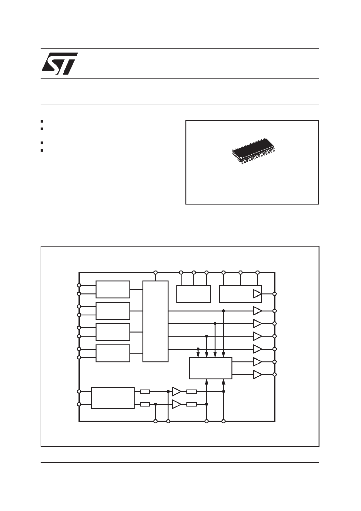
BLOCK DIAGRAM
2
C BUS
TDA7401
SO28
ORDERING NUMBER: TDA7401D
Very low DC stepping is obtained by using a
BICMOStechnology.
HP FL 1
HP FL 2
HP FR 1
HP FR 2
HP RL 1
HP RL 2
HP RR 1
HP RR 2
AUX 1 IN L
AUX 1 IN R
22
21
20
19
18
17
16
15
1
2
HP FILTER
HP FILTER
HP FILTER
HP FILTER
GAIN
+20/-79dB
MUTE
MUTE
45
CR1 CL1 CR2 CL2
SDA SCL DGND AGND CREF V
3
I2C BUS SUPPLY
MUX
76
CC
282324252627
D98AU822A
12
10
11
13
14
9
8
OUT REF
HP FL OUT
HP FR OUT
HP RL OUT
HP RR OUT
AUX 2 OUT L
AUX 2 OUT R
January 1999
1/10

TDA7401
ABSOLUTE MAXIMUM RATINGS
Symbol Parameter Value Unit
V
S
T
amb
T
stg
PIN CONNECTION
Operating Supply Voltage 10.5 V
Operating Ambient Temperature -40 to 85 °C
Storage Temperature Range -55 to 150 °C
AUX 1 IN L
AUX 1 IN R
MUTE
CR1
CL1
CL2
CR2
AUX 2 OUT R
AUX 2 OUT L HP FR 1
HP FL OUT HP FR 2
HP FR OUT
OUT REF
HP RL OUT HP RR 1
1
2
3
4
5
6
7
8
9
10
12
13
28
27
26
25
24
23
22
21
20
19
18
17
16
1514HP RR OUT HP RR 2
D98AU823A
V
CC
SDA
SCL
DGND
AGND
CREF
HP FL 1
HP FL 2
HP RL 111
HP RL 2
THERMAL DATA
Symbol Parameter Value Unit
R
th j-amb
Thermal Resistance Junction-pins 65 °C/W
QUICK REFERENCE DATA
Symbol Parameter Min. Typ. Max. Unit
V
V
CL
THD Total Harmonic Distortion V = 1Vrms f = 1KHz 0.01 0.08 %
S/N Signalto Noise Ratio 106 dB
S
V
REF
2/10
Supply Voltage 6 9 10.2 V
S
Max. input signal handling 2.1 2.6 Vrms
Channel Separation f = 1KHz -80 100 dB
C
Reference Voltage Output (pin 12) 4.2 4.5 4.8 V
TDA7401
ELECTRICALCHARACTERISTICS (VS= 9V; RL= 10KΩ;Rg=50Ω;T
=25°C; all gains= 0dB;
amb
f = 1KHz. Refer to the test circuit,unless otherwisespecified.)
Symbol Parameter Test Condition Min. Typ. Max. Unit
INPUTSTAGE:AUX1
R
V
CL
S
Input Resistance 37.5 50 62.5 KΩ
I
Clipping Level d ≤ 0.3% 2.1 2.6 V
Input Separation 80 100 dB
I
GAIN CONTROL
G
MAX
A
MAX
A
STEP
E
A
E
T
V
DC
Maximum Input Gain 20 dB
Maximum Attenuation 79 dB
Step Resolution 0.5 1 1.5 dB
Attenuation Set Error G = -20 to +20dB -1.25 0 +1.25 dB
G = -60 to -20dB -4 3 dB
Tracking Error 2dB
DC Steps Adiacent Attenuation Steps 0.1 3 mV
From 0dB to G
MIN
0.5 5 mV
AUDIO OUTPUT(Pin 8 - 9, 10 - 14)
V
clip
R
L
R
O
V
DC
Clipping Level d = 0.3% 2.1 2.6 Vrms
Output Load Resistance AC coupled 2 K
Output Impedance 30 100 Ω
DC Voltage Level 4.2 4.5 4.8 V
STAGE:HP FILTER
R1 Resistance at pin HP1 HIGHPASS BYTE = XXXX1000 127.5 170 212.5 K
R2 Resistance at pin HP2 1 MΩ
V
CL
Clipping Level d ≤ 0.3% 2.1 2.6 Vrms
MUTE
A
V
R
MUTE
THM
INT
Mute Attenuation 80 100 dB
Mute Threshold 1.2 1.7 2.2 V
Pullup Resistor (pin3)
(note 1)
37.5 50 62.5 K
GENERAL
V
CC
I
CC
PSRR Power Supply Rejection Ratio f = 1KHz 60 70 dB
e
NO
S/N Signal to NoiseRatio All Gains = 0dB; V
S
C
d Distortion V
Supply Voltage 6 9 10.2 V
Supply Current 7 8 9 mA
Output Noise NonInvertingOutputMuted(B=
3.5 15
20 to 20kHz flat)
All Gains0dB(B=20to20kHz
515µV
flat)
O
=1V
rms
106 dB
Channel Separation 80 100 dB
=1V 0.01 0.08 %
IN
BUS INPUTS
V
IL
V
lH
I
lN
V
O
Note 1: Internal pullup resistor to 3.3V;”LOW” = mute active
Input Low Voltage 0.8 V
Input High Voltage 2.5 V
Input Current VIN= 0.4V -5 5 µA
OutputVoltageSDA
IO= 1.6mA 0.1 0.4 V
Acknowledge
RMS
µ
Ω
Ω
Ω
V
3/10

TDA7401
Figure 1. HP Filter
100nF 100nF
HP2
56.5K
18.7K
9.4K
7.7K
56K
4.4K
3.6K
12.5K
HP1
6.2K 3.5K 2.1K 3.8K 4.7K 9.4K 28K
+
-
Figure 2. ApplicationCircuit
100nF 100nF
HP FL IN
100nF 100nF
HP FR IN
100nF 100nF
HP RL IN
100nF 100nF
HP RR IN
220nF
AUX L IN
AUX R IN
220nF
HP FL 1
HP FL 2
HP FR 1
HP FR 2
HP RL 1
HP RL 2
HP RR 1
HP RR 2
AUX 1 IN L
AUX 1 IN R
22
21
20
19
18
17
16
15
1
2
28K
R1 =EQUIVALENT RESISTANCE AT PIN HP1
R2 =EQUIVALENT RESISTANCE AT PIN HP2
MUTE
3
HP FILTER
HP FILTER
MUTE
HP FILTER
HP FILTER
GAIN
+20/-79dB
45
CR1 CL1 CR2 CL2
100nF
µP
SDA
2
C BUS SUPPLY
I
100 nF100
nF
D98AU836
SCL
DGND
MUX
76
AGND
100nF
10µF
CREF
V
282324252627
100nF
CC
OUT REF12
HP FL OUT10
HP FR OUT11
HP RL OUT13
HP RROUT14
AUX L OUT9
AUX R OUT8
D98AU835
V
CC
10µF
OUT REF
HP FL OUT
HP FR OUT
HP RL OUT
HP RR OUT
AUX L OUT
AUX R OUT
4/10

TDA7401
2
C BUS INTERFACE
I
Data transmission from microprocessor to the
TDA7401 and viceversa takes place thru the 2
wires I
2
C BUS interface, consisting of the two
lines SDA and SCL (pull-up resistors to positive
supply voltage must be externallyconnected).
Data Validity
As shown in fig.2, thedata on the SDA line must
be stableduring the high period of the clock. The
HIGH and LOW state of the data line can only
change when the clock signal on the SCL line is
LOW.
Start and Stop Conditions
As shown in fig.3 a start condition is a HIGH to
LOW transition of the SDA line while SCL is
HIGH. The stop condition is a LOW to HIGH transition of the SDA line while SCL is HIGH.
A STOP conditions must be sent before each
START condition.
Byte Format
Every byte transferred to the SDA line must con-
Figure 3. Data Validity on the I
2
CBUS
tain 8 bits. Each byte must be followed by an acknowledgebit. The MSB is transferredfirst.
Acknowledge
The master(µP) puts a resistive HIGH level on the
SDA line during the acknowledge clock pulse (see
fig. 4). The peripheral (audioprocessor) that acknowledgeshas to pull-down (LOW) the SDA line
during the acknowledge clock pulse, so that the
SDAlineisstable LOWduringthis clockpulse.
The audioprocessor which has been addressed
has to generate an acknowledge after the reception of each byte, otherwise the SDA line remains
at the HIGH level duringthe ninthclockpulsetime.
In this case the master transmitter can generate
theSTOPinformationin orderto abortthe transfer.
Transmissionwithout Acknowledge
Avoiding to detectthe acknowledgeof the audioprocessor, the µP can use a simplier transmission: simply it waits one clock without checking
the slave acknowledging, and sends the new
data.
This approach of course is less protected from
misworking and decreasesthe noise immunity.
Figure 4. Timing Diagram of I2CBUS
2
Figure 5. Acknowledgeon the I
CBUS
5/10

TDA7401
SOFTWARESPECIFICATION
Interface Protocol
The interfaceprotocolcomprises:
A start condition (s)
read/writetransmission)
A subaddressbyte.
A sequence of data (N-bytes+ acknowledge)
A stop condition (P)
A chip address byte,(the LSB bit determines
CHIP ADDRESS SUBADDRESS DATA 1 to DATA n
MSB LSB MSB LSB MSB LSB
S1000101R/W
X X X I X A2 A1 A0
AC K
ACK
DATA
ACK = Acknowledge
S = Start
P = Stop
I = Auto Increment
X = Not used
AUTO INCREMENT
If bit I in the subaddressbyteis set to ”1”, the autoincrementof the subaddressis enabled
SUBADDRESS (receivemode)
ACK
P
MSB LSB
X X X I X D2 D1 D0
0 0 0 Not used
0 0 1 Mode
0 1 0 Gain AUX1 L
0 1 1 Gain AUX1 R
1 0 0 High Pass Filter FL
1 0 1 High Pass Filter FR
1 1 0 High Pass Filter RL
1 1 1 High Pass Filter RR
FUNCTION
6/10

MODE
TDA7401
MSB LSB
D7 D6 D5 D4 D3 D2 D1 D0
0 X High Pass Mute ON
1 High Pass Mute OFF
0 AUX1 InputMute ON
1 AUX1 InputMute OFF
0 AUX2 Inverted Output
1 AUX2 Non Inv. Output
0 0 High Pass Filter Front
0 1 High Pass Filter Rear
1 0 Aux 1 Input
1 1 Mute
0 0 Flat
0 1 120Hz
1 0 80Hz
1 1 50Hz
GAIN AUX1L, AUX1R
MSB LSB
D7 D6 D5 D4 D3 D2 D1 D0
+31dB
1
1
1
1
1
1
0
0
0
0
0
0
0
:
0
0
0
:
0
0
0
0
:
0
0
:
1
1
0
:
0
0
0
:
0
0
0
0
:
0
0
:
0
0
1
:
1
1
0
:
0
0
0
0
:
0
1
:
0
0
1
:
0
0
1
:
0
0
0
0
:
1
0
:
1
1
1
:
0
0
1
:
0
0
0
0
:
1
0
:
1
1
1
:
0
0
1
:
0
0
0
0
:
1
0
:
1
1
1
:
:
:
:
:
:
+17dB
1
+16dB
0
+15dB
1
:
:
+1dB
1
0dB
0
0dB
0
-1dB
1
:
:
-15dB
1
-16dB
0
:
:
-78dB
0
-79dB
1
FUNCTION
AUX 2 Output Selection
AUX1 Low Pass Filter
(C1 = C2 = 100nF)
GAIN AUX1L, R
Mute
X
Note:
software to the maximum value, which is needed for the system.
1
Is is not recommended to use a gain more than 20dB for system performance reason. In general, the max. gain should be limited by
1
X
X
X
X
X
7/10

TDA7401
HIGH PASS FILTERS
MSB LSB
FL, FR, RL, RR
D7 D6 D5 D4 D3 D2 D1 D0
2nd order HP Filter Mode
(C1 = C2 = 100nF)
XXXX0000 f
0001 f
0010 f
0011 f
0100 f
0101 f
0110 f
0111 f
= 40Hz
c
= 60Hz
c
= 80Hz
c
= 100Hz
c
= 120Hz
c
= 150Hz
c
= 180Hz
c
= 220Hz
c
First order HP Flat Mode
1000 f
= 9Hz
c
8/10

TDA7401
DIM.
MIN. TYP. MAX. MIN. TYP. MAX.
A 2.65 0.104
a1 0.1 0.3 0.004 0.012
b 0.35 0.49 0.014 0.019
b1 0.23 0.32 0.009 0.013
C 0.5 0.020
c1 45° (typ.)
D 17.7 18.1 0.697 0.713
E 10 10.65 0.394 0.419
e 1.27 0.050
e3 16.51 0.65
F 7.4 7.6 0.291 0.299
L 0.4 1.27 0.016 0.050
S8°(max.)
mm inch
OUTLINE AND
MECHANICALDATA
SO28
9/10

TDA7401
Information furnished is believed to be accurate and reliable. However, STMicroelectronics assumes no responsibility for the consequences
of use of such information nor for any infringement of patents or other rights of third parties which may result from its use. No license is
granted by implication or otherwise under any patentor patent rights of STMicroelectronics. Specification mentioned in this publication are
subject to change without notice. This publication supersedes and replaces all information previously supplied. STMicroelectronics products
are not authorized for use as critical components in life support devices or systems without express written approval of STMicroelectronics.
The ST logo is a registered trademark of STMicroelectronics
1999 STMicroelectronics – Printed in Italy – All Rights Reserved
STMicroelectronics GROUP OF COMPANIES
Australia - Brazil - Canada - China - France - Germany - Italy - Japan - Korea - Malaysia - Malta - Mexico - Morocco - The Netherlands -
Singapore- Spain - Sweden -Switzerland - Taiwan - Thailand - United Kingdom- U.S.A.
http://www.st.com
10/10
 Loading...