

32W BRIDGECAR RADIO AMPLIFIER
HIGHPOWER CAPABILITY:
40W/3.2Ω EIAJ
32W/3.2Ω @V
26W/4Ω @V
DIFFERENTIAL INPUTS (EITHER SINGLE
ENDED OR DIFFERENTIAL INPUT SIGNAL
ARE ACCEPTED)
MINIMUMEXTERNALCOMPONENTCOUNT:
- NOBOOTSTRAPCAPACITORS
- NOBOUCHEROT CELLS
- INTERNALLYFIXEDGAIN(30dB)
- NOSVRCAPACITOR
ST.-BYFUNCTION (CMOS COMPATIBLE)
PROGRAMMABLETURN-ON/OFF DELAY
NO AUDIBLE POP DURING MUTE AND ST-
BY OPERATIONS
PROTECTIONS:
SHORT CIRCUIT (TO GND, TO V
THE LOAD)
VERYINDUCTIVE LOADS
CHIP OVERTEMPERATURE
LOADDUMP
OPENGND
ESD
S =14.4V,f = 1KHz,d = 10%
S= 14.4V, f = 1KHz, d =10%
ACROSS
S,
TDA7391PD
PRODUCT PREVIEW
PowerSO20
ORDERING NUMBER: TDA7391PD
DESCRIPTION
The TDA7391PD is a BRIDGE class AB audio
power amplifier specially intended for car radio
High Power applications.
The high power capabilitytogether withthe possibility to operate either in DIFFERENTIAL INPUT
MODE or SINGLEENDED INPUT MODE makes
it suitable for boosters and high end car radio
equipments.
The exclusive fully complementary output stage
and the internal fixed gain configuration drop the
externalcomponentcount.
The on board clipping detectorallowseasy implementationof gain compressionsystems.
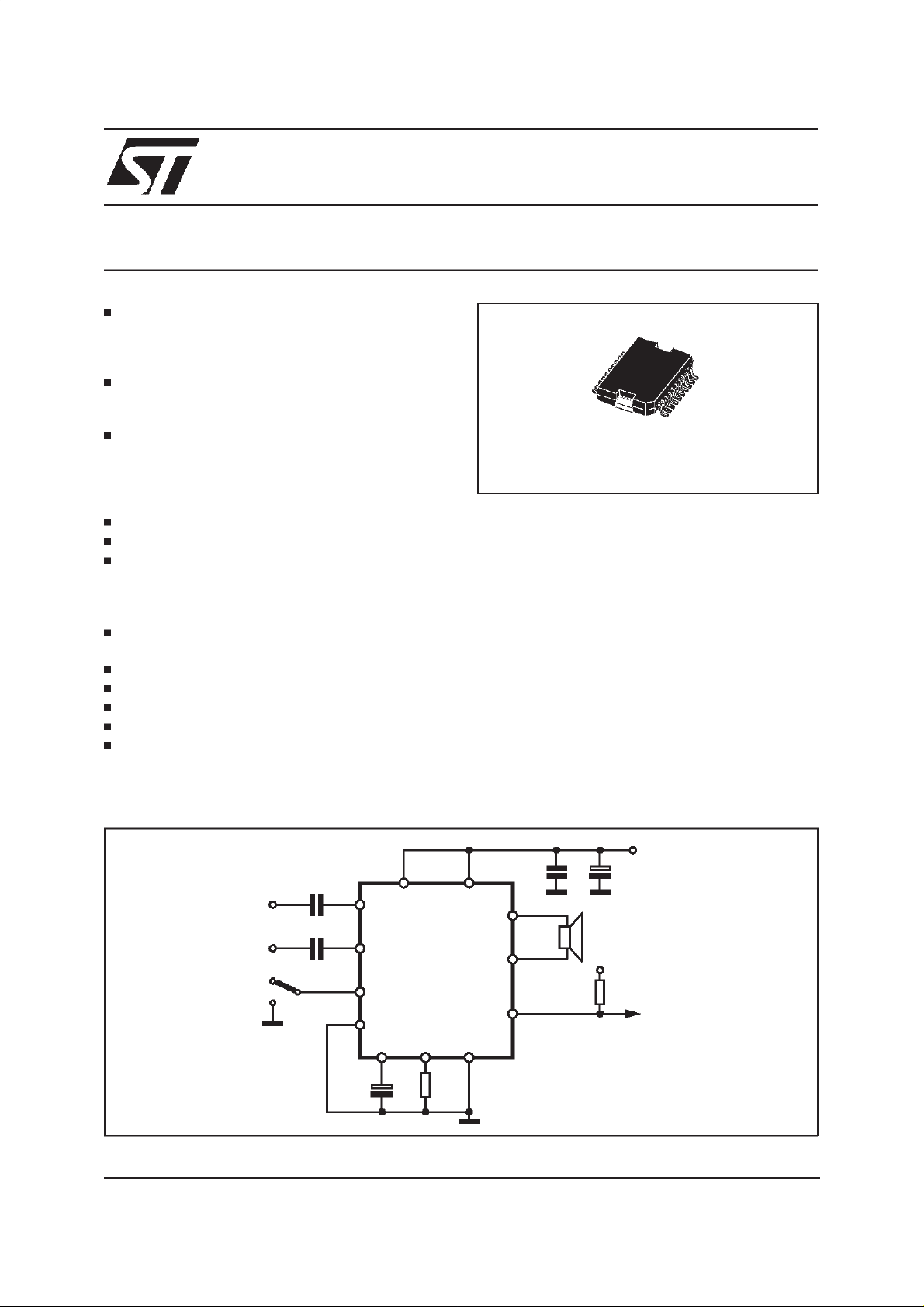
Figure 1: Test AndApplicationCircuit
+V
S
C4 1000µF
Vref
R1
4.7KΩ
TO µC
D98AU871
R2
C5 100nF
2
19
17
GND
OUT+
OUT-
CD
C2 0.22µF
IN+
C1 0.22µF
IN-
V
S
SW1
October 1998
This is preliminaryinformationon anew product now in development. Details are subject tochange without notice.
ST-BY
C3
33µF
516
15
14
TDA7391PD
4
12
9
8 1,10,11,20
56KΩ
1/8

TDA7391PD
Figure 2: BlockDiagram
+
-
STANDBYTHRESHOLD
14
IN-
15
IN+
V
CC1VCC2
516
ICM
gm
+
COMMON
MODE
REFERENCES
-
+
V
CC/2
POWERAMP
LTS V=f (Tj)
POWERAMP
THD
DETECT
SHORT
DUMP &
PROTECTION
V
S
CIRCUIT
THERMAL
L
DISABLE
TS
19
OUT-
17
CD
2
OUT+
+
-
MUTE THRESHOLD
MUTE SYNC S-GND STANDBY
PIN CONNECTION(Topview)
P-GND
OUT+
ST-BY
SYNC
MUTE S-GND
P-GND P-GND
PROGRAMMABLE
CURRENT CIRCUIT
894
N.C.
VCC
N.C.
N.C.
2
3
4
5
6
7
8
9
10
12
20
19
18
17
16
15
14
13
1,10,11,20
P-GND
P-GND1
OUTN.C.
CD
VCC
IN+
INN.C.
D98AU872
12
11
D98AU873
THERMAL DATA
Symbol Description Value Unit
Thermal Resistance Junction-case Max 2 °C/W
2/8
R
th j-case
TDA7391PD
ABSOLUTE MAXIMUM RATINGS
Symbol Parameter Value Unit
V
V
V
PEAK
P
T
stg,Tj
OP
I
O
tot
DC Supply Voltage 28 V
S
Operating Supply Voltage 18 V
Peak Supply Voltage (t= 50ms) 50 V
Output Peak Current repetitive(f > 10Hz)
Output Peak Current non repetitive
Power Dissipation (T
=85°C) 32 W
CASE
4.5
6
Storage and Junction-Case Temperature -40 to 150
A
A
C
°
ELECTRICAL CHARACTERISTICS (VS= 14.4V; RL=4Ω, f = 1KHz, T
=25°C, unless otherwise
amb
specified)
Symbol Parameter Test Condition Min. Typ. Max. Unit
V
S
I
q
V
OS
I
SB
I
SBin
V
SBon
V
SBoff
ATT
ST-BY
I
Min
A
M
P
O
d Distortion
G
V
f
H
R
IN
E
IN
CMRR Input Common Mode Rejection f = 1KHz; V
SVR Supply Voltage Rejection R
CDL Clipping Detection Level 5 10 15 %
T
sd
Supply Voltage Range 8 18 V
Total Quiescent Current 60 150 mA
Output Offset Voltage 120 mV
ST-BY Current V
ST-BY Input Bias Current V
= 1.5V 100
ST-BY
=5V 10
ST-BY
ST-BY On ThresholdVoltage 1.5 V
ST-BY Off thresholdVoltage 3.5 V
ST-BY Attenuation 90 dB
Mute Input BiasCurrent (V
= 5V) 10
MUTE
Mute Attenuation 90 dB
RMS Output Power d = 10%
d=1%
d = 10%;R
EIAJ Output Power V
= 13.7V 40 W
S
= 3.2Ω
L
20 26
21
32
0.06
P
= 0.1 to 15W
O
0.03
Voltage Gain 29.5 30 30.5 dB
High Frequency rolloff PO= 1W; -3dB 75 KHz
Input Impedance Differential 36 60 K
Single Ended 30 55 KΩ
Input Noise Voltage Rg=0Ω;f= 22Hz to 22KHz 4 mV
= 1Vrms 65 dB
IN
=0Ω;Vr= 1Vrms 60 dB
g
Absolute Thermal Shutdown
160
Junction Temperature
A
µ
A
µ
A
µ
W
W
W
%
%
Ω
C
°
3/8

TDA7391PD
FUNCTIONAL DESCRIPTION
Pin Function Description
14,
15
5,16 +V
INPUTS
S
17 CD
2,19 OUTPUTS
1,10,
11,20 P-GND
12 S-GND Signal Ground.
4 STAND-BY
8 SYNC
9 MUTE
The input stage is a high impedance type also capable of operation in single ended mode
with one input capacitively coupled to the signal GND. The impedance seen by the
inverting and non inverting input pins must be matched.
Supply Voltage.
The TDA7391PD is equippedwith a diagnostic circuitryable to detect the clipping in the
Output Signal (distortion= 10%).
The CD pin(open collector)gives out low level signal during clipping.
The output stage isa bridge type able to drive loads as low as 3.2Ω.
It consists of two class AB fully complementary PNP/NPN stages fully protected.
A rail to rail outputvoltage swingis achievedwithout need ofbootstrap capacitors.
No external compensation is necessary.
Power Ground.
The device features aST-BY functionwhich shuts downall the internal bias supplies
when the ST-BY pinis low.
In ST-BY mode the amplifier sinks a small current(in therange of few µA).
When the ST-BY pin ishigh theIC becomes fully operational.
A resistor (R
that flows in the C
) has to beconnect between pin 8and GND in order toprogram the current
2
capacitor (pin 9). Thevalues of C3and R2determine the timerequired
3
to bias the amplifier.
The pin will havea capacitor (C
) tied to GND to set the MUTE/STAND-BY time. An
3
automatic Mute during turn on/off is provided to preventnoisy transients.
4/8

TDA7391PD
Figure 2: Quiescent Current vsSupply Voltage Figure 3: EIAJpower vsSupplyVoltage
Figure 4: OutputPowervs SupplyVoltage
=4Ω)
(@R
L
R
=4
Ω
L
f = 1KHz
RL= 3.2
Ω
R
=4
L
Figure5: Distortionvs Frequency(@ R
V
R
P
Ω
=4Ω)
L
= 14.4V
S
=4
L
= 12W
O
Ω
Figure 6: OutputPowervs SupplyVoltage
=3.2Ω)
(@R
L
R
= 3.2Ω
L
f = 1KHz
f = (Hz)
Figure7: Distortionvs Frequency(R
f = (Hz)
=4Ω)
L
V
R
P
= 14.4V
S
= 3.2
L
= 15W
O
Ω
5/8

TDA7391PD
Figure 8: Supply VoltageRejection vs Frequency Figure9: CommonMode Rejectionvs. Frequency
= 14.4V
V
S
V
= 1Vrms
r
R
=4
L
R
=0
g
Ω
V
V
R
R
S
cm
L
g
= 14.4V
= 1Vrms
=4
Ω
=0
f = (Hz)
Figure 10: TotalPowerDissipation&Efficienc yvs.
(W)
=4Ω)
L
= 14.4V
V
S
R
=4Ω
L
f =1KHz
OutputPower(@R
P
O
f = (Hz)
Figure11: PowerBandwidth
V
= 14.4V
S
R
=4Ω
L
P
=1W
O
f = (Hz)
6/8

TDA7391PD
DIM.
MIN. TYP. MAX. MIN. TYP. MAX.
mm inch
A 3.6 0.142
a1 0.1 0.3 0.004
a2 3.3
0.012
0.130
a3 0 0.1 0.000 0.004
b 0.4 0.53 0.016 0.021
c 0.23 0.32 0.009 0.013
D (1) 15.8 16 0.622 0.630
D1 9.4 9.8 0.370 0.386
E 13.9 14.5 0.547 0.570
e 1.27 0.050
e3 11.43 0.450
E1 (1) 10.9 11.1 0.429 0.437
E2 2.9
0.114
E3 5.8 6.2 0.228 0.244
G 0 0.1 0.000 0.004
H 15.5 15.9 0.610 0.626
h 1.1
0.043
L 0.8 1.1 0.031 0.043
N10°(max.)
S
8°(max.)
T 10 0.394
(1)”D andF” do not include mold flash or protrusions.
- Mold flash or protrusions shallnot exceed 0.15mm (0.006”).
- Critical dimensions: ”E”, ”G” and ”a3”
OUTLINE AND
MECHANICAL DATA
JEDEC MO-166
PowerSO20
E2
hx
45
DETAIL B
BOTTOM VIEW
R
a3
Gage Plane
lead
E
DETAIL B
0.35
S
D1
a1
L
c
DETAIL A
slug
-C-
SEATING PLANE
GC
(COPLANARITY)
E3
NN
a2
A
b
DETAIL A
e3
H
D
T
1
e
1120
E1
10
PSO20MEC
7/8

TDA7391PD
Informationfurnishedis believedto be accurate andreliable. However, STMicroelectronicsassumes noresponsibilityfor the consequenc es
of use of such informationnor forany infringement of patents or otherrights of thirdparties whichmay result from its use. No license is
granted by implicationor otherwise under any patentor patent rights of STMicroelectronics. Specification mentionedin thispublicationare
subjectto change withoutnotice. Thispublicationsupersedes and replacesallinformation previously supplied.STMicroelectronicsproducts
are notauthorizedfor use as criticalcomponentsinlifesupportdevices or sys tems without express writtenapprovalof STMicroelectronics.
Australia - Brazil- Canada - China - France - Germany- Italy - Japan -Korea - Malaysia -Malta - Mexico - Morocco - The Netherlands-
Singapore - Spain - Sweden - Switzerland - Taiwan - Thailand - United Kingdom - U.S.A.
TheST logois a registeredtrademark of STMicroelectronics
1998STMicroelectronics – Printedin Italy – All Rights Reserved
STMicroelectronics GROUP OF COMPANIES
http://www.st.com
8/8
 Loading...