

TDA7382
4 x 22W FOUR BRIDGE CHANNELS CAR RADIO AMPLIFIER
HIGHOUTPUTPOWERCAPABILITY:
4 x30W max./4Ω EIAJ
4 x22W/4Ω@ 14.4V, 1KHz, 10%
4 x18.5W/4Ω@ 13.2V,1KHz, 10%
CLIPPINGDETECTOR(THD =10%)
LOW DISTORTION
LOW OUTPUTNOISE
ST-BYFUNCTION
MUTEFUNCTION
AUTOMUTEAT MIN. SUPPLY VOLTAGE DE-
TECTION
LOW EXTERNALCOMPONENTCOUNT:
– INTERNALLYFIXED GAIN (26dB)
– NOEXTERNAL COMPENSATION
– NOBOOTSTRAP CAPACITORS
PROTECTIONS:
OUTPUT SHORT CIRCUIT TO GND, TO V
ACROSS THE LOAD
VERYINDUCTIVE LOADS
OVERRATING CHIP TEMPERATURE WITH
SOFT THERMALLIMITER
LOADDUMP VOLTAGE
FORTUITOUSOPEN GND
ORDERING NUMBER: TDA7382
REVERSEDBATTERY
ESD PROTECTION
DESCRIPTION
The TDA7382 is a new technology class AB
Audio Power Amplifier in Flexiwatt 25 package
,
S
designed for high end car radioapplications.
Thanks to the fully complementaryPNP/NPN output configuration the TDA7382 allows a rail to rail
output voltage swing with no need of bootstrap
capacitors. The extremely reduced components
count allows very compact sets. The on-board
clipping detector simplifies gain compression operations.
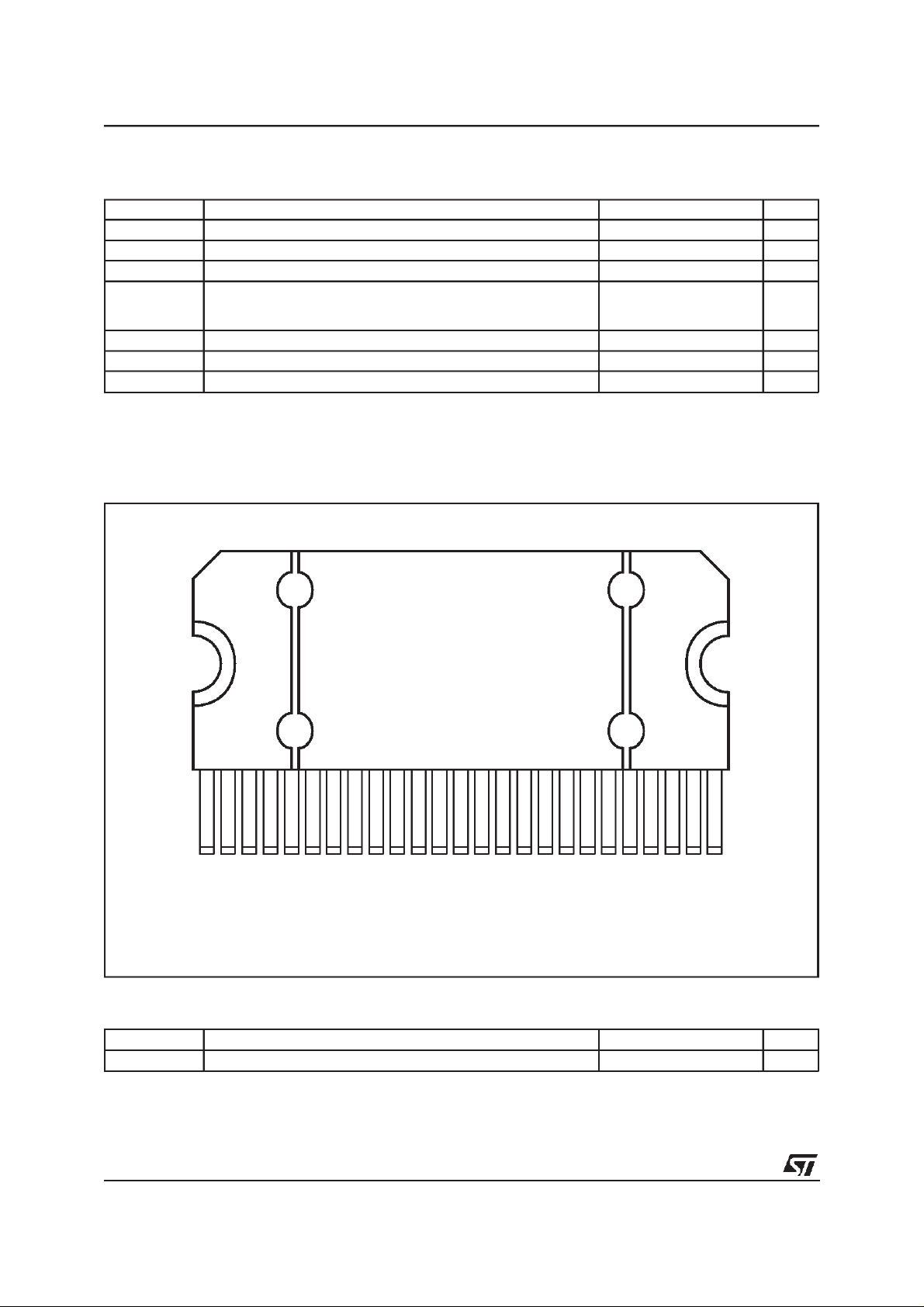
FLEXIWATT25
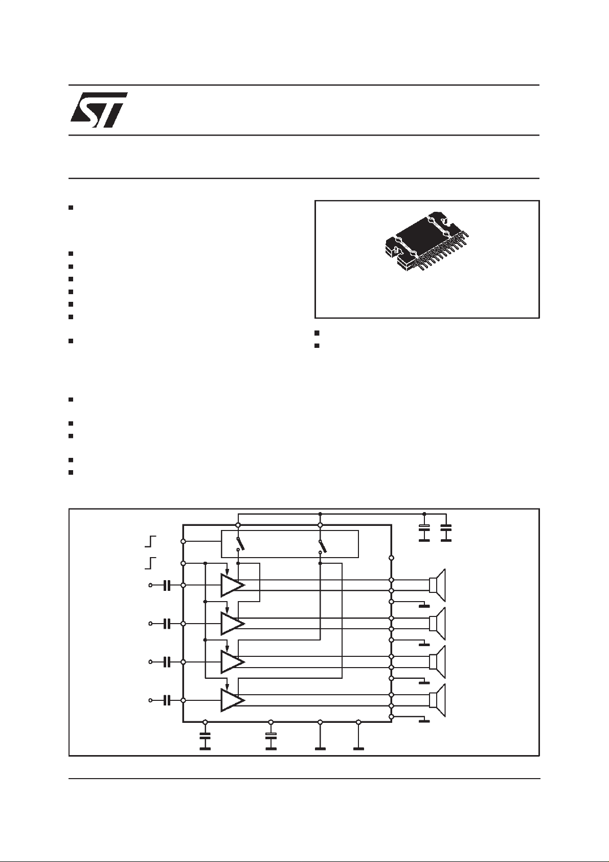
BLOCK AND APPLICATION DIAGRAM
Vcc1 Vcc2
ST-BY
MUTE
IN1
0.1µF
IN2
0.1µF
IN3
0.1µF
IN4
0.1µF
AC-GND
0.1µF47µF
September 1999
100nF2.200µF
CLIPPING DET.
OUT1+
OUT1PW-GND
OUT2+
OUT2PW-GND
OUT3+
OUT3PW-GND
OUT4+
OUT4PW-GND
SVR TAB S-GND
D98AU818
1/10
TDA7382
ABSOLUTE MAXIMUM RATINGS
Symbol Parameter Value Unit
V
CC
V
CC (DC)
V
CC (pk)
I
O
P
tot
T
j
T
stg
PIN CONNECTION (Topview)
Operating Supply Voltage 18 V
DC Supply Voltage 28 V
Peak Supply Voltage (t = 50ms) 50 V
Output Peak Current:
Repetitive (Duty Cycle 10% at f = 10Hz)
Non Repetitive(t = 100µs)
Power dissipation, (T
=70°C) 80 W
case
4.5
5.5
Junction Temperature 150
Storage Temperature – 55 to150 °C
A
A
C
°
1 25
TAB
OUT2-
P-GND
ST-BY
OUT2+
V
CC
OUT1-
P-GND1
SVR
OUT1+
IN1
IN2
IN4
S-GND
IN3
OUT3+
AC-GND
OUT3-
P-GND3
V
CC
MUTE
OUT4+
D98AU820
OUT4-
P-GND4
CLIP. DET.
THERMAL DATA
Symbol Parameter Value Unit
Thermal Resistance Junction to Case Max. 1
2/10
R
th j-case
C/W
°
TDA7382
ELECTRICALCHARACTERISTICS(VS= 14.4V; f = 1KHz; Rg= 600Ω;RL=4Ω;T
amb
=25°C;
Refer to the Testand applicationcircuit (fig.1), unless otherwisespecified.)
Symbol Parameter Test Condition Min. Typ. Max. Unit
I
q1
V
OS
G
v
P
o
P
o max
THD Distortion P
e
No
SVR Supply Voltage Rejection f = 100Hz 50 65 dB
f
cl
f
ch
R
C
T
I
SB
V
SB out
V
SB IN
A
M
V
M out
V
Min
I
m (L)
CDL Clipping Detection THD Level 5 10 15 %
Quiescent Current 85 180 300 mA
Output Offset Voltage 100 mV
Voltage Gain 25 26 27 dB
Output Power THD = 10%
THD = 1%
THD = 10%; V
THD = 10%; V
THD = 5%; V
THD = 1%; V
THD = 10%; V
THD = 1%; V
= 13.5V
S
= 14V
S
= 14V
S
= 14V
S
= 13.2V
S
= 13.2V
S
20
16.5
17
19
17
16
17
14
22
18
20
21
19
17
18.5
15
Max. Output Power EIAJ RULES 27.5 30 W
= 4W 0.04 0.3 %
o
Output Noise ”A” Weighted
Bw = 20Hz to 20KHz
50
65
Low Cut-Off Frequency 20 Hz
High Cut-Off Frequency 75 KHz
Input Impedance 60 100 130 KΩ
i
Cross Talk f = 1KHz 50 70 dB
St-By Current Consumption St-By = LOW 20 100 µA
St-By OUT ThresholdVoltage (Amp: ON) 3.5 V
St-By IN Threshold Voltage (Amp: OFF) 1.5 V
Mute Attenuation VO= 1Vrms 80 90 dB
Mute OUT Threshold Voltage (Amp: Play) 3.5 V
Mute IN Threshold Voltage (Amp: Mute) 1.5 V
Muting Pin Current V
MUTE
= 1.5V
51316
(Source Current)
120
150
W
W
W
W
W
W
W
W
µV
V
µ
A
µ
3/10

TDA7382
Figure 1: StandardTest and Application Circuit
ST-BY
MUTE
IN1
IN2
IN3
IN4
R1
10K
R2
47K
C1
0.1µF
C2 0.1µF
C3 0.1µF
C4 0.1µF
C9
1µF
C10
1µF
S-GND
C8
0.1µF
4
22
11
12
15
14
13
16 10 25 1
C5
0.1µF
C7
2200µF
Vcc1-2 Vcc3-4
SVR TAB
C6
47µF
620
9
8
7
5
2
3
17
18
19
21
24
23
OUT1
OUT2
OUT3
OUT4
D98AU819
4/10
CLIPPING DET.

Figure 2: P.C.B. and componentlayout of the figure 1 (1:1scale)
TDA7382
COMPONENTS &
TOP COPPER LAYER
TDA7382
BOTTOM COPPER LAYER
5/10

TDA7382
Figure 3: QuiescentCurrent vs. Supply Voltage
Figure4: Quiescent Output Voltage vs. Supply
Voltage
Figure 5: Output Power vs. SupplyVoltage Figure6: Distortionvs. Output Power
Figure 7: Distortion vs. Frequency.
6/10
Figure 8: Supply Voltage Rejection vs.
Frequencyby varyingC6
Rg= 600
V
ripple
Ω
= 1Vrms

TDA7382
Figure 9: Output Noise vs. Source Resistance Figure10: Power Dissipation & Efficiency vs.
(W)
tot
OutputPower
P
tot
P
Rg(Ω)
INPUT STAGE
The TDA7382’S inputs are ground-compatible
and can stand very high input signals (± 8Vpk)
without any performancesdegradation.
If the standard value for the input capacitors
(0.1µF) is adopted, the low frequency cut-off will
amount to 16 Hz.
STAND-BYAND MUTING
STAND-BY and MUTING facilities are both
CMOS-COMPATIBLE. If unused, a straight connection to Vs of theirrespective pins wouldbe admissible. Conventionallow-power transistors can
be employed to drive muting and stand-by pins in
Figure 11: Input/OutputBiasing.
100KΩ
F
0.1µ
C1 ÷ C4
IN
absence of true CMOS ports or microprocessors.
R-C cells have always to be used in order to
smooth down the transitions for preventing any
audibletransient noises.
Since a DC current of about 10 uA normally flows
out of pin 22, the maximum allowable muting-series resistance (R
) is 70KΩ, which is sufficiently
2
high to permit a muting capacitor reasonably
small(about 1µF).
If R
is higher than recommended, the involved
2
risk will be that the voltage at pin 22 may rise to
above the 1.5 V threshold voltage and the device
will consequently fail to turn OFF when the mute
line is brought down.
About the stand-by, the time constant to be as-
+
-
8KΩ
400Ω
V
S
10KΩ
10KΩ
SVR AC_GND
100KΩ70KΩ
47µ
C6
F
0.1µ
C5
F
400Ω
8KΩ
-
+
TOWARDS
OTHER CHANNELS
D95AU302
7/10

TDA7382
signed in order to obtain a virtually pop-free transition has to be slowerthan 2.5V/ms.
CLIPPING DETECTOR
The CLIPPING DETECTOR acts in a wayto out-
put a signal as soon as one or more outputs
reachor trespassa typical THD level of 10%.
As a result, the clipping-related signal at pin 25
takes the form of pulses, which are syncronized
with each single clipping event in the music program. Applications making use of this facility
usually operatea filtering/integrationof thepulses
train through passive R-C networks and realize a
volume (or tone bass) stepping down in association with microprocessor-drivenaudioprocessors.
The maximum load that pin 25 can sustain is
Figure 12: Diagnosticscircuit.
Vpin 25
R
D97AU810
VREF
25
TDA7382
1KΩ.
Due to its operating principles, the clipping detec-
tor has to be viewed mainly as a power-dependent feature rather than frequency-dependent.This
means that clipping state causing THD = 10%
typ. will be immediately signaled out whenever a
fixed power level is reached, regardless of the
audiofrequency.
In other words, this feature offers the means to
counteract the extremely sound-damaging effects
of heavy clipping,caused by a suddenincrease of
odd order harmonics and appearance of serious
intermodulationphenomena.
Figure13: Clipping Detection Waveforms.
VO
ICLIP
0
AUDIO
OUTPUT
SIGNAL
D97AU811
CLIPPING
DET.
OUTPUT
CURR.
time
Figure 14: DiagnosticsWaveforms.
PIN
ST-BY
VOLTAGE
PIN
MUTE
VOLTAGE
Vs
OUTPUT
WAVEFORM
25
Vpin
WAVEFORM
CLIPPING
t
t
t
t
D97AU812A
8/10

TDA7382
DIM.
MIN. TYP. MAX. MIN. TYP. MAX.
mm inch
A 4.45 4.50 4.65 0.175 0.177 0.183
B 1.80 1.90 2.00 0.070 0.074 0.079
C 1.40 0.055
D 0.75 0.90 1.05 0.029 0.035 0.041
E 0.37 0.39 0.42 0.014 0.015 0.016
F (1) 0.57 0.022
G 0.80 1.00 1.20 0.031 0.040 0.047
G1 23.75 24.00 24.25 0.935 0.945 0.955
H (2) 28.90 29.23 29.30 1.138 1.150 1.153
H1 17.00 0.669
H2 12.80 0.503
H3 0.80 0.031
L (2) 22.07 22.47 22.87 0.869 0.884 0.904
L1 18.57 18.97 19.37 0.731 0.747 0.762
L2 (2) 15.50 15.70 15.90 0.610 0.618 0.626
L3 7.70 7.85 7.95 0.303 0.309 0.313
L4 5 0.197
L5 3.5 0.138
M 3.70 4.00 4.30 0.145 0.157 0.169
M1 3.60 4.00 4.40 0.142 0.157 0.173
N 2.20 0.086
O 2 0.079
R 1.70 0.067
R1 0.5 0.02
R2 0.3 0.12
R3 1.25 0.049
R4 0.50 0.019
V5°(Typ.)
V1 3° (Typ.)
V2 20°(Typ.)
V3 45°(Typ.)
(1): dam-bar protusion not included
(2): molding protusion included
OUTLINE AND
MECHANICAL DATA
Flexiwatt25
L2
H
V3
OL3 L4
V
C
H3
G
H1
G1
R3
H2
F
A
R4
N
V2
R2
R
L
L1
V1
R2
B
V
FLEX25ME
L5
R1
R1 R1
V1
D
E
M1
M
9/10

TDA7382
Information furnished is believed to be accurate and reliable. However, STMicroelectronics assumes no responsibility for the consequences
of use of such information nor for any infringement of patents or other rights of third parties which may result from its use. No license is
granted by implication or otherwise under any patent or patent rights of STMicroelectronics. Specification mentioned in this publication are
subject to change without notice. This publication supersedes and replaces all information previously supplied. STMicroelectronics products
are not authorized for use as critical components in life support devices or systems without express written approval of STMicroelectronics.
The ST logo is a registered trademark of STMicroelectronics
1999 STMicroelectronics – Printed in Italy – All Rights Reserved
STMicroelectronics GROUP OF COMPANIES
Australia - Brazil - China - Finland - France - Germany - Hong Kong - India - Italy - Japan - Malaysia - Malta - Morocco -
Singapore - Spain - Sweden - Switzerland - United Kingdom - U.S.A.
http://www.st.com
10/10
 Loading...