

SGS Thomson Microelectronics TDA7375AV, TDA7375AH Datasheet
TDA7375A
2 x 37WDUAL/QUAD POWER AMPLIFIER FOR CAR RADIO
HIGHOUTPUTPOWER CAPABILITY
2
x 43W/4Ω MAX
2
x 37W/4
2
x 26W/4
x 7W/4Ω @14.4V,1KHz,10%
4
4
x 12W/2Ω @14.4V, 1KHz,10%
MINIMUM EXTERNAL COMPONENTS
COUNT:
– NOBOOTSTRAPCAPACITORS
– NOBOUCHEROTCELLS
– INTERNALLY FIXEDGAIN (26dBBTL)
ST-BYFUNCTION(CMOSCOMPATIBLE)
NO AUDIBLE POP DURING ST-BY OPERA-
TIONS
DIAGNOSTICFACILITIES
– CLIPDETECTOR
– OUTTO GND SHORT
– OUTTO V
– SOFTSHORTAT TURN-ON
– THERMAL SHUTDOWNPROXIMITY
Protections:
OUPUTAC/DC SHORT CIRCUIT
– TOGND
EIAJ
Ω
@14.4V,1KHz,10%
Ω
SHORT
S
Multiwatt15 V
ORDERING NUMBERS: TDA7375AV
–TOV
S
TDA7375AH
– ACROSS THE LOAD
SOFTSHORT AT TURN-ON
OVERRATING CHIP TEMPERATURE WITH
SOFTTHERMAL LIMITER
LOADDUMP VOLTAGESURGE
VERYINDUCTIVELOADS
FORTUITOUSOPEN GND
REVERSEDBATTERY
ESD
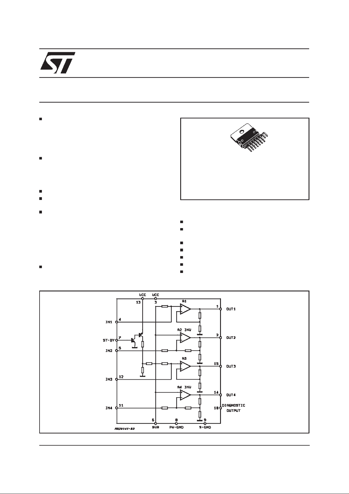
BLOCK DIAGRAM
October 1998
1/14
TDA7375A
DESCRIPTION
The TDA7375A is a new technology class AB car
radio amplifier able to work either in DUAL
BRIDGEor QUADSINGLE ENDED configuration.
The exclusive fully complementarystructureof the
output stage and the internally fixed gain guaran-
tee the highest power performances with extremely reduced component count. The on board
clip detector simplifies gain compression operation. The fault diagnostic makes it possible to detect mistakes during car radio set assembly and
wiring in the car.
GENERALSTRUCTURE
ABSOLUTEMAXIMUM RATINGS
Symbol Parameter Value Unit
V
op
V
V
peak
I
O
I
O
P
tot
T
stg,Tj
Operating Supply Voltage 18 V
DC Supply Voltage 28 V
S
Peak Supply Voltage(for t = 50ms) 40 V
Output Peak Current (notrepitive t = 100µs) 4.5 A
Output Peak Current (repetitivef > 10Hz) 3.5 A
Power Dissipation T
Storage and Junction Temperature -40 to 150 °C
=85°C36W
case
THERMAL DATA
Symbol Description Value Unit
R
th j-case
Thermal Resistance Junction-case Max 1.8 °C/W
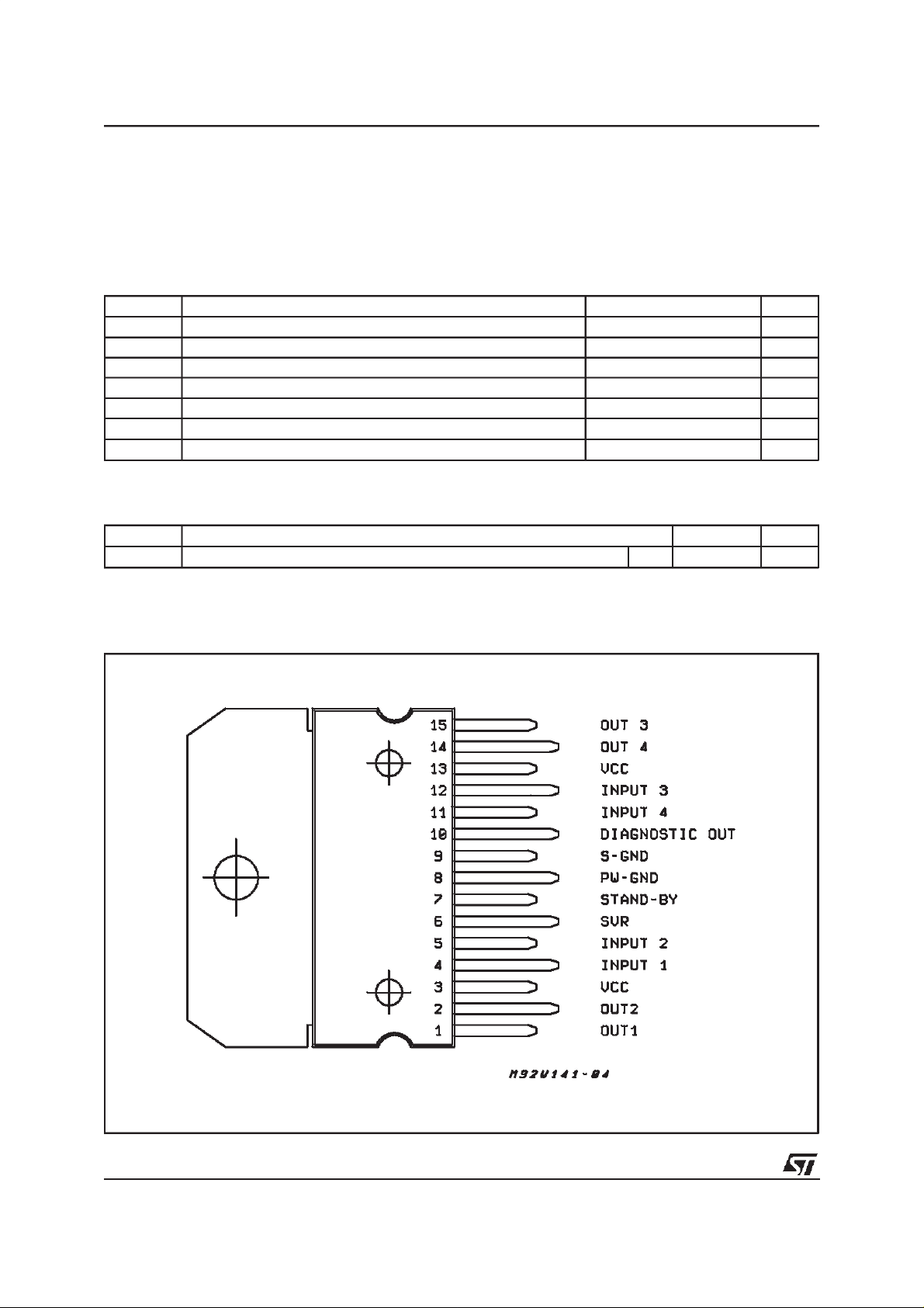
PIN CONNECTION (Topview)
2/14
TDA7375A
ELECTRICALCHARACTERISTICS (Referto the testcircuit, VS=14.4V;RL=4Ω; f =1KHz;
T
=25°C,unless otherwise specified
amb
Symbol Parameter Test Condition Min. Typ. Max. Unit
V
S
I
d
V
OS
P
O
P
O max
P
O EIAJ
THD Distortion R
CT Cross Talk f = 1KHz Single Ended
R
IN
G
V
G
V
E
IN
SVR Supply Voltage Rejection R
A
SB
I
SB
V
SB
V
SB
I
pin7
I
cd off
I
cd on
V
sat pin10
(*) See built-in S/C protection description
(**) Pin 10 Pulled-up to 5V with 10KΩ;R
(***) Saturatedsquare waveoutput.
Supply Voltage Range 8 18 V
Total Quiescent DrainCurrent RL= ∞ 150 mA
Output Offset Voltage 150 mV
Output Power THD = 10%; RL=4
Bridge
Single Ended
Single Ended, R
Ω
23
6.5
=2
Ω
L
26
7
12
Max. Output Power (***) VS = 14.4V,Bridge 37 43 W
EIAJ Output Power (***) VS= 13.7V, Bridge 33 37 W
=4Ω
L
Single Ended, P
Bridge, P
O
= 0.1 to 4W
O
= 0.1 to10W
0.02
0.03 0.3
70
f = 10KHzSingle Ended
f = 1KHz Bridge
f = 10KHzBridge
Input Impedance Single Ended
Bridge
Voltage Gain Single Ended
Bridge
55
20
10
19
25
60
60
30
15
20
26
21
27
Voltage Gain Match 0.5 dB
Input Noise Voltage Rg= 0; ”A”weighted, S.E.
Non Inverting Channels
Inverting Channels
2
5
Bridge
Rg = 0;22Hz to 22KHz 3.5 µV
= 0; f = 300Hz 50 dB
g
Stand-by Attenuation PO=1W 80 90 dB
ST-BY Current Consumption V
= 0 to1.5V 100
ST-BY
ST-BY In ThresholdVoltage 1.5 V
ST-BY Out ThresholdVoltage 3.5 V
ST-BY Pin Current Play ModeV
Max Driving Current Under
=5V 50 µA
pin7
5mA
Fault (*)
Clipping Detector
d = 1%(**) 90
Output Average Current
Clipping Detector
d = 5%(**) 160 µA
Output Average Current
Voltage Saturation on pin10 Sink Currentat Pin 10= 1mA 0.7 V
=4Ω
L
W
W
W
%
%
dB
dB
dB
dB
K
KΩ
dB
dB
µV
µV
µ
µ
Ω
A
A
3/14
TDA7375A
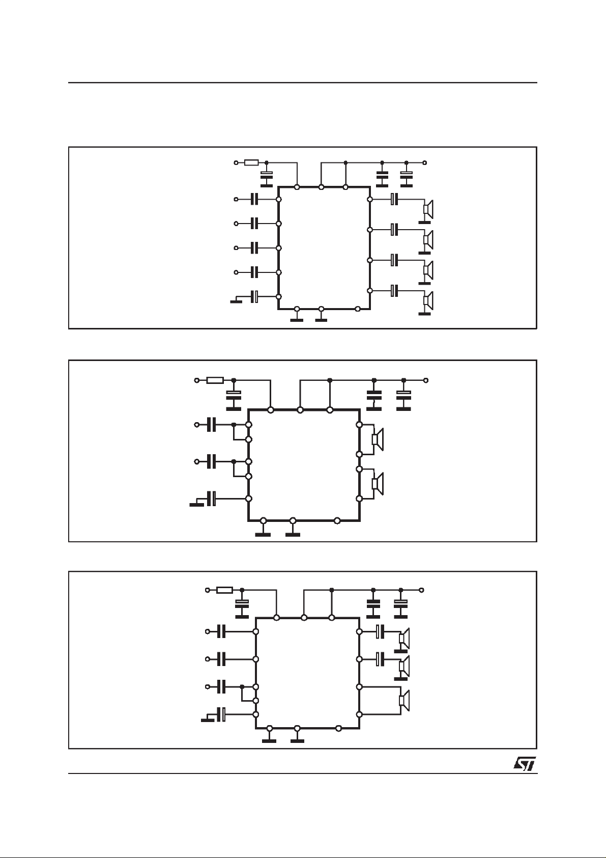
STANDARD TEST AND APPLICATION CIRCUIT
Figure 1: Quad Stereo
Note:
The output decoupling capaci t or s
(C9,C10,C11,C12)could bereducedto
1000µFifthe2Ωoperation is not
required.
Figure 2: Double Bridge
ST-BY
IN L
ST-BY
IN FR 5
IN RR 11
10K R1
IN FL
C1 0.22µF
C2 0.22µF
C4 0.22µF
C3 0.22µF
C8 47µF
10K R1
C5
10µF
C1 0.47µF
C2 0.47µF
C8 47µF
C7
10µF
7
13
4
12IN RL
6
89 10
3
DIAGNOSTICS
C4
100nF
13
7
4
3
1
5
12IN R
11
6
2
15
14
89 10
DIAGNOSTICS
C6
100nF
1
2
15
14
C10 2200µF
C9 2200µF
C11 2200µF
C12 2200µF
D94AU063A
OUT L
OUT R
D94AU064A
V
S
C5
1000µF
V
C3
1000µF
OUT FL
OUT FR
OUT RL
OUT RR
S
Figure 3: Stereo/Bridge
IN BRIDGE 12
4/14
ST-BY
IN L
IN L
10K
0.22µF
0.22µF
0.47µF
47µF
10µF
13
7
4
3
5
11
6
89 10
DIAGNOSTICS
15
14
1
2
2200µF
2200µF
D94AU065A
1000µF100nF
OUT L
OUT R
OUT
BRIDGE
V
S
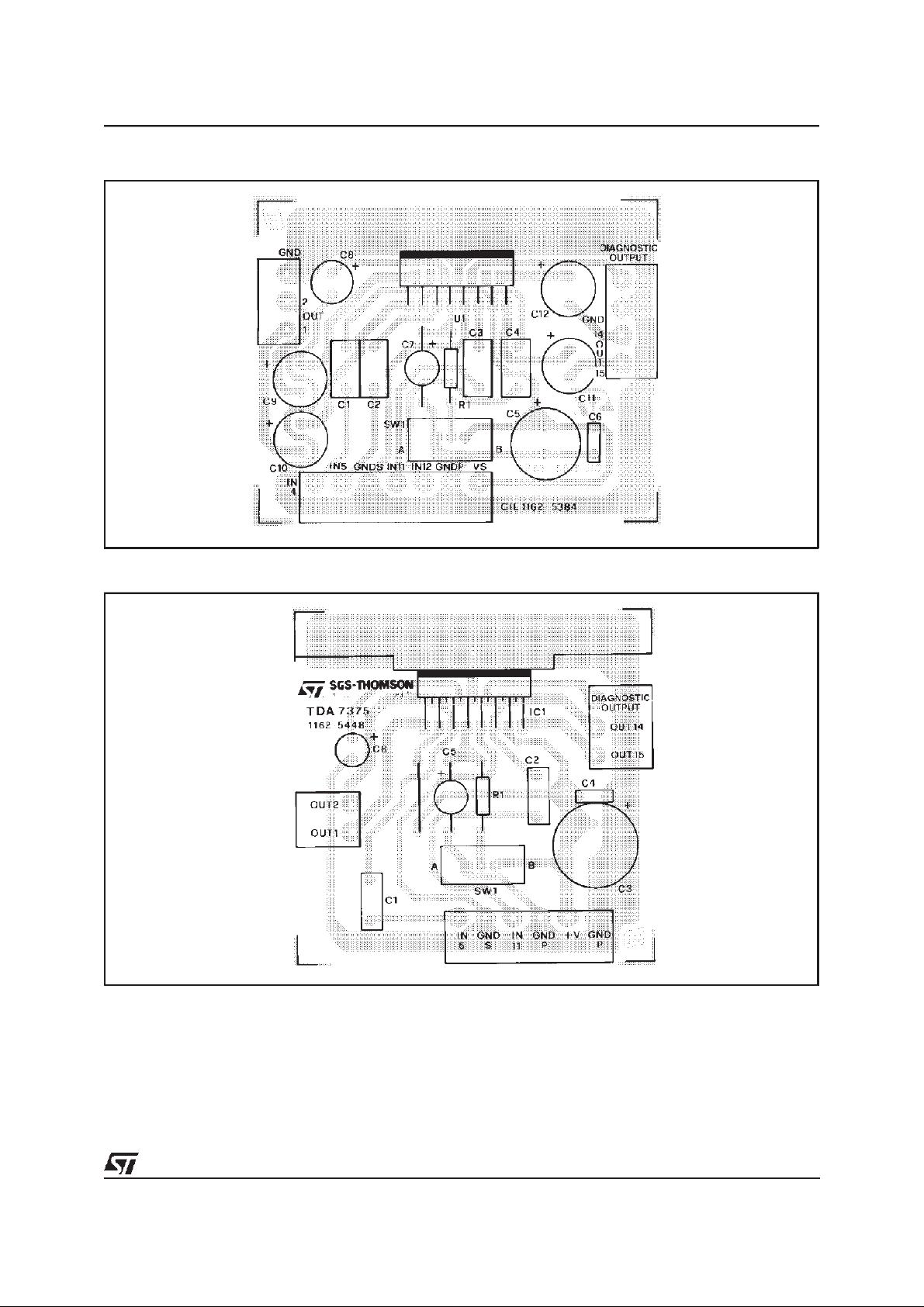
Figure 4: P.C. Board and ComponentLayout of the fig.1(1:1 scale).
TDA7375A
Figure 5: P.C. Board and ComponentLayout of the fig.2(1:1 scale).
5/14
 Loading...