

QUAD POWER AMPLIFIER FOR CAR RADIO
MINIMUMEXTERNAL COMPONENTCOUNT
HIGHCURRENT CAPABILITY
NO BOOTSTRAPCAPACITORS
NO BOUCHEROTCELLS
CLIP DETECTOR OUTPUT
HIGHOUTPUT POWER
HIGHAPPLICATIONFLEXIBILITY
FIXED GAIN
VERYLOW STAND-BYCURRENT (1µA typ)
NO SWITCH ON/OFF NOISE
PROTECTIONS:
OUTPUT AC/DC SHORT CIRCUIT TO GND
ANDTO V
VERYINDUCTIVE LOADS
OVERRATINGCHIP TEMPERATURE
LOADDUMP VOLTAGE
FORTUITOUS OPEN GND
REVERSEBATTERY
ESD
S
TDA7370
MULTIWATT15
ORDERING NUMBER: TDA7370
DESCRIPTION
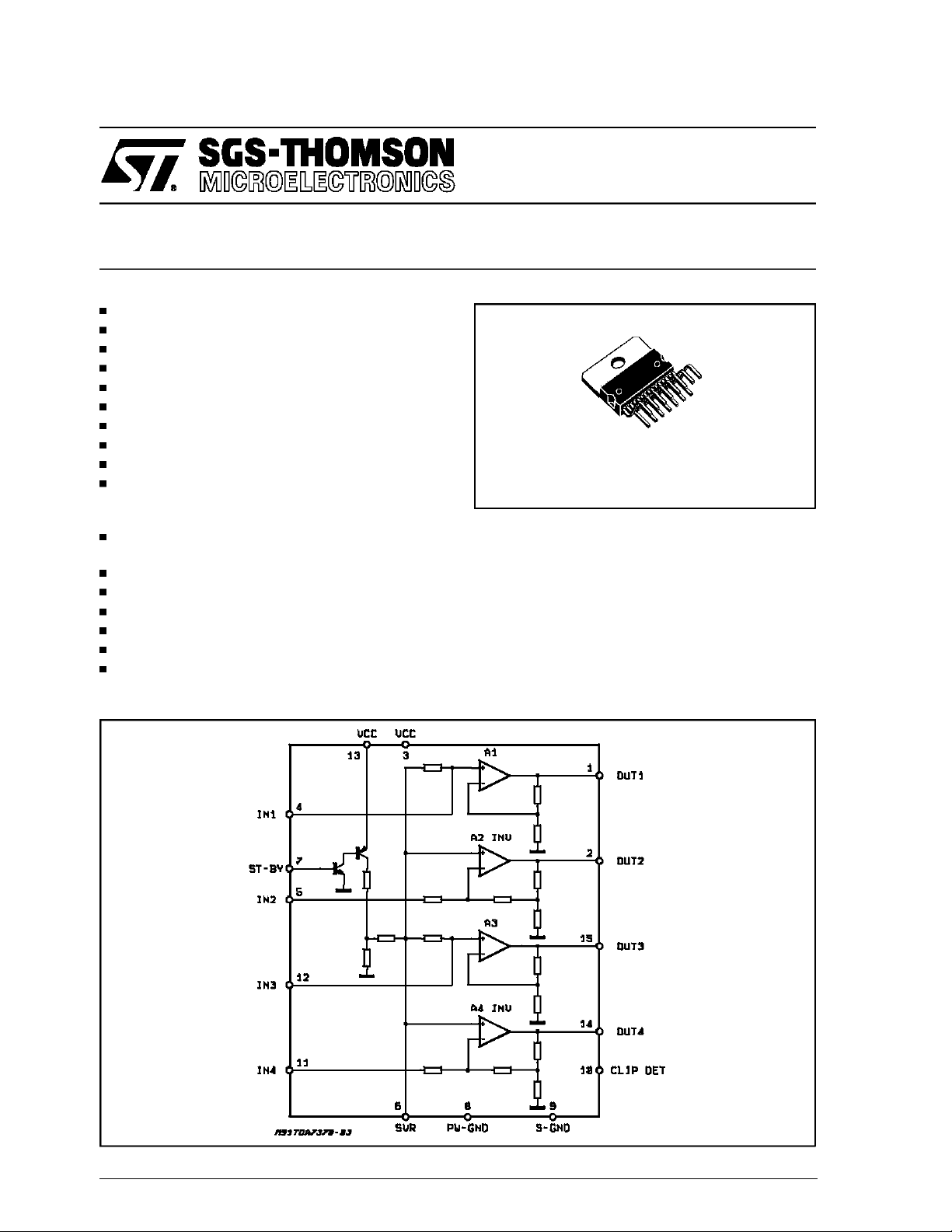
The TDA7370 is a newtechnologyclass AB quad
channelsAudioPower Amplifier in Multiwattpackage designed for carradio applications.
Thanks to the fully complementaryPNP/NPNoutput configuration the high power performances of
the TDA7370 are obtained without bootstrap capacitors.
BLOCK DIAGRAM
April 1995
1/17
TDA7370
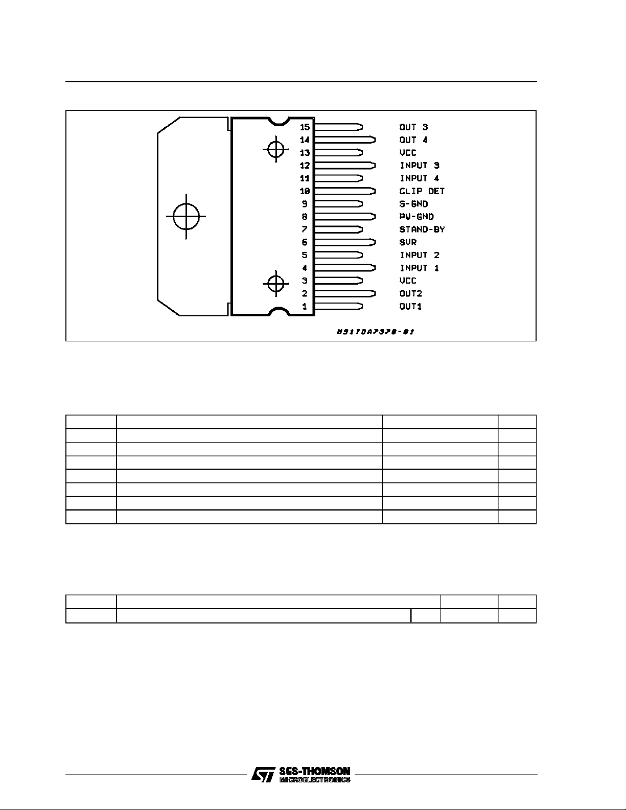
PIN CONNECTION(Top view)
ABSOLUTE MAXIMUM RATINGS
Symbol Parameter Value Unit
V
V
V
PEAK
P
T
stg,Tj
I
I
DC Supply Voltage 28 V
S
Operating Supply Voltage 18 V
OP
Peak Supply Voltage (t = 50ms) 50 V
Output Peak Current (not rep. t = 100µs) 4.5 A
O
Output Peak Current (rep. f > 10Hz) 3.5 A
O
Power Dissipation (T
tot
=85°C) 36 W
case
Storage and Junction Temperature -40 to 150 °C
THERMAL DATA
Symbol Description Value Unit
R
th j-case
Thermal Resistance Junction-case Max 1.8 °C/W
2/17

TDA7370
ELECTRICAL CHARACTERISTICS (Refer to the test circuit;VS=14.4V; RL=4Ω,T
amb
=25°C,
f = 1kHz, unless otherwise specified)
Symbol Parameter Test Condition Min. Typ. Max. Unit
V
S
I
d
P
O
d Distortion R
CT Cross Talk f = 1kHz Bridge
R
IN
G
V
G
V
E
IN
SVR Supply Voltage Rejection R
ASB Stand-by Attenuation 60 dB
I
SB
V
SB ON
V
SB OFF
V
OS
I
CD OFF
I
CD ON
(*) Weighted A
(**) Pin 10Pulled-up to 5V with 10kΩ;
Supply Range 8 18 V
Total Quiescent Drain Current RL= ∞ 150 mA
Output Power RL=4Ω; THD = 10%
Single Ended
Bridge
=4Ω;
L
Single Ended, P
Bridge, P
= 0.1 to 10W 0.03
O
= 0.1 to 4W
O
5.5 6.5
20
0.5 %
65
f = 10kHz Bridge
f = 1kHz Single Ended
f = 10kHz Single Ended
Input Impedance Single Ended
Bridge
Voltage Gain Single Ended
Bridge
20
55
60
50
15
20
26
Voltage Gain Match. 1 dB
Input Noise Voltage (*) SINGLE ENDED
Non Inv. Ch., R
Inv. Ch., R
BRIDGE (R
= 0; f = 100Hz to 10kHz 50 dB
g
= 10kΩ
g
= 10kΩ
g
= 0 to 10kΩ)
g
3.0
5
3.5
ST-BY Current 1 µA
ST-BY On Threshold Voltage 1.5 V
ST-BY Off Threshold Voltage 3.5 V
Output Offset Voltage 200 mV
ClippingDetector ”OFF”
Output Average Current
ClippingDetector ”ON”
Output Average Current
THD = 1% (**)
100 µA
THD = 10% (**)
190 µA
W
W
%
dB
dB
dB
dB
KΩ
KΩ
dB
dB
µV
µV
µV
3/17
TDA7370
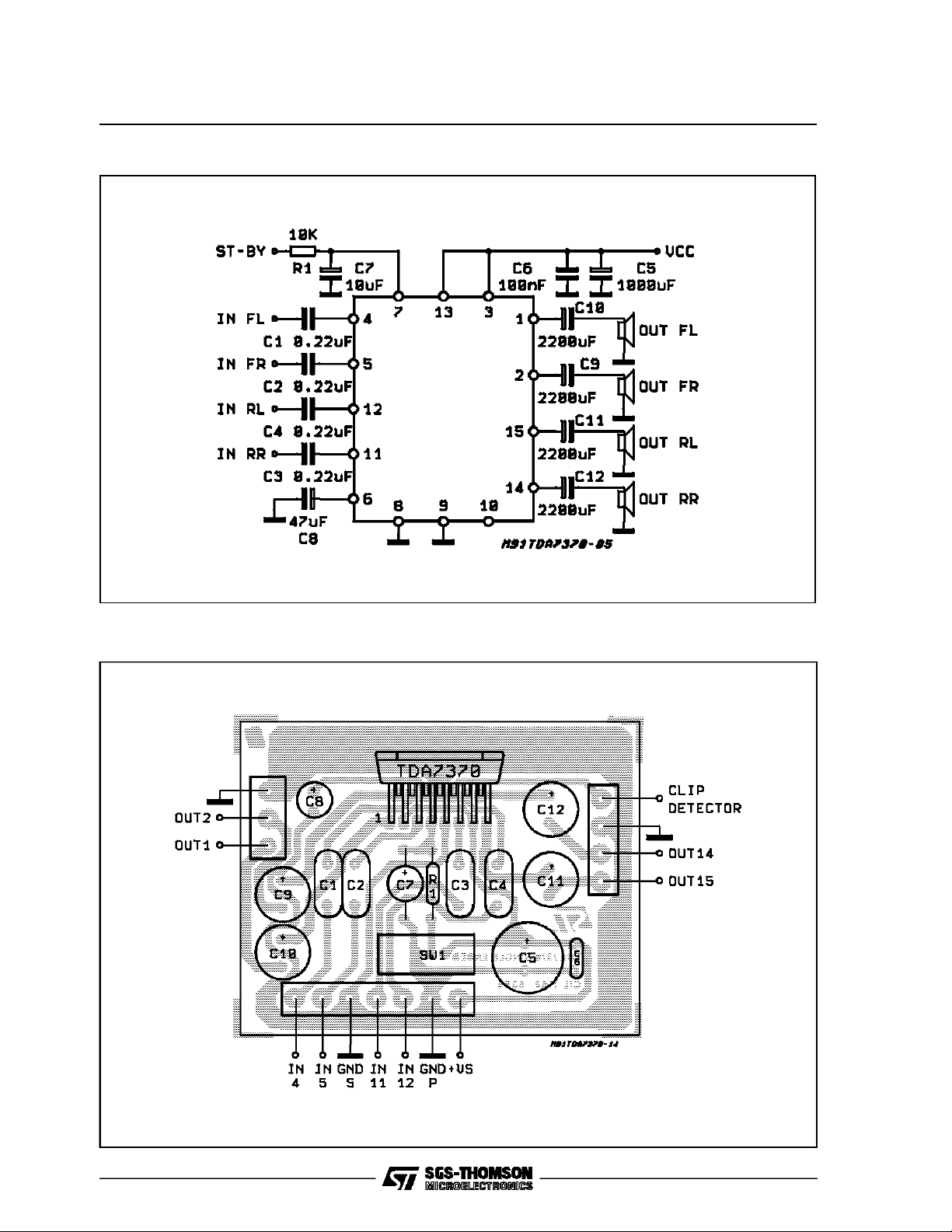
APPLICATIONCIRCUIT (QUADSTEREO)
QUAD STEREO P.C. BOARDAND COMPONENT LAYOUT(1:1 SCALE)
4/17
APPLICATIONCIRCUIT (DOUBLEBRIDGE)
TDA7370
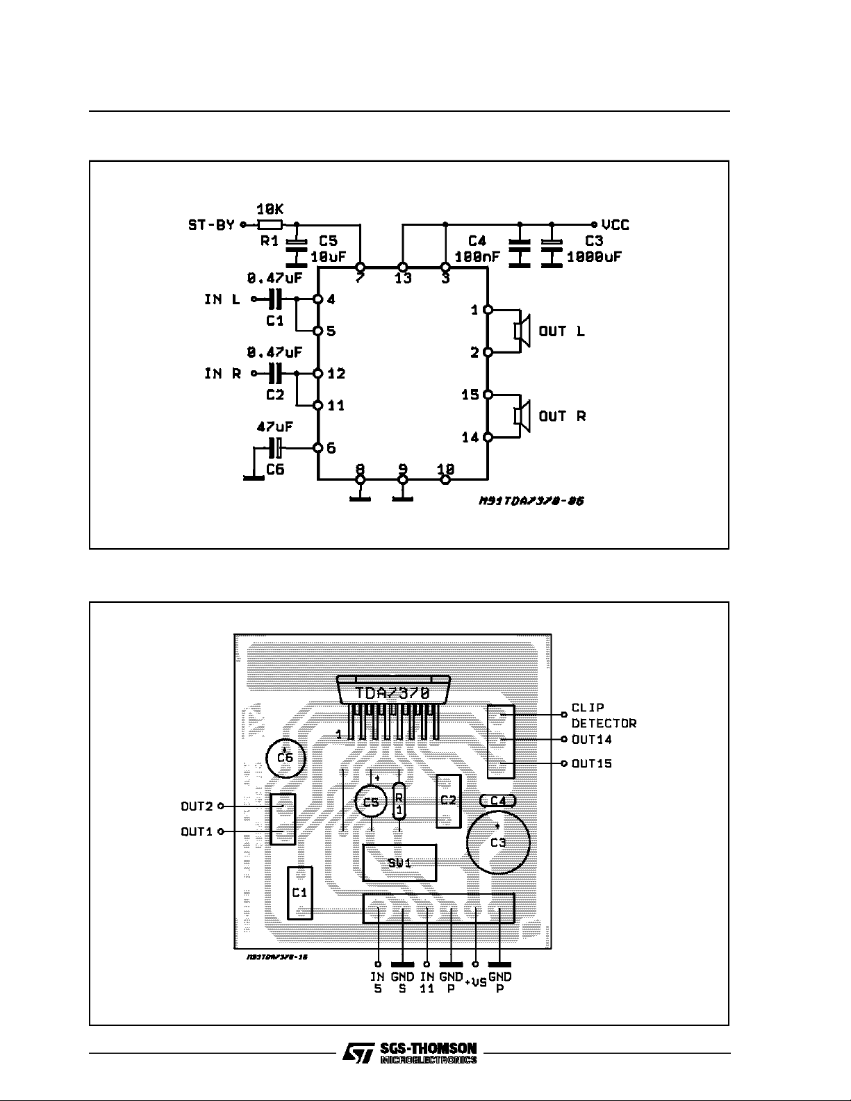
DOUBLE BRIDGEP.C. BOARD AND COMPONENTLAYOUT(1:1 SCALE)
5/17
TDA7370
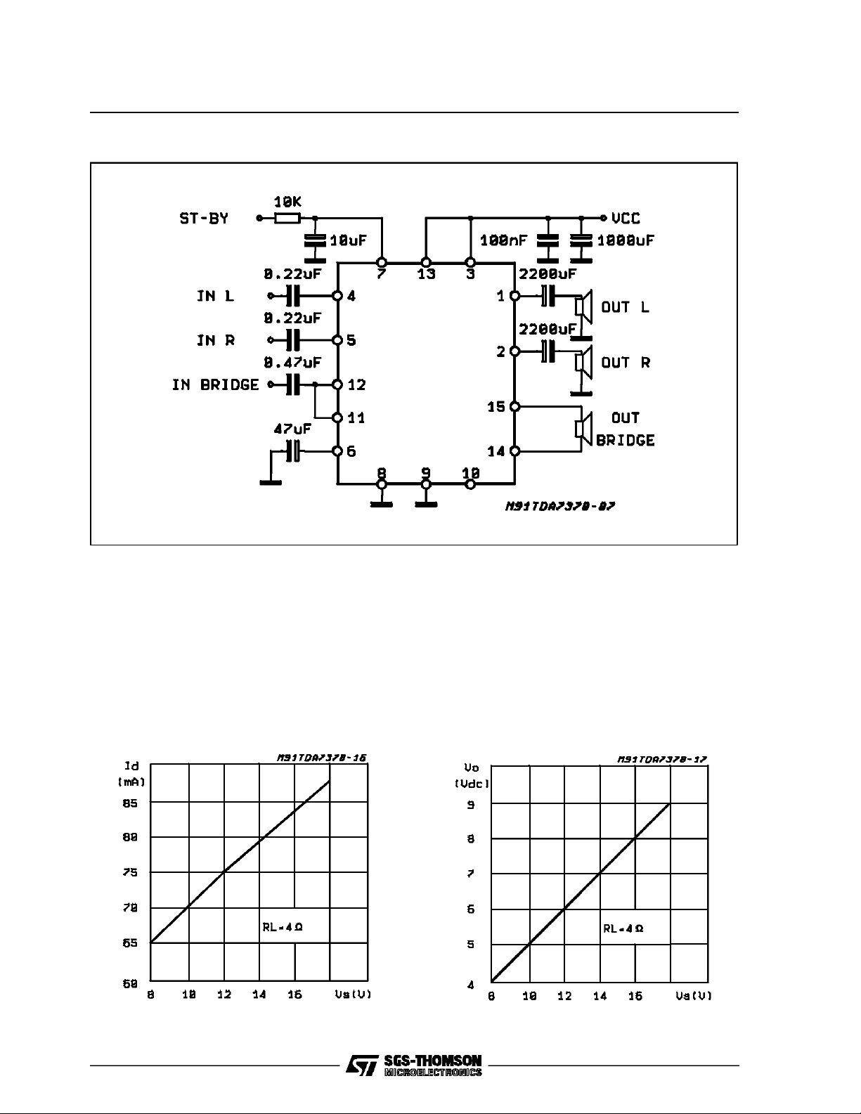
APPLICATIONCIRCUIT (STEREO/BRIDGE)
Figure1: QuiescentDrain Current vs. Supply
Voltage(Bridge/SingleEnded)
6/17
Figure2: QuiescentOutputVoltage vs. Supply
Voltage(Bridge/SingleEnded)

TDA7370
Figure3: Output Power vs. Supply Voltage
(SingleEnded)
Figure5: Distortion vs. OutputPower (Single
Ended)
Figure4: OutputPower vs. Supply Voltage
(Bridge)
Figure6: Distortionvs. Output Power (Bridge)
Figure7: Output Power vs. Frequency (Single
Ended)
Figure8: OutputPower vs. Frequency (Bridge)
7/17

TDA7370
Figure9: SupplyVoltage Rejection vs.
Frequency(SingleEnded)for different
valuesof pin 6 capacitor.
R
g
Figure10: SupplyVoltageRejection vs.
Frequency(Bridge)for different
values of pin 6 capacitor.
R
g
Figure11: Cross-Talkvs. Frequency(Bridge) Figure 12: Stand-ByAttenuation vs. Threshold
Voltage(SingleEnded/Bridge)
R
g
Figure13: ClippingDetector AverageCurrent
(pin 10) vs.Distortion(Single Ended)
Figure14: En input vs. R
(SingleEnded)
S
8/17

TDA7370
Figure15: En input vs. R
(SingleEnded)
S
Figure17: TotalPower Dissipation and
Efficiency vs. Ouput Power (Single
Ended)
Figure16: En input vs. R
R
g
(Bridge)
S
R
g
Figure18: TotalPower Dissipation and
Efficiencyvs.Ouput Power (Bridge)
9/17

TDA7370
OUTPUTSTAGE
The fully complementary output stage was made
possible by the development of a new component: the ST exclusive powerICV PNP.
A novel design based upon the connection shown
in fig. 19 has then allowed the full exploitation of
its possibilities.
Figure19: The new Output Stage
The clear advantages this new approachhas over
classicaloutput stages are as follows:
1 - Rail-to-Rail Output Voltage Swing With No
NeedOf BootstrapCapacitors.
The output swing is limited only by the Vcesat of
the output transistors, which are in the range of
0.6 Ohm (R
) each.
sat
Classical solutions adoptingcomposite PNP-NPN
for the upper output stage have higher saturation
loss on the top side of the waveform. This unbalanced saturation causes a significant power reduction. The only way to recover power consists
of the addition of expensivebootstrapcapacitors.
2 - Absolute Stability Without Any External
Compensation.
Referring to the circuit of Fig. 19 the gain
V
OUT/VIN
R2/R1.The DC output (V
is greater than unity, approximately 1 +
/2) is fixed by an aux-
CC
iliaryamplifiercommon to all the channels).
By controlling the amount of this local feedback it
is possible to force the loop gain (A * β) to less
than unity at frequency for which the phase shift
is 180 Deg. This means that the output buffer is
intrinsicallystable and not prone to oscillation.
Most remarkably, the above feature has been
achievedin spite of the very low closed loop gain
of the amplifier (20 dB).
In contrast, with the classical PNP-NPN stage,
the solution adopted for reducing the gain at high
frequencies makes use of external RC networks,
namelythe Boucherotcells.
OTHEROUTSTANDINGCHARACTERISTICS:
Clipping Detector Output
The TDA7370 is equipped with an internal circuit
able to detect the output stage saturation providing a current sinking into a open collector output
(pin 10) when a certain distortion level is reached
ateach output.
This particular function allows gain compression
facility whenever the amplifier is overdriven, thus
obtaininghigh quality sound at all listeninglevels.
Figure20: Clipping DetectionWaveforms
10/17

TDA7370
OffsetControl
The quiescent output voltage must be as close as
possible to its nominal value, so that less undistortedpower wouldbe available.
For this reason an input bias current compensation is implemented to reduce the voltage drop
across the input resistors, which appears amplified at the outputs.
Gain Internally Fixed to 20dB in Single Ended,
26dB in Bridge
Advantagesof this design choiceare in terms of:
componentsand space saving
output noise, supply voltage rejection and dis-
tortionoptimization.
Silent Turn On/Off and Muting/Stand-by Function
The stand-bycan be easily activated by means of
a CMOS level applied to pin 7 through a RC filter.
Under stand-by condition the device is turned off
completely(supply current= 1 µA TYP ; output attenuation=90 dB TYP).
Every ON/OFF operation is virtuallypop free.
Furthermore,at turn-on the device stays in muting
condition for a time determined by the value assigned to the SVR capacitor (T= Csvr
7,000).
*
While in muting the device outputs becomes insensitive to any kinds of signal that may be present at the input terminals. In other words every
transient coming from previous stages produces
no unpleasantacoustic effect to the speakers.
Anothersituation under which the device is totally
muted is whenever the supply voltage drops
lower than 7V. This is helpful to pop suppression
duringthe turn-off by battery switch.
BUILT-INPROTECTIONSYSTEMS
Full Protection of Device and Loudspeakers
Against AC/DC Short Circuits (to Gnd, to Vs,
across the Speakers).
Reliable and safe operation in presence of all
kinds of short circuit involving the outputs is assuredby a built-in protectionsystem that operates
in the following way:
In case of overload, a SCR is activated as soon
as the current flowing through the output transistors overcomes a preset threshold value depending on the chip temperature. The SCR causes an
interruption of the supply current of the power
transistor.The normal working is restoredby a restart circuit going into action as soon as the short
circuitis removed.
LoadDump Voltage Surge
The TDA 7370 has a circuit which enables it to
withstand a voltage pulse train on pins 3 and 13,
of the type shown in fig. 22.
If the supply voltage peaks to more than 50V,
then an LC filter must be inserted between the
supply and pins 3 and 13, in order to assure that
the pulses at pins 3 and 13 will be held within the
limitsshown.
A suggestedLC networkis shown in fig. 21.
With this network, a train of pulses with amplitude
up to 120V and width of 2ms can be applied at
point A. This type of protection is ON when the
supply voltage (pulse or DC) exceeds 18V. For
this reason the maximum operating supply voltage is 18V.
Figure21
EasySingle Ended to Bridge Transition.
The change from single ended to bridge configurations is made simply by means of a short circuit
across the inputs, that is no need of furtherexternal components.
High ApplicationFlexibility
The availability of 4 independentchannelsmakes
it possible to accomplishseveral kinds of applications ranging from 4 speakers stereo (F/R) to 2
speakersbridge solutions.
In case of working in single ended conditions the
polarity of the speakers driven by the inverting
amplifier must be reversed respect to those
drivenby non invertingchannels.
This is to avoid phase inconveniences causing
sound alterations especially during the reproduction of low frequencies.
Figure22
11/17

TDA7370
PolarityInversion
High current (up to 10A) can be handled by the
device with no damage for a longer period than
the blow-out time of a quick 2A fuse (normally
connected in series with the supply). This features is added to avoid destruction,if during fitting
to the car, a mistake on the connection of the
supplyis made.
Open Ground
When the radio is in the ON condition and the
ground is accidentally opened, a standard audio
amplifier will be damaged. On the TDA7370 protectiondiodes are includedto avoid any damage.
InductiveLoad
A protection diode is provided to allow use of the
TDA7370with inductiveloads.
DC Voltage
The maximum operating DC voltage for the
TDA7370is18V.
However the device can withstand a DC voltage
up to 28V with no damage. This could occur during winter if two batteries are series connected to
crankthe engine.
safety compared with that of a conventional
circuit. There is no device damage in case of
excessive junction temperature: all happens
is that P
(and therefore P
o
) and Idare re-
tot
duced.
The maximum allowable power dissipation depends upon the size of the external heatsink (i.e.
its thermal resistance); Fig. 23 shows the dissipablepower as a function of ambienttemperature
for different thermal resistance.
Figure23: MaximumAllowablePower
Dissipationvs. AmbientTemperature
ThermalShut-down
The presence of a thermal limiting circuit offers
the following advantages:
1)an overload on the output (even if it is permanent), or an excessive ambient temperature
can be easily withstood.
2)the heatsink can have a smaller factor of
Loudspeaker Protection
TheTDA7370 guaranteessafe operationseven for
theloudspeakerin caseof accidentalshortcircuit.
Whenevera single OUT to GND, OUT to V
S
short
circuit occurs both the outputs are switched OFF
so limiting dangerous DC current flowing through
the loudspeaker.
12/17

TDA7370
CLIPPINGDETECTOR
Figures 25 and 26 show an application using the
TDA7370 in combination with the SGS-THOMSONaudioprocessorTDA7302.
The output clipping is recognized by the microprocessor (in this application it is simulated by a
PC).
The detailed way to operate of the system is representedby the flow-chartof fig.24
The controller detects when the clipping is active
(minimun detection width fixed by a C29 = 12 nF
external capacitor), and reduces the volume (or
bass ) by steps of 2 dB (with a programmable
waiting time), until no more clippingis detected.
Then the controller waits for a programmabletime
before increasing the volume again by step of 2
dBuntil clippingis again detected or the panelselectedvolume is reached.
Practicaladvantages of this applicationis a better
sound quality deriving from operation under no
clipping conditions, which also means the avail-
Figure24: Clipping DetectorControl Routine
abilityof higherundistortedpower.
WHAT IS NEEDED FOR A DEMONSTRATION
- a XT or AT IBM compatible PC, supplied with
EGA card
- a SGS-THOMSONaudioprocessorapplicationdisk
- a TDA 7302 + TDA7370board
- a connector from audioprocessor board to PC
parallelport
GENERALINFORMATION
In the application shown in figures 25 and 26 the
TDA7302 audioprocessorworks on PC XT or AT
IBM compatible.
Control is accomplished by serial bus ( S-bus or
2
C-bus or SPI bus)sent to the test board through
I
the PC parallel port.
ThePC simulatesthe behaviourof the microprocessor in a real application (for example in a car
radio) and the buffer is necessary only in this applicationfor protectingthe PC.
13/17

TDA7370
Figure25: Applicationwith TDA7302+ TDA7370 (QUADSTEREO)
14/17

Figure26: Applicationwiyh TDA7302+ TDA7370 (DOUBLE BRIDGE)
TDA7370
15/17

TDA7370
MULTIWATT15 PACKAGE MECHANICAL DATA
DIM.
MIN. TYP. MAX. MIN. TYP. MAX.
A 5 0.197
B 2.65 0.104
C 1.6 0.063
D 1 0.039
E 0.49 0.55 0.019 0.022
F 0.66 0.75 0.026 0.030
G 1.14 1.27 1.4 0.045 0.050 0.055
G1 17.57 17.78 17.91 0.692 0.700 0.705
H1 19.6 0.772
H2 20.2 0.795
L 22.1 22.6 0.870 0.890
L1 22 22.5 0.866 0.886
L2 17.65 18.1 0.695 0.713
L3 17.25 17.5 17.75 0.679 0.689 0.699
L4 10.3 10.7 10.9 0.406 0.421 0.429
L7 2.65 2.9 0.104 0.114
M 4.2 4.3 4.6 0.165 0.169 0.181
M1 4.5 5.08 5.3 0.177 0.200 0.209
S 1.9 2.6 0.075 0.102
S1 1.9 2.6 0.075 0.102
Dia1 3.65 3.85 0.144 0.152
mm inch
16/17

TDA7370
Information furnished is believed to be accurate and reliable. However,SGS-THOMSON Microelectronics assumes no responsibility for the
consequences of use of such information nor for any infringement of patents or other rights of third parties which may result from its use. No
license is granted by implication or otherwise under any patent or patent rights of SGS-THOMSON Microelectronics. Specifications mentioned in this publication are subject to change without notice. This publication supersedes and replaces all information previously supplied.
SGS-THOMSON Microelectronics products are not authorized for use as critical components in life support devices or systems without express written approval of SGS-THOMSON Microelectronics.
1995 SGS-THOMSON Microelectronics - All RightsReserved
MULTIWATTis a Registered Trademark of the SGS-THOMSON Microelectronics
SGS-THOMSON Microelectronics GROUPOF COMPANIES
Australia - Brazil - France -Germany - Hong Kong - Italy - Japan - Korea - Malaysia - Malta - Morocco - The Netherlands - Singapore -
Spain - Sweden - Switzerland - Taiwan - Thaliand - United Kingdom - U.S.A.
17/17
 Loading...