OUTPUT POWER 2x6W/4Ω @14.4V, 1KHz,
10%
SOLIDSTATEPOWERSWITCH INCLUDED
(1A @ V
MINIMUMEXTERNALCOMPONENTCOUNT
- INTERNALLY FIXED GAIN (40dB)
- NO BOOTSTRAPCAPACITORS
- NO EXTERNALCOMPENSATION
ST-BYFUNCTION(CMOS COMPATIBLE)
MUTE FUNCTION (CMOS COMPATIBLE)
NO AUDIBLE POP DURING MUTE/ST-BY
OPERATIONS
LOW SUPPLY SELFMUTING
PROTECTIONS
AC AUDIO OUTPUTS SHORT CIRCUIT TO
GND
DC AUDIO OUTPUTS SHORT CIRCUIT TO
GNDAND TOV
SWITCH OUTPUT INTERNAL CURRENT
LIMITATION
OVERRATING CHIP TEMPERATURE WITH
SOFT THERMAL LIMITER
LOADDUMP
FORTUITOUS OPENGND
DROP
= 0.8V Typ.)
AT POWER ON
S
TDA7365
2 x 6W CAR RADIO AMPLIFIER
PLUS SOLID STATE SWITCH
ADVANCE DATA
MULTIWATT15
ORDERING NUMBER: TDA7365
REVERSEBATTERY
ESD
DESCRIPTION
TheTDA7365is a newtechnologyDual Audio Amplifier in Multiwatt15 package especially designed
forstereo car radio applications.
Thanksto the fully complementaryoutput configuration the TDA7365 delivers a rail to rail voltage
swingwith no needof boostrapcapacitors
It includesa solidstateswitch,enabledby a ST-BY
function common to the audio section, suitable for
supplyingboth the signalprocessingpart of the car
radioset and the lamps. As a resultsthe power-on
operation is simplified, thereby saving cost and
space inthewhole powersection.
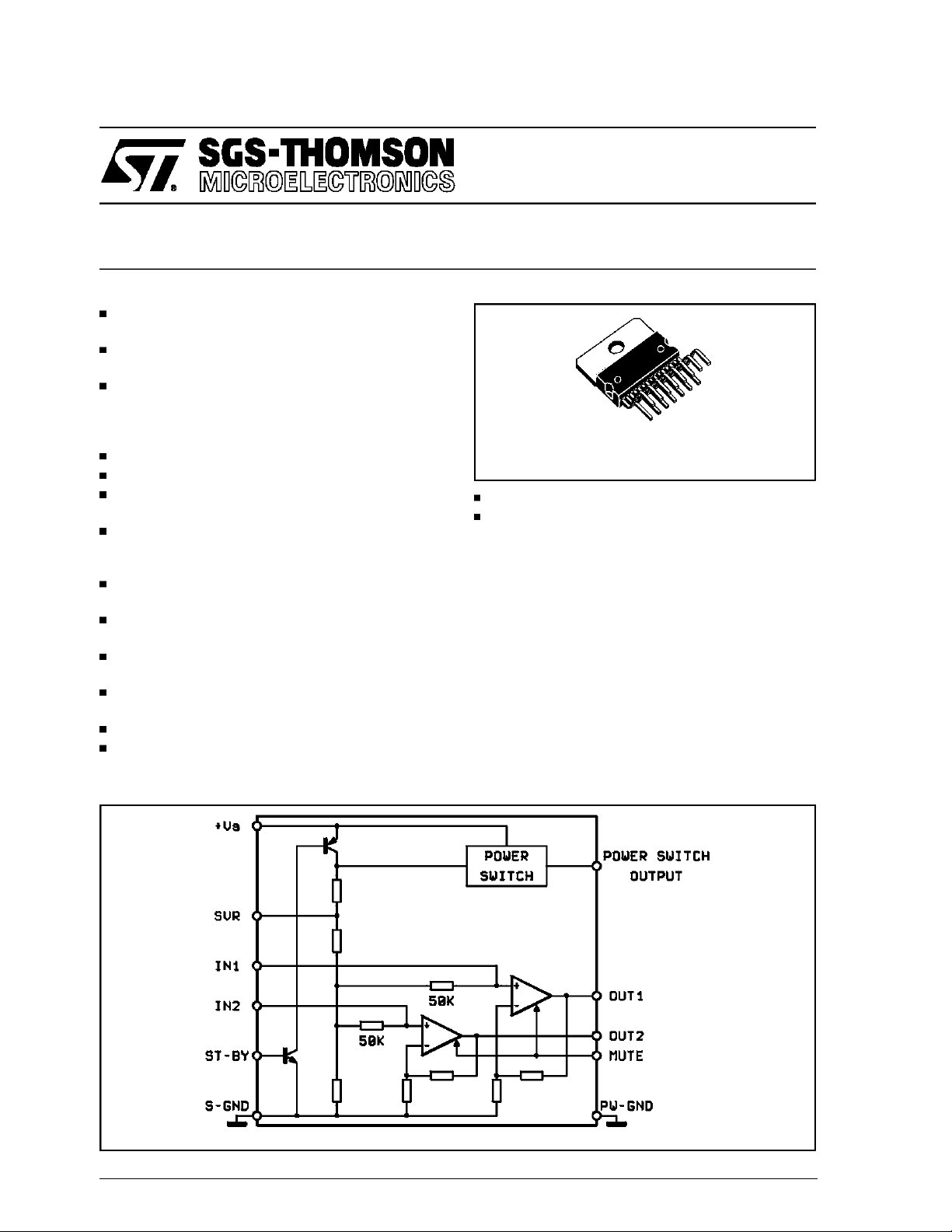
BLOCK DIAGRAM
April 1995
This isadvanced information on a new product now in development or undergoing evaluation.Details are subject to change without notice.
1/7

TDA7365
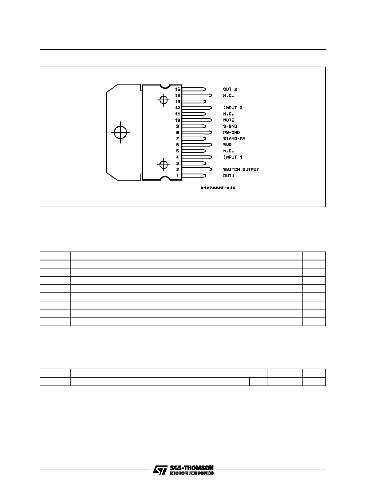
PIN CONNECTION (Top view)
Vs
Vs
ABSOLUTE MAXIMUM RATINGS
Symbol Parameter Value Unit
V
V
V
PEAK
P
T
stg,Tj
I
I
I
DC Supply Voltage 28 V
S
Operating Supply Voltage 18 V
OP
Peak Supply Voltage (t = 50ms) 40 V
Audio Channels Output Peak Current (notrep. t = 100µs) 4 A
O
Audio Channels Output Peak Current (rep.f > 10Hz) 3 A
O
Switch OutputPeak Current (internally limited) 1.5 A
O
Power Dissipation (T
tot
=85°C) 32 W
case
Storage and JunctionTemperature -40 to 150 °C
THERMAL DATA
Symbol Description Value Unit
R
th j-case
Thermal Resistance Junction-case Max 2 °C/W
2/7

TDA7365
ELECTRICAL CHARACTERISTICS (Referto the test circuit; VS=14.4V; RL=4Ω,T
amb
=25°C,
f = 1kHz, unlessotherwise specified)
Symbol Parameter Test Condition Min. Typ. Max. Unit
V
S
I
d
P
O
Supply Range 8 18 V
Total Quiescent Drain Current Power Switch Unloaded 80 mA
Output Power RL=4Ω; THD =10%
5.5 6 W
each channel
R
=2Ω; THD =10%
L
9W
each channel
d Distortion P
CT Cross Talk f = 1kHz; R
R
IN
G
V
G
V
E
IN
Input Impedance 40 50 KΩ
Voltage Gain 39 40 41 dB
Voltage Gain Match. 1 dB
Input Noise Voltage (*) Rg= 0 1.2 5 µV
SVR Supply Voltage Rejection R
= 0.1 to 3W 0.08 0.3 %
O
f = 10kHz; R
= 0 ; f = 100Hz;
g
V
= 0.5V
r
rms
g
=0
=0
g
50 55
50
45 50 dB
ASB Stand-by Attenuation 60 90 dB
V
V
SB OUT
V
V
MOUT
I
SB
SB IN
MIN
ST-BY Current Consumption 100 µA
ST-BY IN Threshold Voltage 1.5 V
ST-BY OUT Threshold Voltage 3.5 V
MUTE IN Threshold Voltage 1.5 V
MUTE OUT Threshold Voltage 3.5 V
POWERSWITCH CHARACTERISTICS
dB
dB
Symbol Parameter Test Condition Min. Typ. Max. Unit
I
Op
V
DROP
(*) 22Hz to 22KHz
(**) A weighted
Continuous Output Current 1.2 A
Dropout Voltage Io = 1A 1.4 V
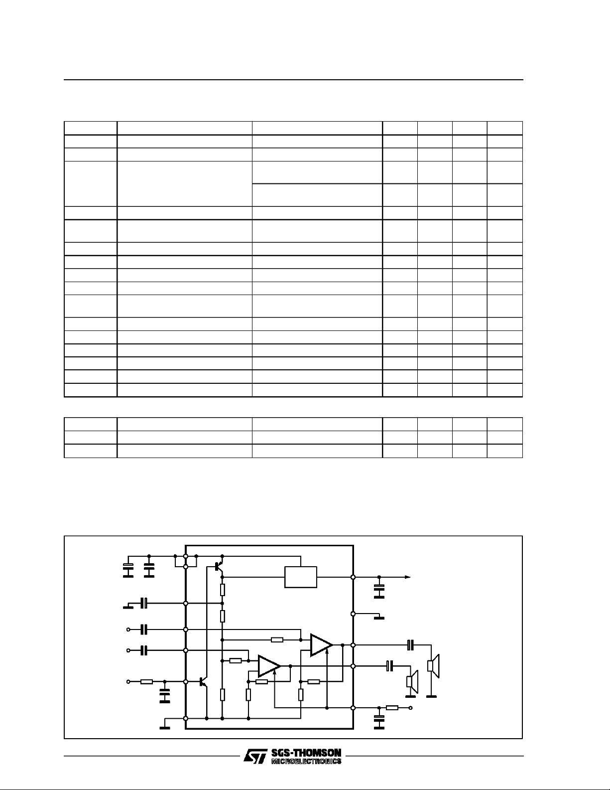
TEST AND APPLICATION CIRCUIT
+V
s
470µF
C5
47µF C10
0.22µFC1
0.22µFC2
10K R1
0.1µF
C7
0.1µF
C6
ST-BY
S-GND
SVR
IN1
IN2
50K
50K
POWER
SWITCH
PWR SWITCH
OUTPUT
4.7µF
PW-GND
OUT1
1000µFC4
OUT2
10K R2
MUTE
10µF
VOLTAGE REGULATOR
SUPPLYING THE LOW
C9
C8
SIGNAL SECTION
1000µFC3
D94AU116B
TO THE
3/7

TDA7365
Figure1: P.C.Boardand component layoutof theTest and ApplicationCircuit1:1 scale.
Figure 2: Quiescent Drain Current vs. Supply
Figure3: OutputPower vs. Supply Voltage
Voltage
Figure4: OutputPower vs. Supply Voltage Figure5: Distortion vs. Output Power
4/7

TDA7365
Fiigure6: Distortion vs. Frequency
Fiigure 8: Cross-Talkvs. Frequency
Figure7: SupplyVoltage Rejection
Figure9: Switch Drop-out vs. Switch Current
Figure 10: TotalPower Dissipation and Efficiency
vs. Output Power
Figure11: TotalPower Dissipation and Efficiency
P
(W)
tot
P
tot
5/7

TDA7365
MULTIWATT15 PACKAGEMECHANICAL DATA
DIM.
MIN. TYP. MAX. MIN. TYP. MAX.
A 5 0.197
B 2.65 0.104
C 1.6 0.063
D 1 0.039
E 0.49 0.55 0.019 0.022
F 0.66 0.75 0.026 0.030
G 1.14 1.27 1.4 0.045 0.050 0.055
G1 17.57 17.78 17.91 0.692 0.700 0.705
H1 19.6 0.772
H2 20.2 0.795
L 22.1 22.6 0.870 0.890
L1 22 22.5 0.866 0.886
L2 17.65 18.1 0.695 0.713
L3 17.25 17.5 17.75 0.679 0.689 0.699
L4 10.3 10.7 10.9 0.406 0.421 0.429
L7 2.65 2.9 0.104 0.114
M 4.2 4.3 4.6 0.165 0.169 0.181
M1 4.5 5.08 5.3 0.177 0.200 0.209
S 1.9 2.6 0.075 0.102
S1 1.9 2.6 0.075 0.102
Dia1 3.65 3.85 0.144 0.152
mm inch
6/7

TDA7365
Information furnished is believed to be accurate and reliable. However, SGS-THOMSON Microelectronics assumes no responsibility for the
consequences of use of such informationnor for any infringement of patents or other rights of third parties which may result from itsuse. No
license is granted by implication or otherwise under any patent or patent rights of SGS-THOMSON Microelectronics. Specifications mentioned in thispublication are subject to change withoutnotice. This publication supersedes and replaces all informationpreviously supplied.
SGS-THOMSON Microelectronics products are not authorized for use as critical components in life support devices or systems withoutexpress written approval of SGS-THOMSON Microelectronics.
1995 SGS-THOMSON Microelectronics - All RightsReserved
MULTIWATT is Registered Trademark of SGS-THOMSON Microelectronics
SGS-THOMSON Microelectronics GROUP OF COMPANIES
Australia - Brazil - France - Germany - Hong Kong - Italy - Japan - Korea - Malaysia -Malta - Morocco - The Netherlands- Singapore-
Spain - Sweden - Switzerland - Taiwan - Thaliand - United Kingdom - U.S.A.
7/7
 Loading...