


22W BRIDGE-STEREO AMPLIFIER FOR CAR RADIO
VERYFEW EXTERNALCOMPONENTS
NO BOUCHEROTCELLS
NO BOOSTRAPCAPACITORS
HIGHOUTPUT POWER
NO SWITCH ON/OFF NOISE
VERYLOW STAND-BYCURRENT
FIXED GAIN (30dB STEREO)
PROGRAMMABLETURN-ON DELAY
Protections:
OUTPUT AC-DC SHORT CIRCUIT TO
GROUNDANDTO SUPPLYVOLTAGE
VERYINDUCTIVE LOADS
LOUDSPEAKERPROTECTION
OVERRATINGCHIP TEMPERATURE
LOADDUMP VOLTAGE
FORTUITOUS OPEN GROUND
ESD
DESCRIPTION
The TDA7350A is a new technology class AB
Audio Power Amplifier in the Multiwatt
package
TDA7350A
MULTIWATT11
ORDERING NUMBER: TDA7350A
designedfor car radioapplications.
Thanks to the fully complementaryPNP/NPN output configuration the high power performance of
the TDA7350A is obtained without bootstrap capacitors.
A delayed turn-on mute circuit eliminates audible
on/off noise, and a novel short circuit protection
system prevents spurious intervention with highly
inductiveloads.
APPLICATIONCIRCUIT BRIDGE
April 1995
1/22
TDA7350A
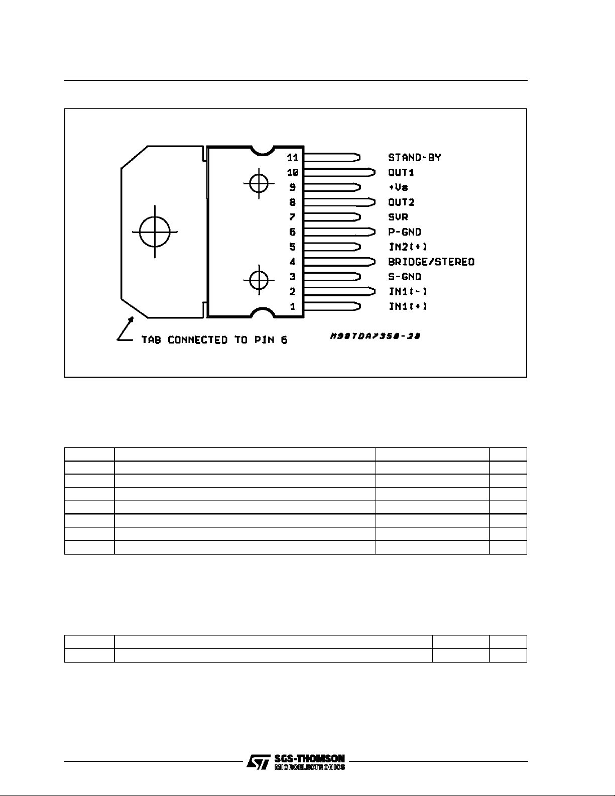
PIN CONNECTION (Top view)
ABSOLUTE MAXIMUMRATINGS
Symbol Parameter Test Conditions Unit
V
V
V
P
T
stg,TJ
Operating Supply Voltage 18 V
S
DC Supply Voltage 28 V
S
Peak Supply Voltage (for t = 50ms) 40 V
S
Output Peak Current (nonrep. for t = 100µs) 5 A
I
o
Output Peak Current (rep.freq. > 10Hz) 4 A
I
o
Power Dissipation at T
tot
=85°C36W
case
Storage and Junction Temperature -40 to 150 °C
THERMAL DATA
Symbol Description Value Unit
R
thj-case
Thermal Resistance Junction-case Max 1.8 °C/W
2/22
TDA7350A
ELECTRICAL CHARACTERISTICS (Referto the test circuits, T
=25°C, VS=14.4V, f = 1KHz unless
amb
otherwisespecified)
Symbol Parameter Test Condition Min. Typ. Max. Unit
V
I
A
I
SB
T
Supply Voltage Range 8 18 V
S
Total Quiescent Drain Current stereo configuration 120 mA
d
Stand-by attenuation 60 80 dB
SB
Stand-by Current 100 µA
Thermal Shut-down Junction
sd
150 °C
Temperature
STEREO
P
d Distortion P
SVR Supply Voltage Rejection R
CT Crosstalk f = 1KHz
R
G
G
E
Output Power (each channel) d = 10%
o
R
=2Ω
L
R
= 3.2Ω
L
R
=4Ω
L
d = 10%; V
R
=2Ω
L
R
= 3.2Ω
L
R
=4Ω
L
= 0.1 to 4W; RL= 3.2Ω 0.5 %
o
= 10kΩ C3 = 22µF
g
= 13.2V
S
7
45 50
f = 100Hz C3 = 100µF
11
8
6.5
9
6.5
5.5
57
45 55
f = 10KHz
Input Resistance 30 50 KΩ
I
Voltage Gain 27 29 31 dB
V
Voltage Gain Match 1 dB
V
Input Noise Voltage Rg=50Ω(*)
IN
R
= 10KΩ (*)
g
R
Ω(**)
g=50
R
= 10KΩ (**)
g
50
1.5
2
2
2.7 7
BRIDGE
W
W
W
W
W
W
dB
dB
dB
µV
µV
µV
µV
P
Output Power d = 10%; RL=4Ω
o
d Distortion P
V
Output Offset Voltage 250 mV
OS
SVR Supply Voltage Rejection R
R
G
E
(*) Curve A
(**) 22Hz to 22KHz
Input Resistance 50 KΩ
I
Voltage Gain 33 35 37 dB
V
Input Noise Voltage Rg=50Ω(*)
IN
d = 10%; R
d = 10%; V
R
=4Ω
L
R
= 3.2Ω
L
= 0.1 to 10W; RL=4Ω 1%
o
= 10KΩ C3 = 22µF
g
f = 100Hz C3 = 100µF
= 3.2Ω
L
= 13.2V
S
16
22
17.5
19
45 50
57
2
20
R
g = 10K
R
=50Ω(**)
g
R
= 10KΩ (**)
g
Ω (*)
2.5
2.7
3.2
W
W
W
W
dB
µV
µV
µV
µV
3/22
TDA7350A
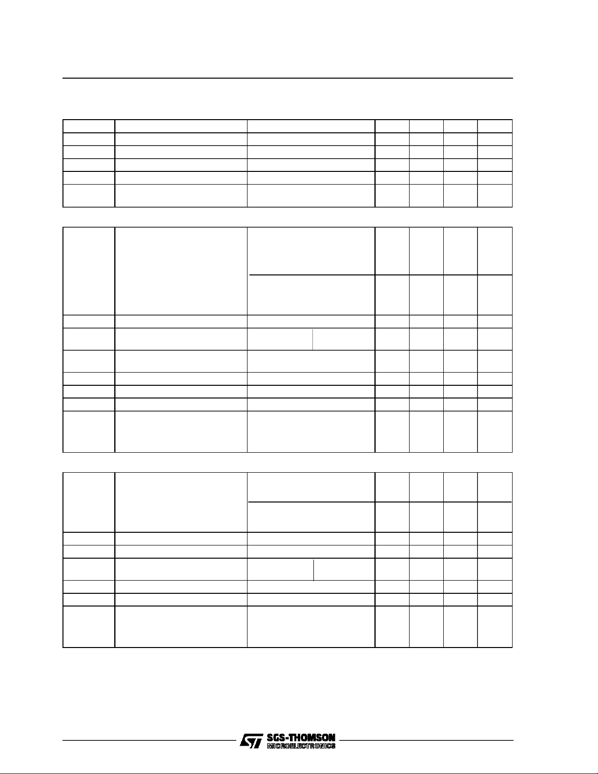
Figure1: STEREO Test and Appication Circuit
220µF
220µF
Figure2: P.C. Boardand Layout(STEREO) ofthe circuitof fig. 1 (1:1 scale)
1000µF
1000µF
4/22
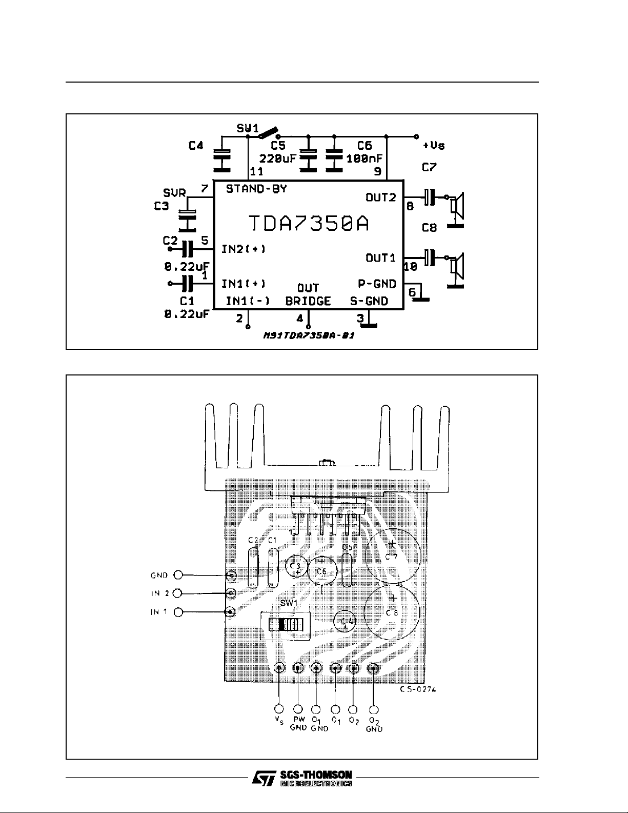
Figure3: BRIDGE Test and AppicationCircuit
Figure4: P.C. Boardand Layout(BRIDGE) of the circuitof fig. 3 (1:1scale)
TDA7350A
5/22
TDA7350A
RECOMMENDED VALUES OF THE EXTERNAL COMPONENTS (ref to the Stereo Test and Applica-
tionCircuit)
Component
C1 0.22µF Input
C2 0.22µF Input
C3 100µF Supply Voltage
C4 22µF Stand-By
C5 220µF (min) SupplyBy-Pass Dangerof Oscillations
C6 100nF (min) SupplyBy-Pass Dangerof Oscillations
C7 2200µF Output
Recommended
Value
Purpose
Decoupling
(CH1)
Decoupling
(CH2)
Rejection
Filtering
Capacitor
ON/OFF Delay
Decoupling
CH2
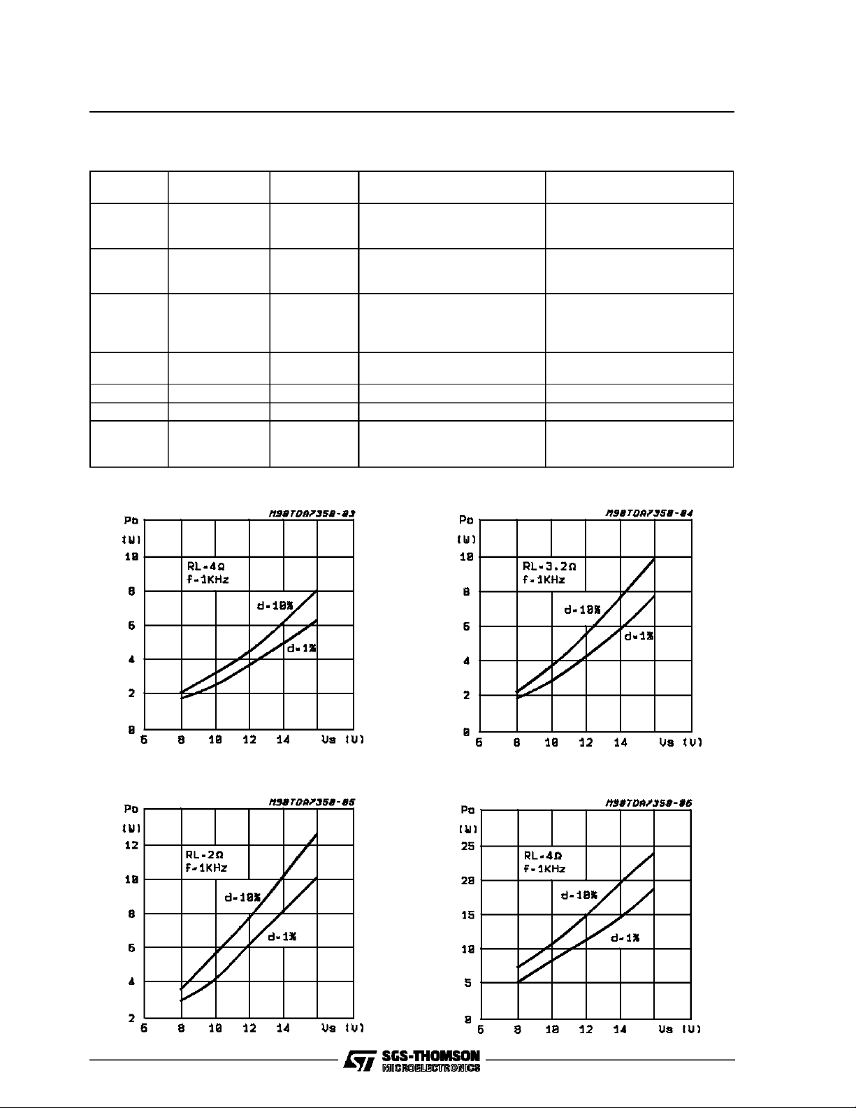
Figure5: OutputPowervs. SupplyVoltage
(Stereo)
Larger than the Recomm.
Value
——
——
Longer Turn-On Delay Time Worse Supply Voltage Rejection.
Delayed Turn-Offby Stand-By
Switch
- Decrease ofLow Frequency Cut Off
- Longer Turn On Delay
Smaller than the Recomm.
Shorter Turn-On Delay Time
Dangerof Noise (POP)
Dangerof Noise (POP)
- Increase of Low Frequency Cut Off
- Shorter Turn On Delay
Figure6: OutputPowervs. SupplyVoltage
(Stereo)
Value
Figure7: OutputPowervs. SupplyVoltage
(Stereo)
6/22
Figure8: OutputPowervs. SupplyVoltage
(Bridge)
TDA7350A
Figure9: Output Powervs. SupplyVoltage
(Bridge)
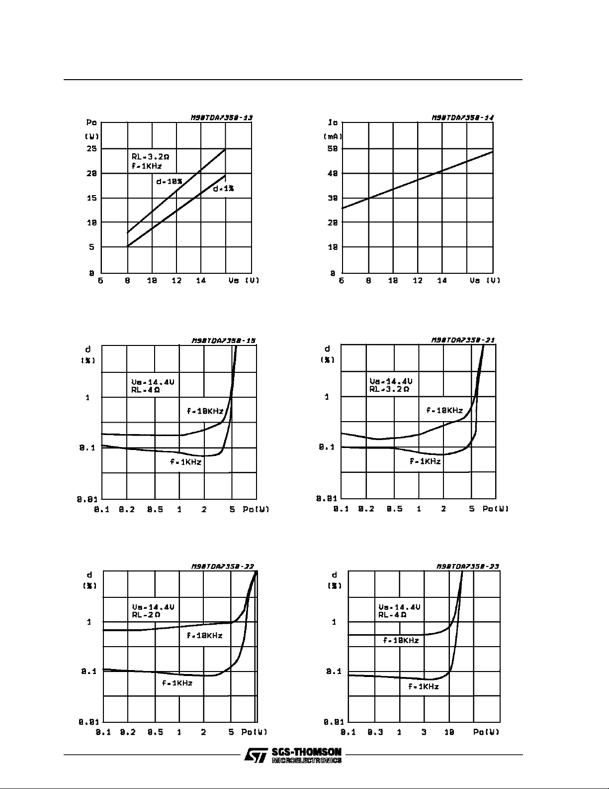
Figure 11: Distortionvs OutputPower(Stereo)
Figure 10: Drain Current vs SupplyVoltage
(Stereo)
Figure 12: Distortionvs OutputPower(Stereo)
Figure 13: Distortionvs OutputPower(Stereo) Figure14: Distortion vs OutputPower(Bridge)
7/22

TDA7350A
Figure15: SVR vs. Frequency& C
R
g
Figure17: SVR vs. Frequency& C
(Stereo) Figure16: SVR vs. Frequency& C
SVR
; (Bridge) Figure 18: SVR vs. Frequency & C
SVR
; (Stereo)
SVR
R
g
; (Bridge)
SVR
R
g
R
g
Figure19: Crosstalk vs. Frequency(Stereo) Figure20: PowerDissipation & Efficiencyvs.
OutputPower(Stereo)
8/22
R
g

TDA7350A
Figure21: PowerDissipation& Efficiencyvs.
OutputPower(Stereo)
Figure22: Power Dissipation& Efficiencyvs.
OutputPower(Bridge)
saving due to the minimized external count, excellent electrical performances, flexibility in use,
superiorreliability thanks to a built-inarray of protections. As a result the following performances
hasbeen achieved:
NO NEED OF BOOTSTRAP CAPACITORS
EVEN AT THE HIGHEST OUTPUT POWER
LEVELS
ABSOLUTE STABILITY WITHOUT EXTERNAL COMPENSATION THANKS TO THE INNOVATIVE OUT STAGE CONFIGURATION,
ALSO ALLOWING INTERNALLY FIXED
CLOSED LOOP LOWER THAN COMPETITORS
LOW GAIN (30dB STEREO FIXED WITHOUT
ANY EXTERNAL COMPONENTS) IN ORDER
TO MINIMIZE THE OUTPUT NOISE AND OPTIMIZESVR
SILENT MUTE/ST-BY FUNCTION FEATURING ABSENCEOF POP ON/OFF NOISE
HIGHSVR
STEREO/BRIDGE OPERATION WITHOUT
ADDITIONOF EXTERNAL COMPONENT
AC/DC SHORT CIRCUIT PROTECTION (TO
GND,TO V
, ACROSSTHE LOAD)
S
LOUDSPEAKERPROTECTION
DUMP PROTECTION
ESDPROTECTION
Figure23: PowerDissipation & Efficiencyvs.
OutputPower(Bridge)
AMPLIFIER ORGANIZATION
The TDA7350A has been developed taking care
of the key concepts of the modern power audio
amplifier for car radio such as: space and costs
BLOCKDESCRIPTION
Polarization
The device is organized with the gainresistors directly connected to thesignal ground pin i.e.withoutgain capacitors(fig. 24).
The non inverting inputsof the amplifiers are connected to the SVR pin by means of resistor dividers, equal to the feedback networks. This allows
the outputs to track the SVR pin which is sufficiently slow to avoid audible turn-on and turn-off
transients.
SVR
The voltage ripple on the outputs is equal to the
one on SVR pin: with appropriate selection of
, more than 55dB of ripple rejection can be
C
SVR
obtained.
DelayedTurn-on (muting)
TheC
sets a signal turn-on delay too. A circuit
SVR
is included which mutes the device until the voltage on SVR pin reaches ~2.5V typ (fig. 25). The
mute function is obtained by duplicating the input
differential pair (fig. 26): it can be switched to the
signal source or to an internal mute input. This
feature is necessary to prevent transients at the
inputs reaching the loudspeaker(s) immediately
9/22

TDA7350A
afterpower-on).
Fig. 25 represents the detailed turn-on transient
with reference to the stereo configuration.
At the power-onthe output decoupling capacitors
are charged through an internal path but the device itself remains switched off (Phase 1 of the
representeddiagram).
When the outputsreach thevoltage level of about
1V (this means that there is no presence of short
circuits) the device switches on, the SVR capacitor starts charging itself and the output tracks exactly the SVR pin.
During this phase the device is muted until the
SVRreaches the ”Play” threshold(~2.5V typ.), after that the musicsignalstartsbeing played.
Stereo/Bridge Switching
Thereis also no need for externalcomponentsfor
Figure24: BlockDiagram; Stereo Configuration
changingfrom stereo to bridge configuration(figg.
24-27).
A simple short circuit between two pins allows
phase reversal at one output, yet maintaining the
quiescentoutput voltage.
Stand-by
The device is also equipped with a stand-byfunction, so that a low current, and hence low cost
switch,can be used forturn on/off.
Stability
The device is provided with an internal compensation wich allows to reach low values of closed
loop gain.
In this way better performances on S/N ratio and
SVRcan be obtained.
10/22

Figure25: Turn-onDelayCircuit
TDA7350A
11/22

TDA7350A
Figure26: MuteFunctionDiagram
Figure27: BlockDiagram; Bridge Configuration
12/22

TDA7350A
Figure28: ICV- PNP Gainvs. I
Figure29: ICV- PNP V
CE(sat
) vs. I
C
OUTPUT STAGE
Poor current capability and low cutoff frequency
are well known limits of the standardlateral PNP.
Composite PNP-NPN power output stages have
beenwidely used, regardlesstheir high saturation
drop. This drop can be overcome only at the expense of external components,namely, the bootstrap capacitors. The availability of 4A isolated
collector PNP (ICV PNP) adds versatility to the
design. The performance of this component, in
terms of gain, V
and cut-off frequency, is
CEsat
shown in fig. 28, 29, 30 respectively.It is realized
in a new bipolar technology, characterizedby topbottom isolation techniques, allowing the implementation of low leakage diodes, too. It guarantees BV
> 20V and BV
CEO
> 50V both for
CBO
NPN and PNP transistors. Basically, the connection shown in fig. 31 has been chosen. First of all
because its voltage swing is rail-to-rail, limited
only by the VCEsat of the output transistors,
which are in the range of 0.3Ω each. Then, the
C
gain VOUT/VIN is greater than unity, approximately 1+R2/R1. (VCC/2 is fixed by an auxiliary
amplifier common to both channel). It is possible,
controlling the amount of this local feedback, to
force the loop gain(A . β) to less than unity at frequencies for which the phase shift is 180°. This
means that the output buffer is intrinsically stable
and not prone to oscillation.
Figure30: ICV- PNP cut-off frequencyvs. I
Figure31: TheNew Output Stage
C
In contrast, with the circuit of fig. 32, the solution
adopted to reduce the gain at high frequenciesis
the use of an externalRC network.
AMPLIFIER BLOCK DIAGRAM
The block diagram of each voltage amplifier is
shown in fig. 33. Regardless of production
spread,the currentin each final stage is kept low,
with enough margin on the minimum,below which
cross-over distortion would appear.
13/22

TDA7350A
Figure32: A ClassicalOutput Stage
Figure33: AmplifierBlock Diagram
BUILT-INPROTECTIONSYSTEMS
Short CircuitProtection
The maximum current the device can deliver can
be calculated by considering the voltagethat may
be presentat the terminals of a carradio amplifier
and the minimum load impedance.
Apart from consideration concerning the area of
the power transistors it is not difficult to achieve
peak currents of this magnitude(5A peak).
However, it becomesmore complicated if AC and
DC short circuit protection is also required.In particular,with a protection circuit which limits the
output current following the SOA curve of the output transistors it is possible that in some conditions (highly reactive loads, for example) the protection circuit may intervene during normal
operation. For this reason each amplifier has
been equippedwith a protection circuit that interveneswhen the output current exceeds 4A.
Fig 34 shows the protection circuit for an NPN
power transistor (a symmetrical circuit applies to
PNP).The VBE of the power is monitored and
givesout a signal,availablethrough a cascode.
This cascode is used to avoid the intervention of
the short circuit protection when the saturation is
14/22
belowa givenlimit.
Thesignal sets a flip-flop whichforcesthe amplifier
outputsinto a highimpedancestate.
In case of DC short circuit when the short circuit
is removed the flip-flop is reset and restarts the
circuit (fig. 38). In case of AC short circuit or load
shorted in Bridge configuration,the device is continuously switched in ON/OFF conditions and the
currentis limited.
Figure34: Circuitry for Short Circuit Detection

TDA7350A
Load Dump Voltage Surge
The TDA 7350A has a circuit which enables it to
withstand a voltage pulse train on pin 9, of the
type shown in fig. 36.
If the supply voltage peaks to more than 40V,
then an LC filter must be inserted between the
supply and pin 9, in order to assure that the
pulses at pin 9 will be held within the limits
shown.
A suggested LC network is shownin fig. 35.
With this network, a train of pulses with amplitude
up to 120V and width of 2ms can be applied at
point A. This type of protection is ON when the
supply voltage (pulse or DC) exceeds 18V. For
this reason the maximum operating supply voltage is 18V.
Figure35
Figure36
TDA7350A is 18V. However the device can withstand a DC voltage up to 28V with no damage.
This could occur during winter if two batteries are
seriesconnectedto crank the engine.
ThermalShut-down
The presence of a thermal limiting circuit offers
the following advantages:
1)an overload on the output (even if it is permanent), or an excessive ambient temperature
can be easily withstood.
2)the heatsink can have a smaller factor of
safety compared with that of a conventional
circuit. There is no device damage in the case
of excessive junction temperature: all happens is that P
(and therefore P
o
) and Idare
tot
reduced.
The maximum allowable power dissipation depends upon the size of the external heatsink (i.e.
its thermal resistance); Fig. 37 showsthe dissipable power as a function of ambient temperature
for different thermal resistance.
Figure37: Maximum AllowablePower
Dissipationvs. AmbientTemperature
PolarityInversion
High current (up to 10A) can be handled by the
device with no damage for a longer period than
the blow-out time of a quick 2A fuse (normally
connected in series with the supply). This features is added to avoid destruction,if during fitting
to the car, a mistake on the connection of the
supplyis made.
Open Ground
When the radio is in the ON condition and the
ground is accidentally opened, a standard audio
amplifierwill be damaged. On the TDA7350Aprotectiondiodes are includedto avoid any damage.
DC Voltage
The maximum operating DC voltage for the
Loudspeaker Protection
The TDA7350A guarantees safe operations even
for the loudspeaker in case of accidentalshortcircuit.
Whenevera singleOUT to GND, OUTto V
S
short
circuit occurs both the outputs are switched OFF
so limiting dangerous DC current flowing through
the loudspeaker.
Figure38: Restart Circuit
15/22

TDA7350A
APPLICATIONHINTS
This section explains briefly how to get the best
from the TDA7350A and presents some application circuits with suggestions for the value of the
components.Thesevalues can change depending
on the characteristicsthat the designer of the car
radio wants to obtain,or other parts of the car radio that are connectedto theaudio block.
To optimize the performance of the audio part it is
useful (or indispensable)to analyzealso the parts
outside this block that can have an interconnectionwith the amplifier.
This method can provide components and system
costsaving.
ReducingTurn On-Off Pop
The TDA7350A has been designed in a way that
the turn on(off) transients are controlled through
the charge(discharge)of the Csvr capacitor.
As a result of it, the turn on(off) transient spectrum contents is limited only to the subsonic
range.The following section gives some brief
notes to get the best from this design feature(it
will refer mainly to the stereo application which
appearsto be in most cases the morecriticalfrom
the pop viewpoint.The bridge connection in
fact,due to the common mode waveform at the
outputs,doesnot give pop effect).
Figure39:
a) C
b) C
=22µF
svr
=47µF
svr
TURN-ON
Fig. 39 shows the output waveform (before and
after the ”A” weighting filter) compared to the
value of Csvr.
Better pop-on performance is obtained with
higher Csvr values (the recommended range is
from22uF to220uF).
The turn-ondelay (during which the amplifieris in
mute condition) is a function essentially of : C
C
.
svr
out ,
Being:
T1 ≈ 120 •C
T2 ≈ 1200 •C
out
svr
The turn-on delay is given by:
T1+T2 STEREO
T2 BRIDGE
The best performance is obtained by driving the
st-by pin with a ramp having a slope slower than
2V/ms
c) C
=100 µF
svr
16/22

TDA7350A
TURN-OFF
A turn-off pop can occur if the st-by pin goes low
with a short time constant (this can occur if other
car radio sections, preamplifiers,radio.. are suppliedthrough the same st-by switch).
This pop is due to the fast switch-off of the internal current generator of the amplifier.
If the voltage present across the load becomes
rapidly zero (due to the fast switch off) a small
pop occurs, dependingalsoon Cout,Rload.
The parameters that set the switch off time constantof the st-bypin are:
♦ the st-by capacitor (Cst-by)
♦ the SVR capacitor (Csvr)
♦ resistors connected from st-by pin to ground
(Rext)
The time constantis given by :
T≈ Csvr • 2000 Ω// Rext+ Cst-by• 2500Ω//Rext
The suggested time constants are :
T >120ms with C
T >170ms with C
=1000µF,RL=4ohm,stereo
out
=2200µF,RL=4ohm,stereo
out
If Rext is too low the Csvr can become too high
and a different approach may be useful (see next
section).
Figg 40, 41 show some types of electronic
switches (µP compatible) suitable for supplying
the st-by pin (it is important that Qsw is able to
saturatewith V
≤ 150mV).
CE
Also for turn off pop the bridge configurationis su-
Figure40
perior, in particular the st-bypin can go lowfaster.
GLOBAL APPROACH TO SOLVING POP
PROBLEM BY USING THE MUTING/TURN ON
DELAYFUNCTION
In the real case turn-on and turn-offpop problems
are generated not only by the power amplifier,but
also (very often) by preamplifiers,tone controls,radiosetc. and transmittedby the power amplifier to
the loudspeaker.
A simple approach to solving these problems is to
usethe mute characteristicsof the TDA7350.
If the SVR pin is at a voltage below 1.5 V, the
mute attenuation(typ)is 30dB .The amplifier is in
playmode when Vsvr overcomes3.5 V.
With the circuit of fig 42 wecan mutethe amplifier
for a time Ton after switch-on and for a time Toff
after switch-off.Duringthis period the circuitry that
precedes the power amplifier can produce spurious spikes that are not transmitted to the loudspeaker.This can give back a very simple design
of this circuitry from the pop point of view.
A timing diagram of this circuit is illustrated in fig
43. Other advantagesof this circuitare:
- A reduced time constant allowance of stand-by
pin turn off.Consequentlyit is possible to drive all
the car-radiowith the signal that drives this pin.
-A better turn-offnoise with signalon the output.
To drive two stereoamplifiers with this circuit it is
possibleto usethe circuit of fig 44.
Figure41
17/22

TDA7350A
Figure42
Figure43
18/22

TDA7350A
Figure44
BALANCE INPUT IN BRIDGE CONFIGURATIO N
A helpfulcharacteristic of the TDA7350Ais that,in
bridge configuration,a signal present on both the
input capacitors is amplified by the same amount
Figure45
and it is present in phase at the outputs,so this
signal does not produce effects on the load.The
typicalvalue of CMRRis 46 dB.
Looking at fig 45, we can see that a noise signal
from the ground of the power amplifier to the
ground of the hypothetical preamplifier is amplified of a factor equal to the gain of the amplifier
(2 • Gv).
Using a configuration of fig. 46 the same ground
noise is present at the output multiplied by the
factor2 • Gv/200.
This means less distortion,less noise (e.g. motor
cassette noise ) and/or a simplification of the layout of PC board.
The only limitation of this balanced input is the
maximum amplitude of common mode signals
(few tens of millivolt) to avoid a loss of output
power due to the common mode signal on the
output, but in a large number of cases this signal
iswithin this range.
HIGH GAIN ,LOW NOISE APPLICATION
The following section describes a flexible preamplifier having the purpose to increase the gain of
the TDA7350A.
Figure46
19/22

TDA7350A
A two transistor network (fig. 47) has been
adopted whose components can be changed in
order to achieve the desired gain without affecting
thegood performancesofthe audioamplifier itself.
The recommended values for 40 dB overall gain
are :
Figure47
Resistance Stereo Bridge
R1
R2
R3
R4
10KΩ
4.3KΩ
10KΩ
50KΩ
10KW
16KΩ
24KΩ
50KΩ
20/22

MULTIWATT11 PACKAGEMECHANICAL DATA
TDA7350A
DIM.
A 5 0.197
B 2.65 0.104
C 1.6 0.063
D 1 0.039
E 0.49 0.55 0.019 0.022
F 0.88 0.95 0.035 0.037
G 1.45 1.7 1.95 0.057 0.067 0.077
G1 16.75 17 17.25 0.659 0.669 0.679
H1 19.6 0.772
H2 20.2 0.795
L 21.9 22.2 22.5 0.862 0.874 0.886
L1 21.7 22.1 22.5 0.854 0.87 0.886
L2 17.4 18.1 0.685 0.713
L3 17.25 17.5 17.75 0.679 0.689 0.699
L4 10.3 10.7 10.9 0.406 0.421 0.429
L7 2.65 2.9 0.104 0.114
M 4.25 4.55 4.85 0.167 0.179 0.191
M1 4.73 5.08 5.43 0.186 0.200 0.214
S 1.9 2.6 0.075 0.102
S1 1.9 2.6 0.075 0.102
Dia1 3.65 3.85 0.144 0.152
MIN. TYP. MAX. MIN. TYP. MAX.
mm inch
21/22

TDA7350A
Information furnished is believed to be accurate and reliable. However,SGS-THOMSON Microelectronics assumes no responsibility for the
consequences of use of such information nor forany infringement of patents or other rights of thirdparties which may resultfrom itsuse. No
license is granted by implication or otherwise under any patent or patent rights of SGS-THOMSON Microelectronics. Specifications mentioned in this publication are subject to change without notice. This publication supersedes and replaces all information previously supplied.
SGS-THOMSON Microelectronics products are not authorized for use as critical components in life support devices or systems without express writtenapproval of SGS-THOMSON Microelectronics.
1995 SGS-THOMSON Microelectronics - All RightsReserved
MULTIWATT is a Registered Trademrk of the SGS-THOMSON Microelectronics
SGS-THOMSON Microelectronics GROUPOF COMPANIES
Australia - Brazil - France - Germany - Hong Kong - Italy - Japan- Korea - Malaysia -Malta - Morocco - The Netherlands - Singapore -
Spain - Sweden - Switzerland - Taiwan - Thaliand - United Kingdom - U.S.A.
22/22
 Loading...