

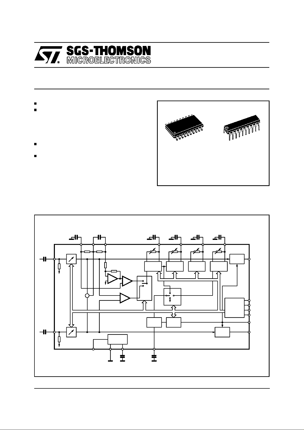
DIGITAL CONTROLLED SURROUNDSOUND MATRIX
1 STEREOINPUT
THREEINDEPENDENT SURROUND MODES
ARE AVAILABLE MOVIE, MUSIC AND SIMULATED
- MUSIC:4 SELECTABLERESPONSES
- MOVIE ANDSIMULATED:
256SELECTABLERESPONSES
TWO INDEPENDENT INPUT ATTENUATORS
IN 0.31dB FORBALANCEFACILITY
ALL FUNCTIONS PROGRAMMABLE VIA SERIAL BUS
SO20
TDA7346
DIP20
DESCRIPTION
The TDA7346 reproduces surround sound by using phase shifters and a signal matrix. Control of
all the functionsis accomplishedby serial bus.
The AC signal setting is obtained by resistor net-
BLOCK DIAGRAM
5.6nF 680nF
LP1
HP1 HP2
100nF
100nF
L
-in
100K
R
-in
100K
RLP1 RHP1
+
R5
-
+
R6
SUPPLY
+
+
L-R
SIM
MOVIE/
MUSIC
ORDERING NUMBER: TDA7346 (DIP20)
TDA7346D (SO20)
works and switches combined with operational
amplifiers.
100nF
PS1
RPS1
PS1
90Hz
LPF
9KHz
4.7nF
PS2
RPS2 RPS3 RPS4
PS2
4KHz
MUSIC
OFF
EFFECT
CONTROL
22nF
PS3
PS3
400Hz
PHASESHIFTER
MOVIE/SIM
22nF
PS4
PS4
400Hz
MIXING
AMP
MIXING
AMP
I2C
BUS
DECODER
LATCHES
L
out
SCL
SDA
DIG GND
ADDR
REAR
R
out
February 1997
VSAGND CREF LP
C5
22µF
1.2nF
D94AU122A
1/14
TDA7346
ABSOLUTE MAXIMUMRATINGS
Symbol Parameter Value Unit
V
T
T
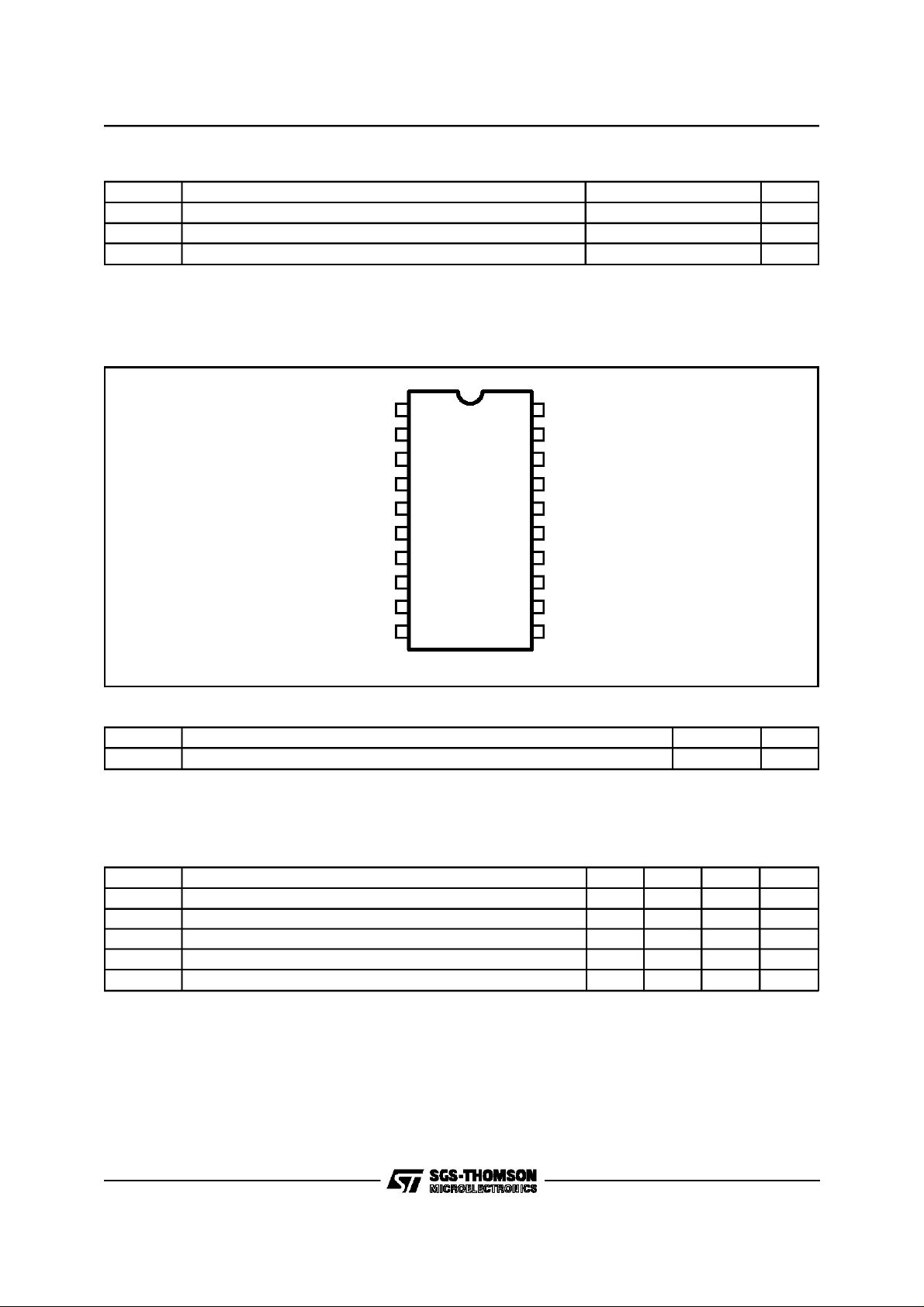
PIN CONNECTION
Operating Supply Voltage 10.5 V
S
Operating Ambient Temperature -40 to 85 °C
amb
Storage Temperature Range -55 to +150 °C
stg
PS1
V
CREF
L
-in
LP
REAR
L
out
SDA
SCL
1
2
S
3
4
5
6
7
8
9 ADDR
19
18
17
16
15
14
13
12
PS220
LP1
HP1
HP2
R
-in
PS3
PS4
R
out
DIG GND 10 AGND11
D94AU128
THERMAL DATA
Symbol Description Value Unit
R
thj-pins
Thermal Resistance Junction-pins Max. 85 °C/W
QUICK REFERENCEDATA
Symbol Parameter Min. Typ. Max. Unit
V
V
CL
THD Total Harmonic Distortion V = 1Vrms f = 1KHz 0.02 0.1 %
S/N Signal to Noise Ratio V
S
2/14
Supply Voltage 7 9 10.2 V
S
Max. input signal handling 2 Vrms
out = 1Vrms (mode = OFF) 106 dB
Channel Separation f= 1KHz 70 dB
C
TEST CIRCUIT
TDA7346
L
out
SCL
SDA
680nF
HP1
18
REAR
6798
C16
17
L
-in
4
0.1µF
C17
V
HP2
S
10µFC1
2
TDA7346
100nF
C2
PS3
22nF
15
C4
PS4
22nF
C5
ELECTRICALCHARACTERISTICS
R
= 600Ω, all controls flat (G = 0),EffectCtrl = -6dB, MODE = OFF; f = 1KHz
G
14
R
out
AGND DIG GND
(refer to the test circuitT
12101113
ADDR
=25°C, VS= 9V, RL= 10KΩ,
amb
unless otherwisespecified)
LP
5
R
16
LP1
19
PS1
1
PS2
20
CREF
3
D93AU040C
1.2nF
C6
0.1µF
-in
C7
5.6nF
C15
100nF
C14
4.7nF
C13
22µF
C3
Symbol Parameter Test Condition Min. Typ. Max. Unit
SUPPLY
V
S
I
S
SVR Ripple Rejection L
Supply Voltage 7 9 10.2 V
Supply Current 10 mA
CH/RCH out
, Mode = OFF 60 80 dB
INPUT STAGE
C
RANGE
A
A
A
V
R
II
V
CL
VMIN
VMAX
STEP
DC
Input Resistance 100 K
Clipping Level THD = 0.3%; Lin orRin 2 2.5 Vrms
THD = 0.3%; Rin + Lin (2) 3.0 Vrms
Control Range 20 dB
Min. Attenuation -1 0 1 dB
Max. Attenuation 20 dB
Step Resolution 0.31 dB
DC Steps adjacent att.step 0 mV
EFFECT CONTROL
C
RANGE
S
STEP
Control Range - 21 - 6 dB
Step Resolution 1 dB
Ω
3/14
TDA7346
ELECTRICAL CHARACTERISTICS
(continued)
SURROUNDSOUND MATRIX
Symbol Parameter Test Condition Min. Typ. Max. Unit
G
D
OFF
GOFF
In-phase Gain (OFF) Mode OFF, Input signal of
LR In-phase Gain Difference
(OFF)
G
MOV1
In-phase Gain (Movie 1)
RPS1, RPS2, RPS3, RPS4 =
POR Preset
G
MOV2
In-phase Gain (Movie 2)
RPS1, RPS2, RPS3, RPS4 =
POR Preset
D
GMOV
LR In-phase Gain Difference
(Movie)
G
MUS1
In-phase Gain (Music 1)
RPS1 = POR PRESET
G
MUS2
In-phase Gain (Music 2)
RPS1 = POR PRESET
D
GMUS
LR In-phase Gain Difference
(Music)
L
MON1
Simulated L Output 1
RPS1, RPS2, RPS3, RPS4 =
POR Preset
L
MON2
Simulated L Output 2
RPS1, RPS2, RPS3, RPS4 =
POR Preset
L
MON3
Simulated L Output 3
RPS1, RPS2, RPS3, RPS4 =
POR Preset
R
MON1
Simulated R Output 1
RPS1, RPS2, RPS3, RPS4 =
POR Preset
R
MON2
Simulated R Output 2
RPS1, RPS2, RPS3, RPS4 =
POR Preset
R
MON3
Simulated R Output 3
RPS1, RPS2, RPS3, RPS4 =
POR Preset
R
LP1
R
PS1
R
PS2
R
PS3
R
PS2
R
HPI
R
LPF
Low Pass Filter Resistance 10 KΩ
Phase Shifter 1 Resistance at POR 17.95 kΩ
Phase Shifter 2 Resistance at POR 8.465 K
Phase Shifter 3 Resistance at POR 18.050 K
Phase Shifter 4 Resistance at POR 18.050 KΩ
High Pass Filter Resistance 60 KΩ
LP Pin Impedance 10 KΩ
1kHz, 1.4 V
L
L
→
in
out
p-p,Rin
→ R
out
Mode OFF, Input signal of
1kHz, 1.4 V
(R
in
→
p-p
R
), (L
out
L
)
→
in
out
Movie mode, Effect Ctrl = -6dB
Input signal of 1kHz, 1.4 V
Rin→ R
out,Lin
→ L
p-p
out
Movie mode, Effect Ctrl = -6dB
Input signal of 1kHz, 1.4 V
Rin→ R
out,Lin
→ L
p-p
out
Movie mode, Effect Ctrl = -6dB
Input signal of 1kHz, 1.4 V
R
(R
in
→
out
)–(L
→
in
p-p
L
)
out
Music mode, Effect Ctrl = -6dB
Input signal of 1kHz, 1.4 V
R
(R
in
→
out
)–(L
→
in
p-p
L
)
out
Music mode, Effect Ctrl = -6dB
Input signal of 1kHz, 1.4 V
Rin→ R
out,Lin
→ L
p-p
out
Music mode, Effect Ctrl = -6dB
Input signal of 1kHz, 1.4 V
(Rin→ R
)–(Lin→ L
out
out
p-p
)
SimulatedMode,EffectCtrl=-6dB
Input signal of 250Hz,
1.4 V
p-p,Rin
and Lin→ L
out
SimulatedMode,EffectCtrl=-6dB
Input signal of 1kHz,
1.4 V
p-p,Rin
and L
L
→
in
out
SimulatedMode, EffectCtrl= 6dB
Input signal of 3.6kHz,
1.4 V
p-p,Rin
and L
L
→
in
out
SimulatedMode,EffectCtrl=-6dB
Input signal of 250Hz,
1.4 V
p-p,Rin
and L
R
→
in
out
SimulatedMode,EffectCtrl=-6dB
Input signal of 1kHz,
1.4 V
p-p,Rin
and Lin→R
out
SimulatedMode,EffectCtrl=-6dB
Input signal of 3.6kHz,
1.4 V
p-p,Rin
and Lin→ R
out
-1.5 0 1.5 dB
-1.5 0 1.5 dB
7dB
8dB
0dB
6dB
7.5 dB
0dB
4.5 dB
– 4.0 dB
7.0 dB
– 4.5 dB
3.8 dB
–20 dB
Ω
Ω
4/14
TDA7346
ELECTRICAL CHARACTERISTICS
(continued)
Symbol Parameter Test Condition Min. Typ. Max. Unit
AUDIO OUTPUTS
V
OCL
R
OUT
V
OUT
Clipping Level d = 0.3% 2 2.5 Vrms
Output resistance 100 200 300 Ω
DC Voltage Level 3.5 3.8 4.1 V
GENERAL
N
O(OFF)
N
O(MOV)
N
O(MUS)
N
O(MON)
d Distorsion Av = 0 ; V
S
C
Output Noise (OFF) BW= 20Hz to 20KHz
R
out
and L
measurement
out
Output Noise (Movie) Mode =Movie ,
B
= 20Hz to 20KHz
W
R
out
andL
measurement
out
Output Noise (Music) Mode = Music ,
B
= 20Hz to 20KHz,
W
R
out
andL
measurement
out
Output Noise (Simulated) Mode = Simulated,
B
= 20Hz to 20KHz
W
R
out
andL
measurement
out
= 1Vrms 0.02 0.1 %
in
8 µVrms
30
30 µVrms
30 µVrms
Channel Separation 70 dB
BUS INPUTS
V
IL
V
IH
I
IN
V
O
Note:
(1) Bassand Treble response: The center frequency and the resonance quality can be choosen by
the external circuitry. A standard first order bass response can be realized by a standard feedback network.
(2) Thepeak voltage of thetwo input signals must be less then
(Lin + Rin)
Input Low Voltage 1V
Input High Voltage 3 V
Input Current -5 +5
Output Voltage SDA
IO= 1.6mA 0.4 0.8 V
Acknowledge
V
S
:
2
peak
• A
V
S
<
Vin
2
Vrms
µ
µ
A
5/14

TDA7346
2
C BUS INTERFACE
I
Data transmission from microprocessor to the
TDA7346 and viceversa takes place through the
2 wires I
2
C BUS interface, consisting of the two
lines SDA and SCL (pull-up resistors to positive
supplyvoltage mustbe connected).
Data Validity
As shown in fig. 3, the data on the SDAline must
be stable during the high period of the clock. The
HIGH and LOW state of the data line can only
change when the clock signal on the SCL line is
LOW.
Start and Stop Conditions
As shown in fig.4 a start condition is a HIGH to
LOW transition of the SDA line while SCL is
HIGH. The stop condition is a LOW to HIGH transition of the SDAline while SCL is HIGH.
Byte Format
Every byte transferred on the SDA line must contain 8 bits. Each byte must be followed by an ac-
Figure 3:
Data Validityon theI
2
CBUS
knowledgebit. The MSBis transferredfirst.
Acknowledge
The master (µP) putsa resistiveHIGH level on the
SDA line during the acknowledge clock pulse (see
fig. 5). The peripheral (audioprocessor) that acknowledges has to pull-down (LOW) the SDA line
during the acknowledge clock pulse, so that the
SDAlineis stableLOWduringthisclockpulse.
The audioprocessor which has been addressed
has to generate an acknowledge after the reception of each byte, otherwisethe SDA line remains
at the HIGH level during the ninth clock pulse
time. In this case the master transmitter can generate the STOP information in order to abort the
transfer.
TransmissionwithoutAcknowledge
Avoiding to detect the acknowledge of the audioprocessor,the µP can usea simplertransmission:
simply it waits one clock without checking the
slave acknowledging,and sends the new data.
This approach of course is less protected from
misworking and decreasesthe noise immunity.
Figure 4:
TimingDiagram of I
2
Figure 5: Acknowledgeon theI
6/14
CBUS
2
CBUS

TDA7346
SOFTWARESPECIFICATION
InterfaceProtocol
The interfaceprotocol comprises:
A startcondition (s)
A chip address byte, containing the TDA7346
TDA7346 ADDRESS
MSB
S110111A0
ACK = Acknowledge
S = Start
P = Stop
MAX CLOCK SPEED 100kbits/s
first byte
LSB MSB LSB MSB LSB
ACK
SOFTWARESPECIFICATION
Chip address
1
MSB
10111A0
address(the 8th bit of the byte must be 0). The
TDA7346must always acknowledgeat the end
of each transmitted byte.
A sequenceof data (N bytes + achnowledge).
A stopcondition (P)
DATA
Data Transferred (N-bytes + Acknowledge)
LSB
ACK
A CHIP ADDRESS
0 DC (HEX)
1 DE (HEX)
DATA
ACK
P
A = Logic level on pin ADDR
A = 1 if ADDR pin = open
A = 0 if ADDR pin = connected to ground
SoftwareSpecification
MSB LSB SUBADDRESS
0 0 A5 A4 A3 A2 A1 A0 INPUT ATTENUATION R
0 1 A5 A4 A3 A2 A1 A0 INPUT ATTENUATION L
1 M1 M0 SURROUND MODES
1 0 0 SIMULATED MODE
1 0 1 MUSIC MODE
1 1 0 MOVIE MODE
11111111OFFMODE
1 M1 M0 1 B3 B2 B1 B0 EFFECT CONTROL
1 M1 M0 0 0 0 C1 C0 PHASE SHIFTER 4 CONTROL
1 M1 M0 0 0 1 C1 C0 PHASE SHIFTER 3 CONTROL
1 M1 M0 0 1 0 D1 D0 PHASE SHIFTER 2 CONTROL
1 M1 M0 0 1 1 E1 E0 PHASE SHIFTER 1 CONTROL
7/14

TDA7346
INPUT ATTENUATION
MSB LSB 0.3125 dB STEPS
I A5A4A3A2A1A0
0 000 0
0 0 0 1 -0.3125
0 0 1 0 -0.625
0 0 1 1 -0.9375
0 1 0 0 -1.25
0 1 0 1 -1.5625
0 1 1 0 -1.875
0 1 1 1 -2.1875
2.5 dB STEPS
0 000 0
0 0 0 1 -2.5
0 010 -5
0 0 1 1 -7.5
0 100 -10
0 1 0 1 -12.5
0 110 -15
0 1 1 1 -17.5
I = 0 AttenuationInput R
I = 1 AttenuationInput L
Example: to program an R input attenuationequal to -11.25 you have to send 00100100
EFFECT CONTROL (-6 / -21dB)
MSB LSB 1dB STEPS
B3 B2 B1 B0
1M1M010000 -6
1M1M010001 -7
1M1M010010 -8
1M1M010011 -9
1M1M010100 -10
1M1M010101 -11
1M1M010110 -12
1M1M010111 -13
1M1M011000 -14
1M1M011001 -15
1M1M011010 -16
1M1M011011 -17
1M1M011100 -18
1M1M011101 -19
1M1M011110 -20
1M1M011111 -21
8/14

TDA7346
PHASE SHIFTER 3, 4
MSB LSB RESISTOR VALUE (KΩ)
C1 C0
1 M1 M0 0 0 F 0 0 12.060
1 M1 M0 0 0 F 0 1 14.450
1 M1 M0 0 0 F 1 0 18.050
1 M1 M0 0 0 F 1 1 39.100
F = 0 Phase Shifter4
F = 1 Phase Shifter3
PHASE SHIFTER 2
MSB LSB RESISTOR VALUE (KΩ)
D1 D0
1M1M001000 5.640
1M1M001001 6.770
1M1M001010 8.465
1M1M001011 18.300
PHASE SHIFTER 1
MSB LSB RESISTOR VALUE (KΩ)
E1 E0
1M1M001100 11.745
1M1M001101 14.150
1M1M001110 17.950
1M1M001111 37.625
Example: to program MOVIE MODE with EFFECT control = -7dB with PHASE SHIFTER resistor =
11.745KΩ, PHASE SHIFTER 2 resistor = 6.77KΩ,
SHIFTER4 resistor= 18.05KΩ,you haveto send in sequence5 bytes:
11010001
11001100
11001001
11000100
11000010
PHASE SHIFTER 3 resistor = 12.06KΩ, PHASE
POWER ON RESET
INPUT ATTENUATION -19.375dB
EFFECT CONTROL -20dB
SURROUND MODE OFF MODE
PHASE SHIFTER 1 RESISTOR VALUE 17.950 K
PHASE SHIFTER 2 RESISTOR VALUE 8.465 K
PHASE SHIFTER 3, 4 RESISTOR VALUE 18.050 K
Ω
Ω
Ω
9/14

TDA7346
PIN:
HP1
LP1
HP2
PIN: Lin,R
PIN:
HP2
V
, R
V
S
20µA
5.5K
60K
D94AU199
, REAR
OUT
S
5.5K
20µA
V
S
10K
60K
GND
D94AU198
in
V
S
HP1
PIN: L
OUT
20µA
PIN:
SCL, SDA
Vref
100K
D94AU123
20µA
D94AU205
PIN:
ADDR
100Ω
V
S
100K
D94AU204
20µA
D94AU212
10/14

TDA7346
PIN:
PIN: C
LP
REF
V
S
D94AU206
V
S
10K
20µA
PIN:
PS3, PS2
PIN: PS2
PS3A
PS4A
V
S
20µA
18.050K
D94AU124
V
S
20µA
PIN:
PS1
PS1A
20K
20K
V
S
20µA
D94AU208
20µA
PIN:
LP1
PS2A
8.465K
D94AU125
V
S
20µA
17.95K
10K
HP1
D94AU126
D94AU211
11/14

TDA7346
SO20 PACKAGEMECHANICAL DATA
DIM.
MIN. TYP. MAX. MIN. TYP. MAX.
A 2.65 0.104
a1 0.1 0.3 0.004 0.012
a2 2.45 0.096
b 0.35 0.49 0.014 0.019
b1 0.23 0.32 0.009 0.013
C 0.5 0.020
c1 45°(typ.)
D 12.6 13.0 0.496 0.512
E 10 10.65 0.394 0.419
e 1.27 0.050
e3 11.43 0.450
F 7.4 7.6 0.291 0.299
L 0.5 1.27 0.020 0.050
M 0.75 0.030
mm inch
S8
(max.)
°
12/14

DIP20 PACKAGE MECHANICAL DATA
TDA7346
DIM.
MIN. TYP. MAX. MIN. TYP. MAX.
a1 0.254 0.010
B 1.39 1.65 0.055 0.065
b 0.45 0.018
b1 0.25 0.010
D 25.4 1.000
E 8.5 0.335
e 2.54 0.100
e3 22.86 0.900
F 7.1 0.280
I 3.93 0.155
L 3.3 0.130
mm inch
Z 1.34 0.053
13/14

TDA7346
Information furnished is believed to be accurate and reliable. However, SGS-THOMSON Microelectronics assumes no responsibility for the
consequences of use of such information nor for any infringement of patents or other rights of third parties which may result from its use. No
license is granted by implication or otherwise under any patent or patentrights of SGS-THOMSON Microelectronics. Specification mentioned
in this publication are subject to change without notice. This publication supersedes and replaces all information previously supplied. SGSTHOMSON Microelectronics products are not authorized for use as critical components in life support devices or systems without express
written approval of SGS-THOMSON Microelectronics.
1997SGS-THOMSON Microelectronics – Printedin Italy– AllRights Reserved
SGS-THOMSON Microelectronics GROUPOF COMPANIES
Australia - Brazil - Canada- China - France -Germany - HongKong - Italy - Japan - Korea - Malaysia- Malta - Morocco - The Netherlands -
Singapore - Spain - Sweden - Switzerland- Taiwan- Thailand - United Kingdom - U.S.A.
14/14
 Loading...