

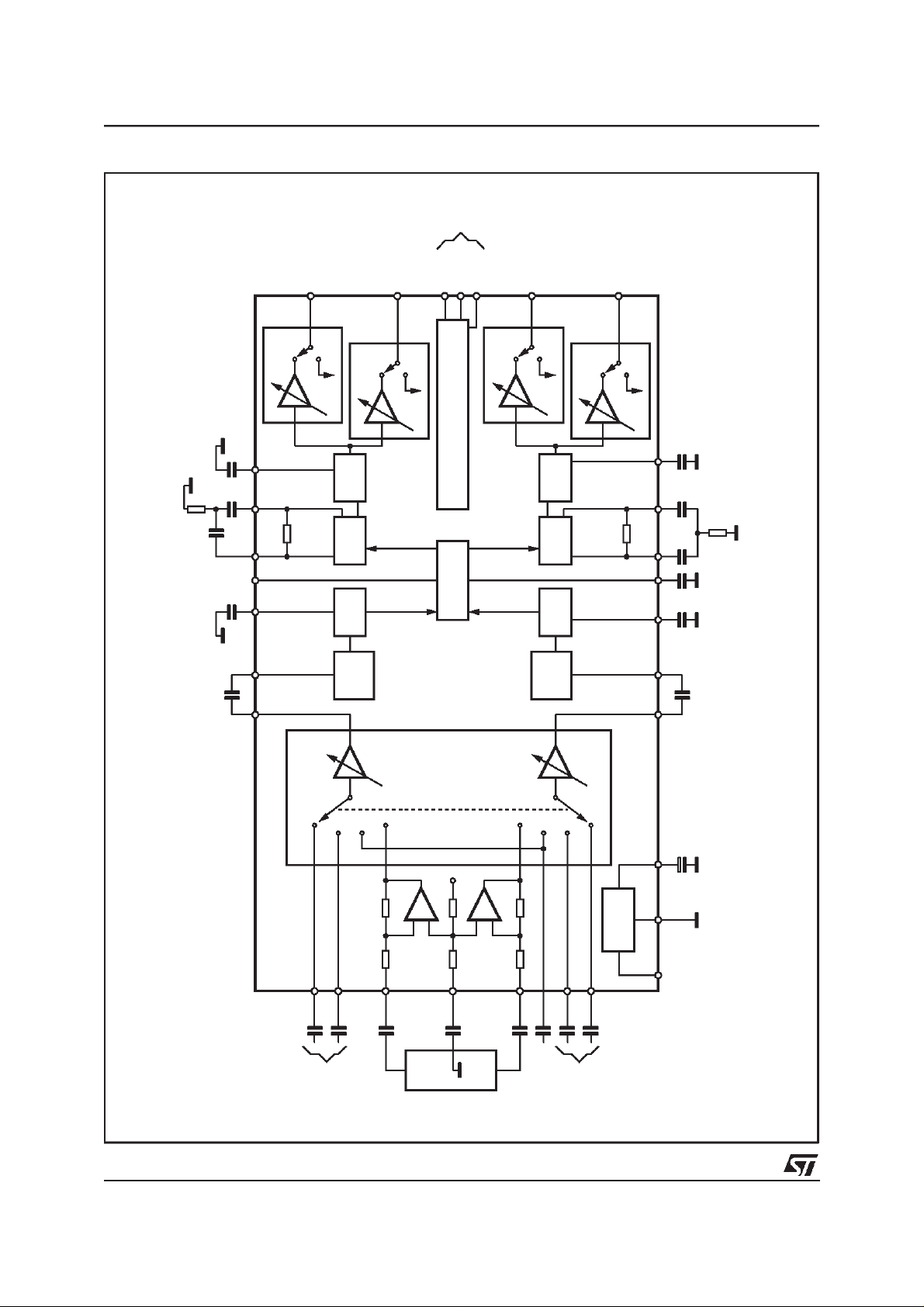
DIGITALLY CONTROLLED AUDIO PROCESSOR
INPUTMULTIPLEXER
- TWOSTEREOANDONEMONO INPUTS
- ONEQUASI DIFFERENTIAL INPUT
- SELECTABLEINPUT GAIN FOR OPTIMAL
ADAPTATIONTO DIFFERENT SOURCES
FULLY PROGRAMMABLE LOUDNESS
FUNCTION
VOLUME CONTROL IN 0.3dB STEPS INCLUDING GAINUP TO20dB
ZERO CROSSINGMUTE, SOFT MUTE AND
DIRECT MUTE
BASS AND TREBLE CONTROL
FOURSPEAKERATTENUATORS
- FOURINDEPENDENT SPEAKERS
CONTROLIN 1.25dBSTEPSFOR
BALANCEAND FADER FACILITIES
- INDEPENDENTMUTE FUNCTION
ALL FUNCTIONS PROGRAMMABLE VIA SE-
2
RIAL I
DESCRIPTION
The audioprocessor TDA7342 is an upgrade of
the TDA731X audioprocessorfamily.
Due to a highly linear signal processing, using
CMOS-switching techniques instead of standard
CBUS
TDA7342
TQFP 32
ORDERING NUMBER: TDA7342
bipolar multipliers, very low distortion and very
low noise are obtained.Several new features like
softmute, and zero-crossing mute are implemented.
The soft Mute function can be activated in two
ways:
1 Via serial bus(Mute byte, bit D0)
2 Directly on pin 21 through an I/O line of the
microcontroller
Very low DC stepping is obtained by use of a
BICMOStechnology.
November 1999
1/14
TDA7342
BLOCK DIAGRAM
BUS
R2
4.7K
C17 100nF
C11
C19 2.7nF
TREBLE(L)
C18
100nF
BIN(L)
BOUT(L)
SM
LOUD(L)
C13 47nF
OUT(L) IN(L)
32
18 17
21
9
16 15
ATT
SPKR
25
OUT
LEFT FRONT
MUTE
SPKR
TREBLE
BASS
VOL
LOUD+
+
ZERO
CROSS
ATT
MUTE
23
OUT
LEFT REAR
MUTE
SCL
SDA
282726
SERIAL BUS DECODER + LATCHES
SOFT
MUTE
DIGGND
SPKR
ATT
24
OUT
RIGHT FRONT
MUTE
TREBLE
BASS
LOUD+
+
ZERO
CROSS
VOL
MUTE
ATT
SPKR
OUT
RIGHT REAR
22
D94AU104B
MUTE
C16
TREBLE(R)
C15
C14
BOUT(R) BIN(R)
20 19 1
CSMOUT(R)CREF IN(R)
CSM
C12
LOUD(R)
24
314
2.7nF
100nF
100nF
47nF
47nF
C10
4.7K
R1
2/14
INPUT
+ GAIN
SELECTOR
L1
L2
13
12
L1
L2
C1
LEFT
M
INPUTS
L3
11
L3
C2
C6
10
CD GND
CD
R3
M
8
5
M
R3
C3
C7
C8
MONO INPUT
R1
R2
SUPPLY
7
6
R1
R2
C5
C4
RIGHT
INPUTS
10µFC9
30 31 29
S
V
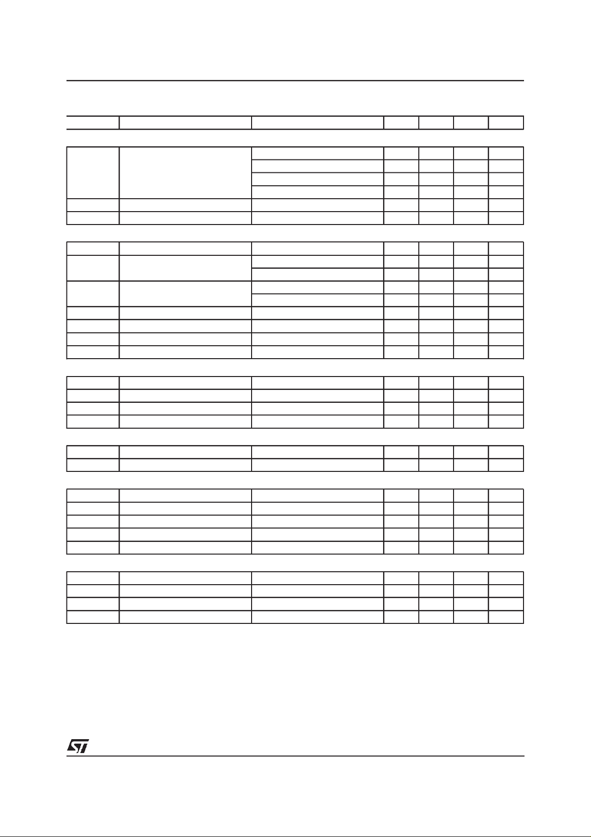
ABSOLUTE MAXIMUM RATINGS
Symbol Parameter Value Unit
V
S
T
amb
T
stg
Operating Supply Voltage 10.5 V
Operating Ambient Temperature -40 to 85 °C
Storage Temperature Range -55 to 150 °C
PIN CONNECTION
S
TR L
V
TR R
IN R
OUT R
LOUD R
IN R3
IN R2
IN R1
MONO
GNDSMCREF
32 3031 29 28 27 26 25
1
2
3
4
5
6
7
8
910
11 12 13 14 15 16
SCL
SDA
DIG GND
OUT LF
24
OUT RF
23
OUT LR
22
OUT RR
21
BOUT R
20
BIN R
19
BOUT L
18
BIN L
17
TDA7342
IN L
IN L3
LOUD L
CD GND
CSM
IN L2
IN L1
D94AU105A
OUT L
THERMAL DATA
Symbol Parameter Value Unit
R
th j-amb
Thermal ResistanceJunction-pins 150 °C/W
QUICK REFERENCE DATA
Symbol Parameter Min. Typ. Max. Unit
V
S
V
CL
THD Total Harmonic DistortionV = 1Vrms f = 1KHz 0.01 0.08 %
S/N Signalto Noise Ratio 106 dB
S
C
Supply Voltage 6 9 10.2 V
Max. input signal handling 2.1 2.6 Vrms
Channel Separation f = 1KHz 100 dB
Volume Control 0.3dB step -59.7 20 dB
Treble Control 2dB step -14 +14 dB
Bass Control 2dB step -10 +18 dB
Fader and Balance Control 1.25dBstep -38.75 0 dB
Input Gain 3.75dB step 0 11.25 dB
Mute Attenuation 100 dB
3/14
TDA7342
ELECTRICALCHARACTERISTICS (VS= 9V; RL= 10KΩ;Rg=50Ω;T
=25°C; all gains= 0dB;
amb
f = 1KHz. Refer to the test circuit, unless otherwisespecified.)
Symbol Parameter Test Condition Min. Typ. Max. Unit
INPUTSELECTOR
G
G
G
R
V
S
R
I MIN
I MAX
step
e
V
CL
L
N
DC
Input Resistance 70 100 130 KΩ
I
Clipping Level d ≤ 0.3% 2.1 2.6 V
Input Separation 80 100 dB
I
Output Load Resistance 2 KΩ
Minimum InputGain -0.75 0 0.75 dB
Maximum Input Gain 10.25 11.25 12.25 dB
Step Resolution 2.75 3.75 4.75 dB
Input Noise 20Hz to 20 KHz unweighted 2.3
DC Steps Adiacent Gain Steps 1.5 10 mV
to G
G
IIN
IMAX
3mV
DIFFERENTIAL INPUT ( IN 3)
R
CMRR Common Mode Rejection Ratio V
d Distortion V
e
IN
DIFF Differential Gain D6 = 0 -1 0 1 dB
G
Input Resistance Input selector BIT D6 = 0 (0dB) 10 15 20 K
I
Input selector BIT D6 = 1(-6dB) 14 20 30 K
CM
=1V
; f =1KHz 48 75 dB
RMS
f = 10KHz 45 70 dB
=1V
I
RMS
0.01 0.08 %
Input Noise 20Hz to 20KHz; Flat; D6 = 0 5 µV
D6 = 1 -7 -6 -5 dB
RMS
V
µ
Ω
Ω
VOLUMECONTROL
R
G
MAX
A
MAX
A
STEPC
A
STEPF
E
A
E
V
DC
Input Resistance 35 50 KΩ
I
Maximum Gain 18.75 20 21.25 dB
Maximum Attenuation 57.7 59.7 62.7 dB
Step Resolution Coarse Atten. 0.5 1.25 2.0 dB
StepResolution FineAttenuation 0.11 0.31 0.51 dB
Attenuation Set Error G = 20 to -20dB -1.25 0 1.25 dB
Tracking Error 2dB
t
DC Steps Adiacent Attenuation Steps -3 0 3 mV
LOUDNESS CONTROL
R
A
MAX
A
step
Internal Resistor Loud = On 35 50 65 K
I
Maximum Attenuation 17.5 18.75 20.0 dB
Step Resolution 0.5 1.25 2.0 dB
G = -20 to -58dB -3 2 dB
From 0dB to A
MAX
0.5 5 mV
Ω
4/14
TDA7342
ELECTRICALCHARACTERISTICS (continued.)
Symbol Parameter Test Condition Min. Typ. Max. Unit
ZEROCROSSINGMUTE
V
TH
A
MUTE
V
DC
SOFTMUTE
A
MUTE
T
DON
T
DOFF
V
THSM
R
INT
V
SMH
V
SML
BASS CONTROL
B
BOOST
B
CUT
A
step
R
g
TREBLECONTROL
C
RANGE
A
step
SPEAKERATTENUATORS
C
RANGE
A
step
A
MUTE
E
A
V
DC
AUDIO OUTPUT
V
clip
R
L
R
O
V
DC
Zero Crossing Threshold
(note 1)
WIN = 11 20 mV
WIN = 10 40 mV
WIN = 01 80 mV
WIN = 00 160 mV
Mute Attenuation 80 100 dB
DC Step 0dBto Mute 0 3 mV
Mute Attenuation 45 60 dB
ON Delay Time C
=22nF;0 to-20dB; I =I
CSM
CSM =22nF; 0 to -20dB; I = IMIN 20 35 55 ms
C
0.7 1 1.7 ms
MAX
OFF Current VCSM = 0V;I = IMAX 25 50 75 µA
CSM =0V; I = IMIN 1 µA
V
Soft MuteThreshold 1.5 2.5 3.5 V
Pullup Resistor (pin 21) (note 2) 35 50 65 K
(pin 21) Level High 3.5 V
(pin 21) Level Low Soft Mute Active 1 V
Max Bass Boost 15 18 20 dB
Max Bass Cut -8.5 -10 -11.5 dB
Step Resolution 1 2 3 dB
Internal Feedback Resistance 45 65 85 KΩ
Control Range
13
±
14
±
15 dB
±
Step Resolution 1 2 3 dB
Control Range 35 37.5 40 dB
Step Resolution 0.5 1.25 2.00 dB
Output Mute Attenuation Data Word = XXX11111 80 100 dB
Attenuation Set Error 1.25 dB
DC Steps Adjacent Attenuation Steps 0 3 mV
Clipping Level d = 0.3% 2.1 2.6 Vrms
Output Load Resistance 2 K
Output Impedance 30 100 Ω
DC Voltage Level 3.5 3.8 4.1 V
Ω
Ω
5/14

TDA7342
ELECTRICALCHARACTERISTICS (continued)
Symbol Parameter Test Condition Min. Typ. Max. Unit
GENERAL
V
CC
I
CC
PSRR Power Supply Rejection Ratio f = 1KHz 60 80 dB
e
NO
E
S/N Signal to Noise Ratio All Gains = 0dB; V
S
C
d Distortion V
BUS INPUTS
V
IL
V
lN
I
lN
V
O
Supply Voltage 6 9 10.2 V
Supply Current 5 10 15 mA
B = 20 to 20kHz ”A” weighted 65 dB
Output Noise OutputMuted(B= 20to20kHzflat) 2.5 µV
All Gains0dB(B= 20to20kHzflat) 5 15 µV
Total Tracking Error AV = 0 to -20dB 0 1 dB
t
= -20to -60dB 0 2 dB
A
V
O
=1V
rms
106 dB
Channel Separation 80 100 dB
=1V 0.01 0.08 %
IN
Input Low Voltage 1V
Input High Voltage 3 V
Input Current VIN = 0.4V -5 5
Output Voltage SDA
IO= 1.6mA 0.4 0.8 V
Acknowledge
A
µ
Note 1: WIN represents the MUTE programming bit pair D6,D5for the zero crossing window threshold
Note 2: Internallpullup resistor toVs/2; ”LOW” = softmuteactive
6/14

TDA7342
2
C BUS INTERFACE
I
Data transmission from microprocessor to the
TDA7342 and viceversa takes place thru the 2
wires I
2
C BUS interface, consisting of the two
lines SDA and SCL (pull-up resistors to positive
supply voltage must be externallyconnected).
Data Validity
As shown in fig. 3, thedata on the SDA line must
be stable during the high period of the clock. The
HIGH and LOW state of the data line can only
change when the clock signal on the SCL line is
LOW.
Start and Stop Conditions
As shown in fig.4 a start condition is a HIGH to
LOW transition of the SDA line while SCL is
HIGH. The stop condition is a LOW to HIGH transition of the SDA line while SCL is HIGH.
A STOP conditions must be sent before each
START condition.
Byte Format
Every byte transferred to the SDA line must conFigure 3: Data Validity on the I
2
CBUS
tain 8 bits. Each byte must be followed by an acknowledgebit. The MSB is transferredfirst.
Acknowledge
The master(µP)putsa resistiveHIGHlevelon the
SDA line during the acknowledgeclock pulse (see
fig. 5). The peripheral (audioprocessor) that acknowledges has to pull-down (LOW) the SDA line
during the acknowledge clock pulse, so that the
SDAlineisstableLOWduringthis clockpulse.
The audioprocessor which has been addressed
hasto generateanacknowledgeafterthereception
ofeachbyte, otherwisethe SDAlineremainsatthe
HIGHlevelduringthe ninthclock pulsetime.In this
case the master transmitter can generate the
STOPinformation in orderto abortthetransfer.
Transmissionwithout Acknowledge
Avoiding to detect the acknowledge of the audioprocessor, the µP can use a simplier transmission: simply it waits one clock without checking
the slave acknowledging, and sends the new
data.
This approach of course is less protected from
misworkingand decreasesthe noise immunity.
Figure 4: Timing Diagram of I2CBUS
2
Figure 5: Acknowledge on the I
CBUS
7/14

TDA7342
SOFTWARESPECIFICATION
Interface Protocol
The interface protocol comprises:
A start condition (s)
read/writetransmission)
A subaddressbyte.
A sequenceof data (N-bytes+ acknowledge)
A stopcondition (P)
A chip address byte,(the LSB bit determines
CHIP ADDRESS SUBADDRESS DATA 1 to DATA n
MSB LSB MSB LSB MSB LSB
S1000100R/W
ACK X X X I A3 A2 A1 A0 ACK DATA ACK P
ACK = Acknowledge
S = Start
P = Stop
I = Auto Increment
X = Not used
MAX CLOCK SPEED500kbits/s
AUTO INCREMENT
If bit I in the subaddressbyte is set to ”1”,the autoincrementof the subaddressis enabled
SUBADDRESS (receivemode)
MSB LSB FUNCTION
X X X I A3A2A1A0
0 0 0 0 Input Selector
0 0 0 1 Loudness
0 0 1 0 Volume
0 0 1 1 Bass, Treble
0 1 0 0 Speaker Attenuator LF
0 1 0 1 Speaker Attenuator LR
0 1 1 0 Speaker Attenuator RF
0 1 1 1 Speaker Attenuator RR
1 0 0 0 Mute
TRANSMITTED DATA
Send Mode
MSB LSB
X X X X X SM ZM X
ZM = Zero crossingmuted (HIGH active)
SM =Soft mute activated(HIGH active)
X = Not used
The transmitted data is automaticallyupdated aftereach ACK.
Transmissioncan be repeated without newchipaddress.
8/14

DATA BYTE SPECIFICATION
X = not relevant; set to ”1” during testing
Input Selector
TDA7342
MSB LSB
D7 D6 D5 D4 D3 D2 D1 D0
0 1 0 0 0 IN 3 (differential input)
0 1 001IN2
0 1 010IN1
0 1 0 1 1 AM mono
0 1 1 0 0 not used
0 1 1 0 1 not used
0 1 1 1 0 not allowed
0 1 1 1 1 not allowed
0 1 0 0 11.25dB gain
0 1 0 1 7.5dB gain
0 1 1 0 3.75dB gain
0 1 1 1 0dB gain
0 0dB differential input gain ( IN3 )
1 -6dB differential input gain ( IN3 )
FUNCTION
For example to select the IN 2 inputwith a gainof 7.5dB the Data Byte is: X X 101001
Loudness
MSB LSB
D7 D6 D5 D4 D3 D2 D1 D0
XXX00000 0dB
X X X 0 0 0 0 1 -1.25dB
X X X 0 0 0 1 0 -2.5dB
X X X 0 0 0 1 1 -3.75dB
X X X 0 0 1 0 0 -5dB
X X X 0 0 1 0 1 -6.25dB
X X X 0 0 1 1 0 -7.5dB
X X X 0 0 1 1 1 -8.75dB
X X X 0 1 0 0 0 -10dB
X X X 0 1 0 0 1 -11.25dB
X X X 0 1 0 1 0 -12.5dB
X X X 0 1 0 1 1 -13.75dB
X X X 0 1 1 0 0 -15dB
X X X 0 1 1 0 1 -16.25dB
X X X 0 1 1 1 0 -17.5dB
X X X 0 1 1 1 1 -18.75dB
X X X 1 D3 D2 D1 D0 Loudness OFF (1)
FUNCTION
For example to select -17.5dBattenuation,loudnessOFF, the Data Byte is: X X X1 1 1 1 0
NOTE 1:
If the loudness is switched OFF, the loudness stage is actinglike a volume attenuator with flat frequency response. D0 to D3 determine the
attenuation level.
9/14

TDA7342
Mute
MSB LSB
D7 D6 D5 D4 D3 D2 D1 D0
1 Soft Mute On
0 1 Soft Mute withfast slope (I = I
1 1 Soft Mute withslow slope (I= I
1 Direct Mute
0 1 Zero Crossing Mute On
00
1 Zero Crossing Mute and Pause Detector Reset
0 0 0 160mV ZC Window Threshold (WIN = 00)
0 1 0 80mV ZC Window Threshold (WIN = 01)
1 0 0 40mV ZC Window Threshold (WIN = 10)
1 1 0 20mV ZC Window Threshold (WIN = 11)
0 Nonsymmetrical BassCut (note 4)
1 Symmetrical Bass Cut
Zero Crossing Mute Off (delayed until next zero
crossing)
An additionaldirect mute functionis included in the SpeakerAttenuators.
Note 4: Bass cut forvery low frequencies;should not be usedat +16 and +18dB bass boost (DC gain)
FUNCTION
MAX
MIN
)
)
Speaker Attenuators
MSB LSB
D7 D6 D5 D4 D3 D2 D1 D0
XXX 000 0dB
X X X 0 0 1 -1.25dB
X X X 0 1 0 -2.5dB
X X X 0 1 1 -3.75dB
XXX 100 -5dB
X X X 1 0 1 -6.25dB
X X X 1 1 0 -7.5dB
X X X 1 1 1 -8.75dB
XXX00 0dB
X X X 0 1 -10dB
X X X 1 0 -20dB
X X X 1 1 -30dB
X X X 1 1 1 1 Speaker Mute
SPEAKER ATTENUATOR LF, LR, RF, RR
1.25dB step
10dB step
For example an attenuationof 25dB on a selected output is given by: X X X1 0 1 0 0
10/14

Bass Treble
MSB LSB
D7 D6 D5 D4 D3 D2 D1 D0
0 0 0 0 -14dB
0 0 0 1 -12dB
0 0 1 0 -10dB
0 0 1 1 -8dB
0 1 0 0 -6dB
0 1 0 1 -4dB
0 1 1 0 -2dB
0111 0dB
1111 0dB
1110 2dB
1101 4dB
1100 6dB
1011 8dB
1 0 1 0 10dB
1 0 0 1 12dB
1 0 0 0 14dB
0 0 1 0 -10dB
0 0 1 1 -8dB
0 1 0 0 -6dB
0 1 0 1 -4dB
0 1 1 0 -2dB
0111 0dB
1111 0dB
1110 2dB
1101 4dB
1100 6dB
1011 8dB
1 0 1 0 10dB
1 0 0 1 12dB
1 0 0 0 14dB
0 0 0 1 146B
0 0 0 0 18dB
FUNCTION
TREBLE STEP
BASS STEPS
TDA7342
For example 12dB Trebleand-8dB Bassgive the following DATABYTE: 0 0 1 1 1 0 0 1
11/14

TDA7342
Volume
MSB LSB
D7 D6 D5 D4 D3 D2 D1 D0
0.31dB Fine AttenuationSteps
0 0 0dB
0 1 -0.31dB
1 0 -0.62dB
1 1 -0.94dB
1.25dB Coarse Attenuation Steps
000 0dB
0 0 1 -1.25dB
0 1 0 -2.5dB
0 1 1 -3.75dB
1 0 0 -5dB
1 0 1 -6.25dB
1 1 0 -7.5dB
1 1 1 -8.75dB
10dB Gain / Attenuation Steps
000 20dB
001 10dB
010 0dB
0 1 1 -10dB
1 0 0 -20dB
1 0 1 -30dB
1 1 0 -40dB
1 1 1 -50dB
FUNCTION
For example to select -47.81dB Volume the Data Byteis: 1 1 01 1 0 0 1
Power on RESET:AllBytes Set to 1 11 1 11 1 0
12/14

TDA7342
DIM.
MIN. TYP. MAX. MIN. TYP. MAX.
A 1.60 0.063
A1 0.05 0.15 0.002 0.006
A2 1.35 1.40 1.45 0.053 0.055 0.057
B 0.30 0.37 0.45 0.012 0.015 0.018
C 0.09 0.20 0.004 0.008
D 9.00 0.354
D1 7.00
D3 5.60 0.220
e 0.80 0.031
E 9.00 0.354
E1 7.00
E3 5.60 0.220
L 0.45 0.60 0.75 0.018 0.024 0.030
L1 1.00 0.039
K 0°(min.), 7°(max.)
mm inch
0.276
0.276
OUTLINE AND
MECHANICAL DATA
TQFP32
D
D1
D3
1724
25
B
32
1
16
E3
9
8
E1
E
0.10mm
.004
SeatingPlane
e
L1
L
A1
B
C
A
A2
K
TQFP32
13/14

TDA7342
Purchase of I2C Componentsof STMicrolectronics, conveys a license under the Philips I2C Patent
Rights to use these components in an I
2
C system, provided that the system conforms to the I2C
Standard Specificationsas definedby Philips.
Information furnished is believed to be accurate and reliable. However, STMicroelectronics assumes no responsibility for the consequences
of use of such information nor for any infringement of patents or other rights of third parties which may result from its use. No license is
granted by implication or otherwise under any patent or patent rights of STMicroelectronics. Specification mentioned in this publication are
subject to change without notice. This publicationsupersedes and replaces all informationpreviously supplied. STMicroelectronics products
are not authorized for use as critical components in life support devices or systems without express written approval of STMicroelectronics.
The ST logo is a registered trademark of STMicroelectronics
1999 STMicroelectronics – Printed in Italy – AllRights Reserved
STMicroelectronics GROUP OF COMPANIES
Australia - Brazil - China- Finland - France - Germany - HongKong - India - Italy - Japan - Malaysia - Malta- Morocco -
Singapore - Spain - Sweden - Switzerland - UnitedKingdom - U.S.A.
14/14
 Loading...