

AUDIOPROCESSOR:
MUTE, SOFT MUTE AND ZERO CROSSING
MUTE
ONE DIFFERENTIAL, TWO STEREO AND
TWO MONO INPUTS
DIFFERENTIAL PHONEINPUT
VOLUME, BASS, TREBLE AND LOUDNESS
CONTROL
FOUR SPEAKER ATTENUATORS WITH IN-
DEPENDENTATTENUATION CONTROL
STEREODECODER:
ROLL-OFFADJUSTMENT
ADJUSTMENT FREE INTEGRATED 456KHz
VCO
HIGHCUT CONTROL
STEREOBLEND
NOISE BLANKER:
INTEGRATEDHIGH-PASSFILTER
NOISE RECTIFIER OUTPUT FOR QUALITY
DETECTION
PROGRAMMABLETRIGGERTHRESHOLD
DEVIATION AND FIELD STRENGTH DE-
PENDENT TRIGGERADJUSTMENT
PAUSE DETECTOR:
PROGRAMMABLETHRESHOLD
ALLFUNCTIONS PROGRAMMABLEVIA I
DESCRIPTION
The TDA7340G I
processor contains all signal processing blocks of
2
C bus controlled audio signal
2
CBUS
TDA7340G
AUDIO SIGNAL PROCESSOR
PQFP44
ORDERING NUMBER: TDA7340G
a high performance car radio, including audioprocessor, stereodecoder, noise blanker, pause
detectorand differentmute functions.
The use of BICMOS technology allows the implementation of several filter functions with switched
capacitor techniques like fully integrated, adjustment free PLL Loop filter, pilot detector with integratorand pilotcancellation.
This minimizes the number of external components.
Due to a highly linear signal processing, using
CMOS-switching techniques instead of standard
bipolar multipliers, very low distortion and very
low noise are obtained also in the stereodecoder
part. The audioprocessor contains several new
features like softmute, zero-crossing mute and
pausedetector.
Very low DC stepping is obtained by use of a
BICMOStechnology.
September 1999
1/27
TDA7340G
AUDIO PROCESSORPART
FEATURES:
Input Multiplexer:
DIFFERENTIAL CD STEREOINPUT
CASSETTESTEREOINPUT
FM STEREO INPUT FROM STEREODE-
CODER
AM INPUT:
MONO OR STEREO MODE (PROGRAMMABLE)
BEEP INPUT(ONLY IN AM MONO MODE)
TELEPHONEDIFFERENTIAL MONOINPUT
GAIN PROGRAMMABLE IN 3 x 3.75dB
STEPS
Loudness:
FULLY PROGRAMMABLE
15 x 1.25dB STEPS
Volume Control:
1.25dBCOARSE ATTENUATOR
0.31dBFINE ATTENUATORS
MAX GAIN 20dB
MAX ATTENUATION 59.7dB (PLUS LOUD-
NESS)
Bass Control
±7 x 2dB STEPS
2nd ORDER SYMMETRICAL OR NON SYM-
METRICAL CUTFREQUENCYRESPONSE
Treble Control
±7 x 2dB STEPS
Speaker Control
4 INDEPENDENT SPEAKER CONTROL IN
1.25dB STEPS
CONTROLRANGE 37.5dB
INDEPENDENT SPEAKER MUTE
Mute Functions
DIRECTMUTE
ZERO CROSSING MUTE WITH PROGRAM-
MABLETHRESHOLD
SOFT MUTE WITH EXTERNAL DEFINED
SLOPE
SOFT MUTE VIA I
2
C BUS OR EXTERNALLY
CONTROLLED
Pause Detector
PROGRAMMABLETHRESHOLD
DELAY TIME DEFINED BY AN EXTERNAL
CAPACITOR
STEREODECODERPART
FEATURES:
INTERNALLY ADJUSTABLE ROLL-OFF
COMPENSATION(I
2
C BUS CONTROLLED)
INTEGRATEDPILOTCANCELLATION
ON CHIP FILTER FOR PILOT DETECTOR
ANDPLL
ADJUSTMENT FREE VOLTAGE CONTROL-
LED OSCILLATOR
AUTOMATIC PILOT DEPENDENT
MONO/STEREOSWITCHING
VERY HIGH INTERMODULATION AND IN-
TERFERENCE SUPPRESSION
2
C BUS CONTROLLED (STD OFF, FORCED
I
MONO,STEREO)
HIGHCUT CONTROL
STEREOBLEND
NOISE BLANKER PART
FEATURES:
INTERNAL2nd ORDER HIGH-PASSFILTER
NOISE RECTIFIER OUTPUT FOR SIGNAL
QUALITYDETECTION
PROGRAMMABLETRIGGER THRESHOLD
TRIGGER THRESHOLD DEPENDENT ON
HIGHFREQUENCY NOISE
BLANKING TIME PROGRAMMABLE BY EX-
TERNALCAPACITOR
VERY LOW OFFSET CURRENT DURING
HOLD TIME DUE TO OPAMPS WITH MOS
INPUTS
LEVEL INPUT FOR ADDITIONAL SPIKE DETECTION ON FIELD STRENGTH WITH INTERNAL 1st ORDER + 20KHz HIGH PASS
FILTER
NOISE RECTIFIER OUTPUT FOR QUALITY
DETECTION
CIRCUITS FOR DEVIATION AND FIELD
STRENGTH DEPENDENT TRIGGER ADJUSTMENT
2/27
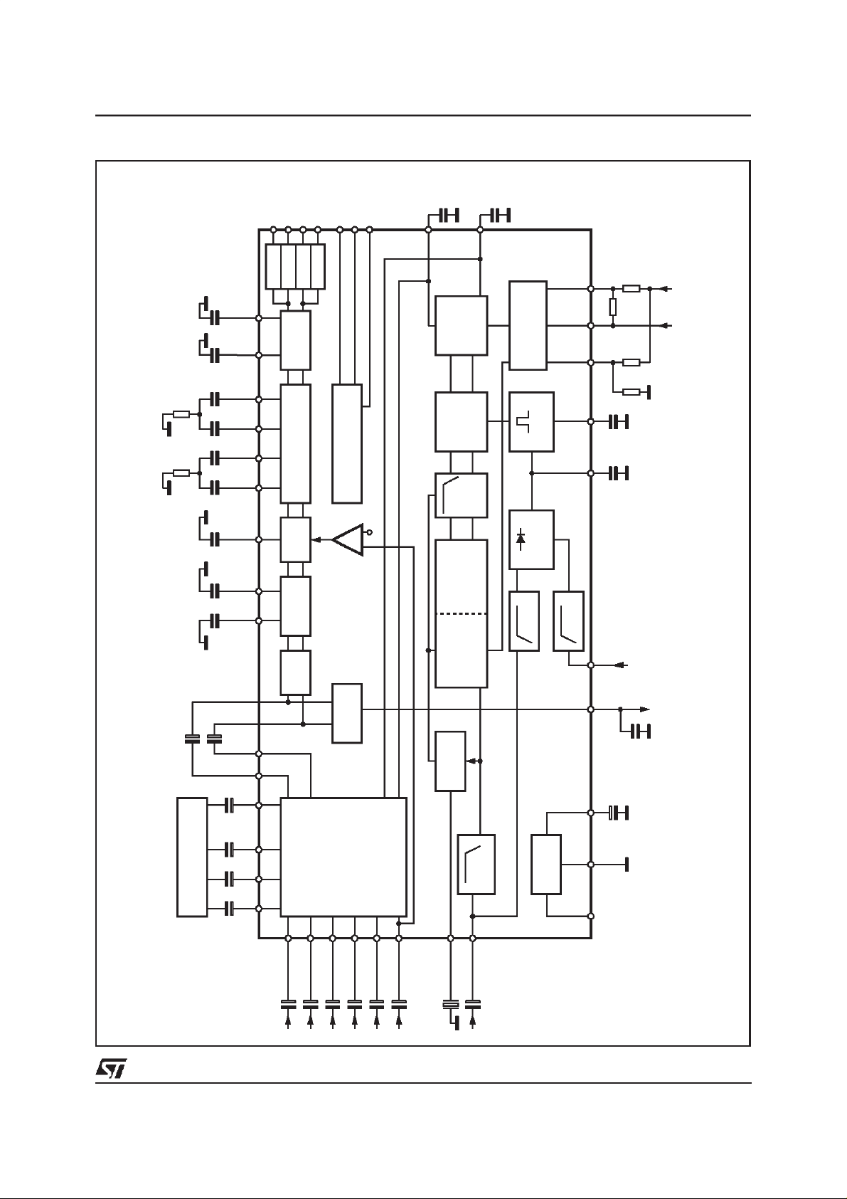
BLOCK DIAGRAM
TDA7340G
6.2K
6.2K
1µFC2
1nF
OUT LR
OUT LF
OUT RR
OUT RF
SCL
SDA
DIGGND
OUT LF
OUT LR
C12
2.7nF
C11
2.7nF
C7 C8 C9 C10
C6
47nF
C5
47nF
C4
47nF
BOUT R TR L TR R
BIN R
BOUT L
BIN L
LOUD L LOUD R CSM
IN L
IN R
C3
1µF
OUT L
OUT R
R2
4x
100nF
R1
OUT RF
OUT RR
TREBLE
BASS
SOFT
MUTE
VOLUME +
LOUDNESS
MUTE
C BUS
2
I
+-
PAUSE
1.4V
FM R
HC L
DEMODULATOR
PLL
FM L
C13
HC R
CUT
HIGH
CONTROL
NOISE
BLANKER
LP
25KHz
19KHz
CANCELLATION
AND
AMPLITUDE ADJ
456KHz
1nF
C14
LEVEL
CONTROL
PULSE
FORMER
PEAK
DETECTOR
HP
D95AU329A
47K
R5
68K
47K
VSB VR VHCC
C17
470pF
C16
47nF
HP
LEVEL PEAK TBLANK
TDA7340G
C1
R6
R4
R3
100K
field strength
C15
47nF
reflevel level
(*)
CD
CREF PAUSE
MUX
4x
CD L+ CD R+
4.7µF
AM_L
AM_R
(BEEP)
CASS L
CASS R
(AM MONO)
6x
1µF
PHONE IN
PHONE GND
VCO
MPX
LP
80KHz
1µF
SUPPLY
GND
S
V
(*) NETWORK TO BE ADAPTED TO THE SPECIFIC REQUESTS FOR STEREO BLEND AND HIGH CUT CONTROL
3/27

TDA7340G
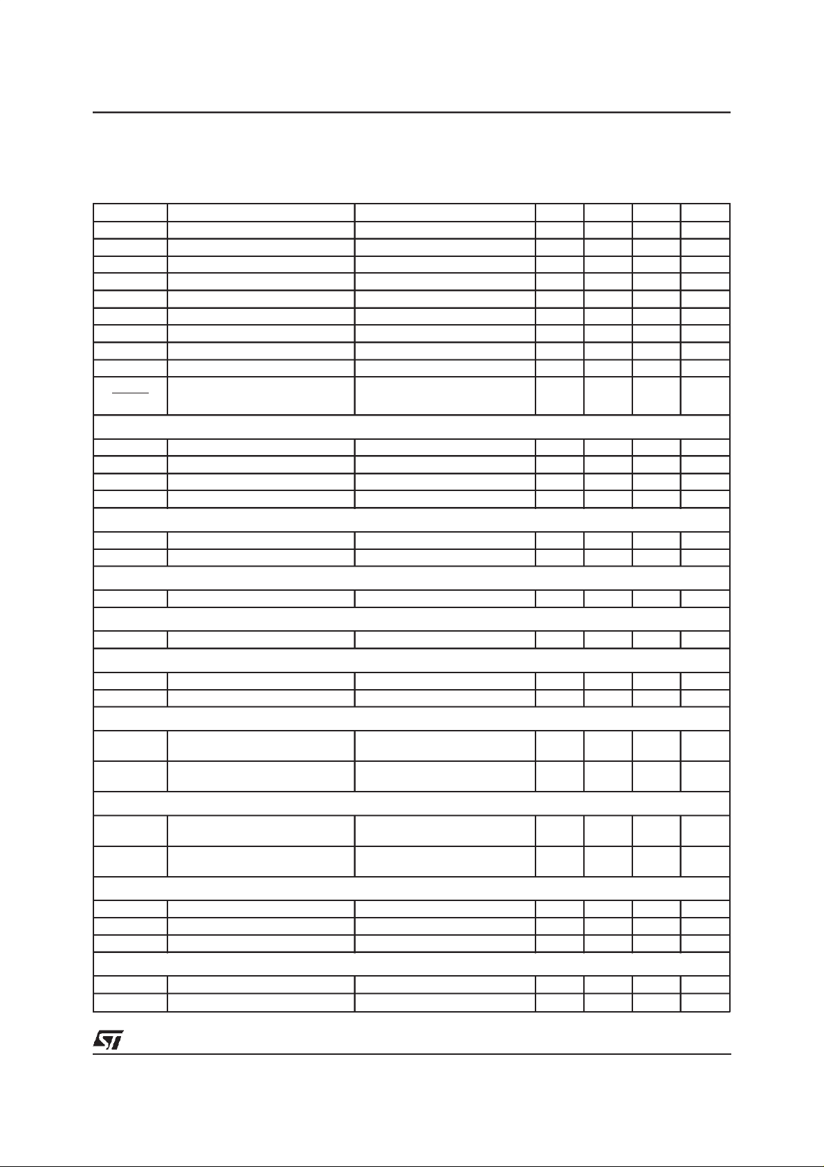
ABSOLUTE MAXIMUM RATINGS
Symbol Parameter Value Unit
V
S
T
amb
T
stg
PIN CONNECTION
Operating Supply Voltage 10.5 V
Operating Temperature Range -40 to 85 °C
Storage Temperature Range -55 to 150 °C
IN R
OUT R
BIN R
BOUT R
BOUT L
BIN L
AM_L (BEEP)
AM_R (AM MONO)
CASS L
CASS R
TR R
44 43 42 41 3940 38 37 36 35 34
OUT L
IN L
CREF
LOUD L
LOUD R
GND
DIGGND
VDD
CSM
SCL
SDA
1
2
3
4
5
6
7
8
9
10
12 13 14 15 16
VCO
PAUSE
PEAK
TBLANK
TDA7340P
(PQFP44)
LEVEL
171118 19 20 21 22
HCL
VSB
HCR
33
TR L
32
CD L+
31
CD L-
30
CD R-
29
CD R+
28
PHON IN
27
PHON GND
26
OUT LF
25
OUT RF
24
OUT LR
23
OUT RR
VR
D94AU055A
MPX
VHCC
THERMAL DATA
Symbol Parameter Value Unit
R
th j-pins
Thermal Resistance Junction-pins max 85 °C/W
ELECTRICALCHARACTERISTICS(VS = 9V; Tamb =25°C; RL = 10KΩ; all gains= 0dB;f = 1KHz;
REF =22µF; unless otherwisespecified, referto the Test Circuit.)
C
Symbol Parameter Test Condition Min. Typ. Max. Unit
SUPPLY
V
S
I
S
SVR Ripple Rejection Audioprocessor 70 90 dB
Supply Voltage 6 9 10 V
Supply Current Stereo Decoder= ON 10 20 25 mA
Stereo Decoder= OFF 5 12.5 20 mA
StereoDecoder+ Audioprocessor 55 dB
INPUT SECTION
RI Input Resistance 70 100 130 KΩ
V
CL
S
R
G
I MIN
G
I MAX
G
STEP
e
IN
V
DC Dc Steps Adjacent Gain Step 2 10 mV
Clipping Level d ≤ 0.3% 2.1 2.6 Vrms
Input Separation 80 100 dB
I
L Output Load Resistance 2 KΩ
Minimum Input Gain -0.75 0 0.75 dB
Max Input Gain 10.25 11.25 12.25 dB
Step Resolution 2.75 3.75 4.75 dB
Input Noise Single Ended Input 2.3
G
MIN
to G
MAX
3mV
V
µ
4/27

TDA7340G
ELECTRICALCHARACTERISTICS(continued.)
Symbol Parameter Test Condition Min. Typ. Max. Unit
DIFFERENTIAL CD STEREOINPUT
R
CMRR Common Mode Rejection Ratio V
d Distortion V
e
IN Input Noise 20Hz to 20KHz; Flat; D6 = 0 5 µV
G
DIFF Differential Gain D6 = 0 -1 0 1 dB
DIFFERENTIAL TELEPHONE MONOINPUT
RI Input Resistance 14 20 26 KΩ
CMRR Common Mode Rejection Ratio V
d Distortion V
e
IN
G
DIFF
VOLUMECONTROL
R
C
MAX
A
MAX
A
STEPC
A
STEPF Step Resolution Fine
E
A
E
T
V
DC
LOUDNESSCONTROL (LOUDL, LOUDR)
R
A
STEP
A
MAX
ZERO CROSSING MUTE
V
TH
A
MUTE
V
DC
SOFT MUTE
A
MUTE
t
D
Input Resistance Inputselector BIT D6 =0 (0dB) 10 15 20 KΩ
I
Input selector BIT D6 = 1(-6dB) 14 20 30 KΩ
=1V
CM
I =1VRMS 0.01 0.08 %
; f = 1KHz
RMS
f = 10KHz
48 75 dB
45 70 dB
D6 = 1 -7 -6 -5 dB
CM
=1V
I
=1V
; f = 1KHz 45 60 dB
RMS
RMS
0.15 0.5 %
Input Noise 20Hz to 3 KHz; Flat 10
Differential Gain -4.75 -3.75 -2.75 dB
Input Resistance (INR, INL) 24 35 46 K
I
Max Gain 18.75 20 21.25 dB
Max Attenuation 57.7 59.7 62.7 dB
Step Resolution Coarse
0.50 1.25 2.00 dB
Attenuation
0.11 0.31 0.51 dB
Attenuation
Attenuation Set Error G = -20 to 20dB -1.25 0 1.25 dB
G = -20 to -59.7dB 3 2 dB
Tracking Error 2dB
DC Steps Adjacent Attenuation Steps -3 0.1 3 mV
from 0dB to A
Internal Resistance 35 50 65 K
I
MAX
0.5 5 mV
Step Resolution 0.5 1.25 2.0 dB
Max Attenuation 17.5 18.75 20.0 dB
Zero Crossing Threshold (1) WIN = 11 20 mV
WIN = 10 40 mV
WIN = 01 80 mV
WIN = 00 160 mV
Mute Attenuation 80 100 dB
DC Step 0dB toMute 0.3 3 mV
Mute Attenuation 45 60 dB
Delay Time C
= 22nF; I = I
EXT
MAX
0 to -20dB; I = IMIN
0.8 1.5 2.0 ms
15 25 45 ms
V
µ
Ω
Ω
SOFT MUTEAT PHONE-GND
V
(1) WIN represents the MUTE programming bit pair D6,D5 for the zero crossing window threshold
Input Low Voltage 1.4 1.6 V
il
5/27

TDA7340G
ELECTRICALCHARACTERISTICS(continued.)
Symbol Parameter Test Condition Min. Typ. Max. Unit
BASS CONTROL
C
RANGE
A
STEP
R
B
TREBLE CONTROL
CRANGE Control Range ±13 ±14 ±15 dB
A
STEP
SPEAKERATTENUATORS
CRANGE Control Range 35.0 37.5 40.0 dB
STEP Step Resolution 0.5 1.25 2.0 dB
A
A
MUTE
E
A
V
DC
AUDIO OUTPUTS
V
CLIP
R
L
R
OUT
V
DC
Control Range ±11.5 ±14 ±16 dB
Step Resolution 1 2 3 dB
Internal Feedback Resistance 35 50 65 K
Step Resolution 1 2 3 dB
Output Mute Attenuation Data Word = 38.75dB 80 100 dB
Attenuation Set Error 1.50 dB
DC Step Adjacent Attenuation Steps 0.1 3 mV
Clipping Level d = 0.3% 2.1 2.6 V
Output Load Resistance 2 K
Output Impedance 30 100
DC Voltage Level 3.5 3.8 4.1 V
Ω
RMS
Ω
Ω
PAUSE DETECTOR
V
I
DELAY
V
THP
TH
Zero Crossing Threshold (1) WIN = 11 20 mV
WIN = 10 40 mV
WIN = 01 80 mV
WIN = 00 160 mV
Pull-up Current 15 25 35 µA
Pause Threshold 3.0 V
GENERAL
E
NO
S/N Signalto Noise Ratio All gains 0dB; V
d Distortion V
S
C
E
T
C
REF (11)
Output Noise BW = 20Hz to 20KHz, flat
Output Muted
All gains = 0dB
=1V
I
=1V
O
; 0.01 0.08 %
RMS
; 106 dB
RMS
Channel Separation Left/Right 80 100 dB
Total Tracking Error AV= 0 to -20dB; 0 1 dB
= -20 to -60dB; 0 2 dB
A
V
External Reference Capacitor 10 µF
BUS INPUT
V
IL
V
IH
I
IN
V
O
(1) WIN represent the MUTE programming bit paIr D6,D5 for the zero crossing window threshold
Input Low Voltage 1V
Input High Voltage 3 V
Input Current VIN= 0.4V -5 5 µA
Output Voltage SDA
IO = 1.6mA 0.4 0.8 V
Acknowledge
2.5
515
µV
V
µ
6/27
TDA7340G
STEREO DECODER PART
ELECTRICALCHARACTERISTICS(V
T=50µs; nominal MPX input voltage: V
less otherwisespecified)
Symbol Parameter Test Condition Min. Typ. Max. Unit
G
R
G
G
V
IN
IN
MIN
MAX
STEP
MPX Input Level 0.5 1.25 V
Input Resistance 35 50 65 K
Minimum Input Gain 2.5 3.5 4.5 dB
Maximum InputGain 9.5 11 12.5 dB
Step Resolution 1.75 2.5 3.25 dB
SVRR Supply Voltage Ripple Rejection V
V
O
α
DC Output Voltage (HCL, HCR) 4.2 4.5 4.8 V
Channel Separation V
THD Total Harmonic distortion 0.02 0.2 %
S + N
Signal plus noise to noise ratio f = 20Hzto 16KHz; S = 2V
N
CARRIER AND HARMONIC SUPPRESSIONAT THE OUTPUT
α19 Pilot Signal f = 19KHz 55 75 dB
α38 Subcarrier f= 38KHz 75 dB
57 Subcarrier f= 57KHz 62 dB
α
α76 Subcarrier f= 76KHz 90 dB
= 9V; modulationfrequency: 1KHz;de-emphasis time:
S
MPX
= 0.5V
RIPPLE
SB-VR
(75KHzdeviation);GI = 3.5dB; T
RMS
amb
= 100mV; f= 1KHz 50 60 dB
= 100m
VDC
RMS
50 dB
91 dB
=27°C; un-
RMS
Ω
INTERMODULATION (note 1)
α2f
3f
α
= 10KHz; f
mod
= 13KHz; f
mod
= 1KHz 65 dB
spur
= 1KHz 75 dB
spur
TRAFFICRADIO (note 2)
α57 Signal f = 57KHz 70 dB
SCA - SUBSIDIARY COMMUNICATIONS AUTHORIZATION (note 3)
α67 Signal f = 67KHz 75 dB
ACI - ADJACENT CHANNEL INTERFERENCE(note4)
α114 Signal f = 114KHz 95 dB
190 Signal f = 190KHz 84 dB
α
MONO/STEREO SWITCH
V
V
INTH
INTH
Pilot Threshold Voltage for stereo ”ON” Pth=1
P
th =0
Pilot Threshold Voltage for stereo ”OFF” Pth=1
P
=0
th
11
18
13
15
2234mV
25
6
12
1825mV
19
STEREO BLEND
V
SB-VR
V
SB-VR
Control Voltage for Channel
Separation
Control Voltage for Channel
Separation
α = 6dB; VR= 3.6V (note 5) -0.31 -0.26 -0.23 V
= 26dB; -50 mV
α
HIGH CUT CONTROL
τ
deemp
R
R
HCC
HCC
De-Emphasis Time Constant C13,C14=1nF;V
High Cut Control Resistance V
High Cut Control Resistance V
=100mV 50 KΩ
HCC-VR
=-1.3V(note6) 115 150 185 K
HCC-VR
= 100mV 50 µs
HCC-VR
VCO
f
OSC
∆f/f Capture and Holding Range 1 %
Oscillator Frequency 456 KHz
mV
mV
RMS
RMS
RMS
RMS
Ω
7/27
TDA7340G
ELECTRICALCHARACTERISTICS(continued)
Symbol Parameter Test Condition Min. Typ. Max. Unit
NOISE INTERFERENCE DETECTOR
V
V
RECT
T
I
OS
V
RECTDEV
V
RECTFS
TR
S
Trigger Threshold 7) 8)
(see pulse slope fig 3)
meas. with
V
= 1.2V
RECT
NTB = 10 100 mV
NTB = 01 130 mV
NTB = 10 160 mV
NTB = 01 190 mV
meas. with
V
= 1.4V
RECT
NTB = 00 150 mV
NTB = 11 200 mV
NTB = 10 250 mV
NTB = 01 300 mV
Rectifier Voltage V
= 0mV 0.5 0.9 1.3 V
MPXIN
= 50mV;f = 200KHz 1.9 V
V
MPXIN
V
= 100mV; f= 200KHz 2.0 2.9 3.4 V
MPXIN
Suppression Pulse Duration CBLANK = 470pF 40 µs
Input Offset Current During
10 pA
Suppression Time
Deviation Dependent Rectifier
Voltage 9)
meas. with
V
=500mV
MPX
(75KHzdev.)
OVD = 11(off) 0.9 V
OVD = 10 1.3 V
OVD = 01 2.3 V
OVD = 00 3.2 V
Field strength Controlled Rectifier
Voltage 10)
meas. with
VMPX =
0mV,
V
SB=VR
500 mV (Fully
FSC = 11(off) 0.9 V
FSC = 10 1.2 V
FSC = 01 1.8 V
=-
FSC = 00 2.2 V
Mono)
P
P
P
P
P
P
P
P
NOTES TO THE CHARACTERISTICS
1) INTERMODULATIONSUPPRESSION
V
(signal)(at1KHz)
α2=
α3 =
O
V
(spurious)(at1KHZ)
O
(
signal)(at1KHz
V
O
(spurious)(at1KHZ)
V
O
;f
= (2 x 10KHz) - 19KHz
s
)
;f
= (3 x 13KHz) - 38KHz
s
measuredwith : 91% mono signal; 9% pilot signal;fm=10KHzor 13KHz
2) TRAFFICRADIO(V.F.) suppression
α57 (V.W.F.)=
V
O(signal)
(
V
spurious)(at1KHZ±23Hz
O
(at1KHz)
)
measuredwith : 91% stereosignal; 9% pilot signal; fm=1KHz; 5% subcarrier
(f=57KHz,fm = 23Hz AM, m= 60%)
8/27
NOTES TO THE CHARACTERISTICS (continued)
3) SCA(SUBSIDIARYCOMMUNICATIONS AUTHORIZATION)
α67 =
V
O(signal)
(spurious)(at9KHZ)
V
O
(at1KHz)
;f
= (2 x 38KHz)- 67KHz
s
measuredwith : 81% mono signal; 9% pilot signal;fm=1KHz;
10% SCA- subcarrier(f
= 67KHz, unmodulated)
s
4) ACI(ADJACENT CHANNEL INTERFERENCE)
α114 =
α
190
(
V
signal)(at1KHz
O
(spurious)(at4KHZ)
V
O
(signal)(at1KHz)
V
O
=
(
V
spurious)(at4KHZ
O
)
;f
= 110KHz- (3 x 38KHz)
s
= 186KHz- (5 x 38KHz)
;f
s
)
measuredwith : 90% mono signal; 9% pilot signal;fm=1KHz;1% spurioussignal
(f
= 110KHzor 186KHz, unmodulated)
s
TDA7340G
5) Controlrangetyp 11%of V
6) Controlrangetyp 30%of V
7) Allthresholdsare measuredby usinga pulsewith T
R (see figure 2)
R (see figure 1)
=2µs, T
R
=2µs and TF=10µs.
HIGH
The repetitionrate must not increasethe PEAKvoltage.
8) NBTrepresentthe STDEC bit pairD
NAT representthe SPKR_LFbit pair D
9) OVDrepresent the SPKR_LR bit pair D
10) FSCrepresent the SPKR_RFbit pair D
for the noiseblanker trigger threshold
6,D5
for the noise controlledtrigger threshold
7,D5
forthe over deviationdetector
7,D6
for thefield strength control
7,D6
11) The TDA7340G has a dedicatedinternalcircuitryproviding a softpower-on. The I2C bus data
programmationmust start after the reference DC level has reached the targetVs/2 value,
otherwisea pop can be generated.The Crefpin and Out pins rise time at poweron are riported
in Figg.4,5, 6 for Cref valuesof 4.7uF,10uF, 22uF.
12) The CDL- and CDR- can be shortcircuitedin applications providing3 wiresCD signal.
L+
L+
L-∼R-
CD TDA7340G
=
R+
L-
R-
R+
D95AU352
13)The AGND and DGND layout wires must bekept separated. A 50Ω resistor is recommend to be put
as far as possible from the device.
9/27

TDA7340G
Figure 1: High Cut Control
Figure 3
V
MPX
V
TH
Figure2: StereoBlend
SEP
(dB)
50
VR=3.6V
40
30
20
10
0
-0.4 -0.3 -0.2 -0.1 VSB-VR(V)
D94AU056
DC-LEVEL
D94AU185
2
C BUS INTERFACE PROTOCOL
I
TRT
HIGH
T
F
Time
The interfaceprotocol comprises:
A start condition(s)
A chip address byte, (theLSB bit determines
read/writetransmission).
CHIP ADDRESS
MSB LSB MSB LSB MSB LSB
S1000100R/W ACK I ACK DATA ACK P
D95AU216
SUBADDRESS DATA 1 ... DATA n
XXT A3A2A1A
A subaddressbyte
A sequenceof data (N-bytes+ acknowledge)
A stop condition (P)
0
ACK = Acknowledge
S = Start
P = Stop
I = Autoincrement
MAX CLOCK SPEED 500kbits/s
Autoincrement
If bit I in the subaddressbyte is setto ”1”, the autoincrementof subaddressis enabled.
10/27

SUBADDRESS (RECEIVEMODE)
MSB LSB
XXT IA
3
0000Input Selector
0001Loudness
0010Volume
0011Bass, Treble
0100Speaker Attenuator LF
0101Speaker Attenuator LR
0110Speaker Attenuator RF
0111Speaker Attenuator RR
1000Mute
1001Stereodecoder
A
2
A
1
T = Testmode I = Autoincrement X = Not Used
A
0
TDA7340G
FUNCTION
TRANSMITTED DATA (SENDMODE)
ST = Stereo (HIGH= active)
X = Not used
MSB LSB
X X X X ST SM ZM P
P = Pause(low active)
ZM =Zero CrossingMuted (HIGH = active)
The transmitted data is automaticallyupdated after each 9th clockpulse.
Transmission can be repeated without new chipaddress.
SM = Soft muteactivated(HIGH = active)
DATA BYTE SPECIFICATION
X = notrelevant; set to ”1”duringtesting
INPUT SELECTOR
MSB LSB
D7 D6 D5 D4 D3 D2 D1 D0
0 0 0 0 Quasi Diff CD
1 0 0 0 Full Diff CD
0 0 1 Stereo Decoder
0 1 0 Cassette Stereo
0 0 1 1 AM Mono
1 0 0 Telephone Mono
0 1 0 1 Beep Mono
1 0 1 1 AM Stereo
1 0 1 Not allowed
1 1 0 Not allowed
1 1 1 Not allowed
0 0 11.25dB gain
0 1 7.5dB Gain
1 0 3.75dB Gain
1 1 0 dB Gain
0 0dB Differentialinput Gain (CD Input)
1 -6dB Differential input Gain (CDInput)
FUNCTION
For example to select quasi diff CD input with a gain of 7.5dB the Data Byteis: XXX01000
11/27

TDA7340G
LOUDNESS
MSB LSB
D7 D6 D5 D4 D3 D2 D1 D0
XXX000000dB
XXX00001-1.25dB
XXX00010-2.5dB
XXX00011-3.75dB
XXX00100-5dB
XXX00101-6.25dB
XXX00110-7.5dB
XXX00111-8.75dB
XXX01000-10dB
XXX01001-11.25dB
XXX01010-12.5dB
XXX01011-13.75dB
XXX01100-15dB
XXX01101-16.25dB
XXX01110-17.5dB
XXX01111-18.75dB
XXX1D
3 D2 D1 D0loudness OFF (1)
For example to select -17.5dBloudnessthe Data Byte is:XXX01110
Note (1):
If the loudness is switched OFF, the loudness stage is acting like a volume attenuator with flat frequency response. D0 to D3 determine the
attenuation level
LOUDNESS
MUTE
MSB LSB
D7 D6 D5 D4 D3 D2 D1 D0
1 Soft Mute On
0 1 Soft Mute with fast slope (I = I
1 1 Soft Mute with slow slope (I = I
1 Direct Mute
0 1 Zero CrossingMute ON
0 0 ZC Mute OFF(delayed until next zero crossing)
1 Zero Crossing Mute and Pause Detector Reset(*)
0 0 160mV ZC Window Threshold(WIN = 00)
0 1 80mV ZC Window Threshold (WIN = 01)
1 0 40mV ZC Window Threshold (WIN = 10)
1 1 20mV ZC Window Threshold (WIN = 11)
0 Nonsymmetrical BassCut
1 Symmetrical Bass Cut
An additionaldirect mute function is included in the SpeakerAttenuators
(*) BIT D4 = 1disables the zero cross mute and pause detector, otherwise always active
FUNCTION
MAX)
MIN)
12/27

SPEAKERATTENUATORS
MSB LSB
D7 D6 D5 D4 D3 D2 D1 D0
0000dB
0 0 1 -1.25dB
0 1 0 -2.5dB
0 1 1 -3.75dB
1 0 0 -5dB
1 0 1 -6.25dB
1 1 0 -7.5dB
1 1 1 -8.75dB
0 0 0dB
0 1 -10dB
1 0 -20dB
1 1 -30dB
11111Speaker Mute
SPEAKER ATTENUATORS LF, LR, RF, RR
-1.25dB STEPS
10dB STEPS
For example an attenuationof 25dBon aselectedoutput is givenby: 11110100
Note:
If the speaker attenuator bytes the three MSBs are used for additional Noise blanker Roll off programming
TDA7340G
STEREO DECODER
MSB LSB
D7 D6 D5 D4 D3 D2 D1 D0
0 0 11dB Input Gain
0 1 8.5dB Input Gain
1 0 6dB Input Gain
1 1 3.5dB Input Gain
0 Stereo Decoder Muted
1 Stereo Decoder Off
1 Forced Mono
0 0 Noise BlankerThreshold 1 NBT 35mV
0 1 Noise BlankerThreshold 2 NBT 45mV
1 0 Noise BlankerThreshold 3 NBT 55mV
1 1 Noise BlankerThreshold 4 NBT 65mV
0 Pilot Threshold High (P
1 Pilot Threshold Low (P
FUNCTION
=0)
th
=1)
th
For example pilot threshold low, noise blanker threshold 3 (NTB = 10), Stereo decoder ON, 6dB input
gain is given by: 11000010.
13/27

TDA7340G
NOISE BLANKER: SPKR LF
MSB LSB
D7 D6 D5 D4 D3 D2 D1 D0
00 V
01 V
10 V
11 V
0 TheNBT Thresholdis reduced by 5mV
1 Threshold is as defined above(35, 45, 55, 65mV)
NOISE BLANKER: SPKR LR
MSB LSB
D7 D6 D5 D4 D3 D2 D1 D0
00 V
01 V
10 V
1 1 off
0 Internal MPX trigger path is disabled and the
1 Internal MPX trigger path and the LEVEL pin via
FUNCTION
Noise Contrelled Trigger Adjustment (NAT) *)
at V
PEAK
THNOISE
THNOISE
THNOISE
THNOISE
= 1.5V
= 140mV
= 260mV
= 220mV
= 280mV
Noise Blanker Trigger Threshold FineAdjust
FUNCTION
Over Deviation Detector(OVD) *)
(V
=VR= -1V, fully mono)
SB
PEAKDEV
PEAKDEV
PEAKDEV
= 2.8V
= 2.0V
= 1.2V
OP
OP
OP
Noise Blanker Input Mode *)
LEVEL pin is directly connected to the trigger
input (bypassing the high pass filter).
the 120KHz high pass are connected(default)
NOISE BLANKER: SPKR RF
MSB LSB
D7 D6 D5 D4 D3 D2 D1 D0
Field Strength Control (FSC) *)
(V
00 V
01 V
10 V
PEAKFS
PEAKFS
PEAKFS
1 1 off
0 Blend Mode on
1 Blend Mode off
NOISE BLANKER: SPKR RR
MSB LSB
D7 D6 D5 D4 D3 D2 D1 D0
Roll Off Compensation
0 0 1 13.8%
0 1 0 15.6%
0 1 1 17.4%
1 0 0 19.2%
101 21%
1 1 0 22.8%
1 1 1 24.6%
*) See Noise blanker description
FUNCTION
=VR= -1V, fully mono)
SS
= 2.4V
= 1.9V
= 1.4V
FUNCTION
14/27

BASS/TREBLE
MSB LSB
D7 D6 D5 D4 D3 D2 D1 D0
TREBLE STEPS
0000-14dB
0001-12dB
0010-10dB
0011-8dB
0100-6dB
0101-4dB
0110-2dB
01110dB
11110dB
11102dB
11014dB
11006dB
10118dB
101010dB
100112dB
100014dB
BASS STEPS
0000 -14dB
0001 -12dB
0010 -10dB
0011 -8dB
0100 -6dB
0101 -4dB
0110 -2dB
0111 0dB
1111 0dB
1110 2dB
1101 4dB
1100 6dB
1011 8dB
1010 10dB
1001 12dB
1000 14dB
FUNCTION
For example12dBTREBLE and -8dB BASSgive the followingData Byte : 00111001
TDA7340G
15/27

TDA7340G
VOLUME
MSB LSB
D7 D6 D5 D4 D3 D2 D1 D0
0.31dB FINE ATTENUATION STEPS
000
0 1 -0.31dB
1 0 -0.62dB
1 1 -0.94dB
1.25dB COARSE ATTENUATION STEPS
000 0dB
0 0 1 -1.25dB
0 1 0 -2.5dB
0 1 1 -3.75dB
1 0 0 -5dB
1 0 1 -6.25dB
1 1 0 -7.5dB
1 1 1 -8.75dB
10dB GAIN ATTENUATION STEPS
0 0 0 20dB
0 0 1 10dB
010 0dB
0 1 1 -10dB
1 0 0 -20dB
1 0 1 -30dB
1 1 0 -40dB
1 1 1 -50dB
For example to select -47.81dB Volumethe Data Byte is: 11011001
FUNCTION
STATUSAFTER POWER ON RESET
VOLUME -59.69dB
BASS, TREBLE Treble = +2dB, Bass = 0dB,symmetrical
SPKRS LF, RF, LR, RR -37.5dB
LOUDNESS OFF, -17.5dB
INPUT No input selected,GAIN = 0dB,DIFF CD GAIN = -06dB, FULLY DIFFMODE
STEREODEC OFF, FORCED MONO, 6dB GAIN, PILOT THRESHOLD LOW,NOISE BLANKER =11
MUTE DIRECTLY MUTED, SOFT OFF, ZEROCROSS RESET, WINDOW THRESHOLD =11
NOISE BLANKER
DESCRIPTIONOF THE NOISE BLANKER
In the normal automotive environment the MPX
signal is disturbed by ignition spikes, motors and
high frequency switchesetc.
The aim of the noise blanker part is to cancelthe
influence of the spikes produced by these components. Therefore the output of the stereodecoder
is switched off for a time of 40µs (average spike
16/27
NTB = 11, NAT = 11, OVD= OFF, FSC OFF, BLEND MODE OFF, INTERNALMPX
PATH ENABLED
duration).
In a first stagethe spikes must be detectedbut to
avoid a wrong triggering on high frequency noise
a complex trigger controlis implemented.
Behind the trigger stage a pulseformer generates
the 40µs ”blanking”pulse.
In the following section all of thesecircuits are described in their function and their programming,
too (see fig.4).

TDA7340G
1.1 Trigger Path
The incoming MPX signal is highpass-filtered,
amplifiedand rectified(block RECT-PEAK).
The second orderhighpass-filterhas a corner-frequency of 140KHz.
The rectifier signal, RECT, is used to generate by
peak-rectification a signal called PEAK, which is
available at the PEAK pin.
Also noise with a frequency >100KHz increases
the PEAK voltage.The value of the PEAK voltage
influences the trigger threshold voltage Vth (block
ATC).
Both signals, RECT and PEAK+Vth are fed to a
comparator (block PEAK-COMP) which outputs a
sawtooth-shapedwaveform at theTBLANK pin. A
second comparator (block BLANK-COMP) forms
the internal blanking durationof 40µs.
The noise blanker is supplied by his own biasing
circuit (block BIAS-MONO).
1.2 Automatic NoiseControlled Threshold
Control (ATC)
The are two independent possibilities for programmingthe triggerthreshold:
a)the minimum threshold in 8 steps(bits D6, D5
of the STD-byte and bit D5 of the SPKR_LF
byte)
b)and the noise adjusted threshold in 4 steps
(bits D6, D5of the SPKR_LFbyte, (see fig.5)
The minimum threshold is used in combination
with a goodMPX signalwithout anynoise.
The sensitivityin this operation is high, depending
only onthe programmed ”minimum trigger threshold”, bits NTB of thenoise blanker byte 1.
It is independentof the PEAK voltage.
If the MPX signal is noisy (low fieldstrength) the
PEAK signal increases due to the higher noise,
which is also rectified(see part1.1).
With increasing of the PEAK voltage the trigger
threshold voltage increases, too. This particular
gain is programmablein 4 steps(see fig.2).
1.3 Automatic ThresholdControl by the
Stereoblendvoltage (ATC-SB)
Besides the noisecontrolled threshold adjustment
there is an additional possibilityfor influencingthe
trigger. It is controlled by the difference between
Vsb and Vr, similar to the Stereoblend. The reason for implementing such a second control will
be explainedin the following:
The pointwhere the MPXsignal starts to become
noisy is fixed by the RF part. Therefore also the
starting point of the normal noise controlled trigger adjustmentis fixed (fig.6).
But in some cases the behaviour of the noiseblanker can be improved by increasing the
threshold even in a region of higher fieldstrength,
for the MPX signal often shows distortion in this
range.
Because of the overlap of this range and the
range of the stereo/mono transition it can be controlledby Vsband Vr.
This threshold increase is programmable in 3
steps or switchedoff (see fig.6).
1.4 OverDeviation Detector (MPX-RECT)
Sometimes when listening to stations with a
higher deviation than 75KHz the noiseblanker
triggerson thehigh frequencymodulation.
To avoid this blanking, which causes noise in the
output signal, the noiseblankeroffers a deviationdependentthreshold adjustment.
By rectifying the MPX signal a further signal representing the actual deviation is obtained. It is
used to increasethe PEAKvoltage.
Offset and gain of this circuit are programmablein
3 steps (the first step turns off the detector, see
fig.7).
1.5 BlendMode
Another possibility to avoid a disturbingtriggering
on modulation is to use the spikes on the fieldstrengthsignal (LEVELpin).
But in the range of higher fieldstrength the signal
saturates and no more spike detection is possible. For this reason the TDA7340G offers the
”BLEND MODE”. When ”BLEND MODE” is activated a smooth transition between the LEVELand the MPX-signal is used to detect the spikes
eitheron LEVELor on MPX.
In the lower fieldstrength range mainly the
LEVEL-signal is used whereas in the higher
range mainly the MPX is used. This switching is
controlled also by the normal Stereoblend signal
to avoid additionalpins.
With ”BLEND MODE OFF” both signals are used
to detect spikesin thewhole fieldstrength range.
1.6 Input Mode
The NB of TDA7340G offers two input modes.
The first one uses the internal trigger path and
optional the LEVEL input. But the TDA7340G offers also an external trigger mode.
During this mode the internal MPX trigger path is
disabled whereas the high pass at the LEVELpin
is bypassed.
By using an external highpass at the LEVEL-pin
one can adjust the NB’s behaviour to the desired
one.
17/27

TDA7340G
Figure 4: Block Diagram of the Noise Blanker
MPX IN
LEVEL
V
R
V
SB
80KHz LP
I2C-BUS
140KHz HP
120KHz HP
D95AU330
SIGNAL PATH
AMP
2
ADDITIONAL THRESHOLD
(ATC-SB, MPX_RECT)
RECT-PEAK
4
CONTROL
R
PEAK
82KΩ
BUF
RECT
PEAK
AUTOMATIC
THRESHOLD
CONTROL
C
PEAK
47nF
ATC
5
PEAK COMP
-
+
PEAK+VTH
C
BLANK
330pF
BLANK COMP
REF.
RIGHT
+
LEFT
to OUTPUTS
40µs
Figure 5: Trigger Thresholdvs. V
8 STEPS
peak
VTH
65mV
30mV
MIN. TRIG. THRESHOLD
0.9V
D95AU331
NOISE
ADJUSTED
TRIG. THRESHOLD
1.5V
V
PEAK(V)
260mV(01)
220mV(10)
180mV(11)
140mV(00)
18/27

Figure 6: Behaviourof the Field StrengthControlledThreshold Adjustment
V
PEAK
MONO STEREO
≈3V
TDA7340G
TRIG. THRESHOLD
NOISE
noisy signal good signal
D95AU333A
ATC_SB OFF (11)
2.2V(00)
1.8V(01)
1.2V(10)
0.9V
E’
Figure 7: Behaviourof the DeviationDependent ThresholdAdiust (Over DeviationDetector)
V
PEAK
(V)
=00
OVM
3.2
2.3
1.3
0.9
DETECTOR OFF (11)
OVM
OVM
=01
=10
D95AU332A
20
32.5 45 75
MUTE & PAUSEFEATURES
The TDA7340G provides three types of mute,
controlled via I2C bus (see pag.12, MUTE BYTE
register).
SOFT MUTE
Bit D0=1
Bit D0=0
→ Soft Mute ON
→Soft Mute OFF
It allows an automatic soft muting and unmuting
of thesignal.
The time constant is fixed by an external capacitor Csm inserted between pin Csm andground.
Once fixed the external capacitor, two different
slopes (time constant) are selectable by programmationof bit D1.
DEVIATION(KHz)
Bit D1=1
Bit D1=0
→ fast slope (I=Imax)
→
slow slope (I=Imin)
The soft mute generates a gradual signal decreasing avoiding big click noise of an immediate
high attenuation, without necessity to program a
sequence of decreasing volume levels. A response example is reported in Fig.12 (mute) and
Fig.13 (unmute). The final attenuation obtained
with soft muteON is60dB typical.
The used reference parameter is the delay time
taken to reach 20dB attenuation (no matter what
the signal levelis).
Usinga capacitorCsm=22nFthis delayis:
d=1.8mswhenselectedFastslopemode(bitD1=1)
d=25ms whenselectedSlowslopemode(bitD1=0)
19/27

TDA7340G
In application, the soft mute ON programmation
should be followed by programmation of DIRECT
MUTE ON (see later) in order to achieve a final
100dB attenuation.
Beside the I2C bus programmation,the Soft Mute
ON can be generated in a fast way by forcing a
LOW level at pin phone GND, controlled by the
µP through a transistor. This approach is recommended for fast RDS AF switching.
The Soft Mute status can be detected via I2C
bus, reading the Transmitted Byte, bit SM (see
data sheet pag.11).
read bit SM = 1 soft mute status ON
read bit SM = 0 soft mute status OFF
DIRECT MUTE
bit D3 = 1 Direct mute ON
bit D3 = 0 Directnute OFF
The direct mute bit forces an internal immediate
signal connectionto ground.
It is located just before the Volume/Loudness
stage, and gives a typical100dB attenuation.
SPEAKERSMUTE
An additional direct mute function is included in
the speakersattenuatorsstage.
The four output LF, RF, LR, RR can be separately
muted by setting the speaker attenuator byte to
the value 11111111 binary.
Typical attenuationlevel 100dB. This mute is useful for fader and balance functions. It should not
be applied for system mute/unmute, because it
can generate noise due to the offset of previous
stages (bass / treble).
ZEROCROSSINGMUTE
bit D2=1 D4=0 zero crossingmute ON
bit D2=0 D4=0 zero crossingmute OFF
The mute activation/deactivation is delayed until
the signal waveform crosses the DC zero level
(Vref level).
The detection works separately for the left and
the right channels (see Figg. 14, 15). Four different windows threshold are software selectable by
two dedicated bits.
bit D6 bit D5 WINDOW
00Vref DC +/-160mV
01Vref DC +/-80mV
10Vref DC +/-40mV
11Vref DC +/-20mV
The zero crossing mute activation/deactivation
starts when the AC signal level falls inside the selected window (internal comparator).
The ZEROCROSS Mute (and Pause) detector is
always active. It can be disabled, if the feature is
not used, by forcing the bit D4=1 Zero crossing
and Pause detector reset.
In this way the internal comparator logic is
stopped,eliminating its switching noise.
The zero cross mute status is detected reading
the TransmittedByte bit ZM.
bit ZM = 1 zerocross mute status ON
bit ZM = 0 zerocross mute status OFF
PAUSEFUNCTION
On chip is implementeda pausedetectorblock.
It uses the same 4 windows threshold selectable
for the zero crossing mute, bit D6,D5 byte MUTE
(see above). The detector can be put in OFF by
forcingbit D4=1,otherwise it is active.
The Pause detector info is available at PAUSE
pin. A capacitor must be connected between
PAUSEpin and Ground.
When the incoming signal is detected to be outside the selected window, the external capacitor
is discharged. When the signal is inside the window, the capacitor is integrating up (see Figg.16
and 17).
The pausestatus can be detectedin two ways:
a)byreading directly the Pause pin level.
TheON/OFFvoltagethresholdis 3.0Vtypical.
Pause OFF= levellow (<3.0V)
Pause ON= level high( ; 3.0V)
b)byreading via I
2
CbustheTransmittedByte,bitP
P=0pause active.
P=1no pause detected.
The external capacitor value fixes the time constant.
The pull up current is 25uV typical
Withinput signal
Vin = 1Vrm --; Vdc pin pause= 15mV
Vin = 0Vrms--; Vdc pin pause= 5.62V
For example choosing Cpause = 100nF the
charge up constant is about 22ms. Instead with
Cpause = 15nF the charge up constant is about
360us.
The Pause detection is useful in applications like
RDS, to performnoiseless tuning frequeny jumps
avoidingto mute the signal.
NO SYMMETRICAL BASS CUT RESPONSE
bit D7=0 No symmetrical
bit D7=1 Symmetrical
The Bass stage has the option to generate an
unsymmetrical response, for cut mode settings
(basslevel from-2db to - 14dB)
For example using a T-type band pass external
20/27

TDA7340G
filter, the bass cut response becomes a low pass
filter, while the response in bass boost condition
is unchanged.
The feature is useful for human ear equalization
in noisy enviromentslike cars etc.
See examples in Fig. 18 (symmetrical response)
and Fig. 19 (unsymmetricalresponse).
TRANSMITTED DATA (SEND MODE)
bit P=0 Pause active
bit P=1 No pausedetected
bit ZM = 1 Zero cross mute ON
bit ZM = 0 Zero cross mute OFF
bit SM = 1 Soft mute ON
bit SM = 0 Soft mute OFF
bit ST = 1 Stereosignaldetected(inputMPX)
bit ST = 0 Mono signal detected (inputMPX)
The TDA7340G allows the reading of four info
bits.
The type (Stereo/Mono)of received broadcasting
signal is easily checked and displayed by using
theST bit.
The P bit check is useful in tuning jumps without
signal muting.
The SM soft mute status becomesactive immedi-
ately, when bit D0 is set to 1 (soft mute ON,
MUTE byte) and not when the signal level has
reached the 60 dB final attenuation.
TDA7340G I
The protocol is standard I
2
C BUS PROTOCOL
2
C, using subaddress
byte plus data bytes (see pagg.11 to 16).
The optional Autoincrement mode allows to re-
fresh all the bytesregisters with transmissionof a
single subaddress, reducing drastically the total
transmissiontime.
Without autoincrement, subaddress bit I=0,to
refresh allthe bytes registers (10), it is necessary
to transmit10 times the chip address, the subaddress and the data byte.
Working with a 100Kb/sclock speed the total time
would be :
[(9*3+2)*10]bits*10us=2.9ms
Instead using autoincrement mode, subaddress
bit I=1, the total time will be:
(9*12+2)*10us=1.1ms.
The autoincrementmode is useful also to refresh
partially the data. For example to refresh the 4
speakers attenuatorsit is possibleto programthe
subaddress Spkr LF (code XX010100), followed
by the data byte of SPKR LF, LR, RF, RR in sequence.
Note:
that the autoincrement mode has a module 16
counter, whereas the total used register bytes are
10.
It is not correct to refresh all the 10 bytes starting
from a subaddress differentthan XX010000.
For example using subaddress XX010010 (vol-
ume) the registers from Volume to Stereodecoder (see pag.11) are correctly updated but the
next two transmitted bytes instead to refer to the
wanted Input selector and Loudness are discharged. (the solution in this case is to send two
separated pattern in autoinc mode, the first composed by address, subaddressXX010010, 8 data
bytes, and the second composed by address,
subaddressXX010000,2 data bytes).
With autoincrement disabled, the protocol allows
the transmission in sequenceof N data bytes of a
specific register, without necessity to resend each
time the addressand subaddressbytes.
This feature can be implemented, for example, if
a gradual Volume change has to be performed (
the MCU has not to send the STOP condition,
keeping activethe TDA7340G communication).
WARNING
The TDA7340G always needs to receive a STOP
condition, before beginning a new START condition. The device doesn’t recognize a START condition if a previously active communication was
not ended by a STOP condition.
2
C BUS READ MODE
I
The TDA7340G gives to the master a 1 byte
”TRANSMITTED INFO” via I2C bus in read
mode. The read mode is Master activated by
sending the chip address with LSB set to 1, followedby acknowledgebit.
The TDA7340G recognizes the request. At the
following master generated clocks bits, the
TDA7340G issues the TRANSMITTED INFO
byte on the SDA data bus line (MSB transmitted
first).
At the nineth clock bit the MCU master can:
- acknowledge the reception, starting in this
way the transmission of another byte from
the TDA7340G.
- no acknowledge, stopping the read mode
communication.
LOUDNESS STAGE
The previousSTMicroelectronicsaudioprocessors
were implementing a fixed loudness response,
only ON/OFFsw programmable.
21/27

TDA7340G
No possibility to change the loud boost rate at a
certain volumelevel.
The TDA7340Gimplements a fullyprogrammable
loudnesscontrol in 15steps of1.25dB.
It allows a customized loudness response for
each application.
The external network connected to the loudness
pins LOUD_Land LOUD_Rfixes the type ofloudness response
1) Simple Capacitor
The loudness effect is only a boost of low frequencies.(see Fig.20)
2)Second order Loudness (boost of low and
high frequencies).
3)Second order decreased type Loudness
(lowerboost of lowand highfrequencies).
4)Second order modified type Loudness(higher
boost of low and high frequencies).
BASS FILTER
Severalbass filter types can be implemented.
Normallyit is usedthe basicT-typeBandpassFilter.
Starting from the filter component values (R1 internal and R2, C1, C2 external), the centre frequency Fc, the gain Av at max bass boost and
the filter Q factor are computed as follows:
F
=
c
⋅ Π ⋅√(R1⋅R2⋅C1⋅C2)
2
R2⋅ C2 + R2 ⋅ C1 + R1 ⋅ C1
=
A
v
R2⋅C1+R2⋅C2
√(R1 ⋅ R2 ⋅ C1 ⋅ C2)
Q =
R2 ⋅ C1 + R2 ⋅ C2
1
Viceversa fixed Fc, Av, and R1 = 50KΩ (internal
typ.+/-30%), theexternal component valuesare:
A
− 1
C1
=
v
2 ⋅ Π ⋅ R1 ⋅ Q
C2 =
Q⋅Q⋅C1
A
− 1 − Q⋅ Q
v
− 1 −Q ⋅ Q
A
R2 =
2 ⋅ Π⋅ C1 ⋅ F
v
⋅ (Av− 1) ⋅ Q
c
TREBLESTAGE
The Treble stage is a simplehigh pass filter which
time constant is fixed by internalresistor (50Kohm
typ) and an external capacitorconnected between
pins TREB_R/TREB_Land Ground.
IN-OUT PINS
The multiplexer output is available atOUT_R and
OUT_L pins for optional connection of external
graphic equalizer(TDA7316/TDA7317), surround
chip (TDA7346)etc.
The signal is fed in again at pinsIN_L and IN-R.
In case of applicationwithout external devices the
pins OUT_L/OUT_R and IN_L/IN_R cannot be
short circuited, but must be decoupledvia capacitor, necessaryto avoid signal DC jumps, generating ”Clicking”output noise.
The input impedance of the next volume stage is
35Kohm typical (minimum 24Kohm). A capacitor
no lower than 1uF shouldbe used.
INPUT SELECTOR
The multiplexer selector can choose one of the
followinginputs:
- a differentialCD stereo input.
- an FM stereo input coming from the on chipstereo decoder.
- a Cassettestereo input.
- a TelephoneDifferentialmono input.
- an AM stereo input or alternatively (sw programmable)an AM mono + BEEPmono.
The signal fed to the input pins must be decoupled via series capacitors. The minimum allowed
value depends on the correspondentinput impedance.
For the CD diff input (Zi=10Kohm worst case ) a
Cin=4.7uFis recommended.
For the other inputs (70Kohm worst case, except
PHONE 14Kohm worst case but speech audio
band) a Cin=1uFis recommended.
22/27

TDA7340G
Figure 8: Power on Time Constant vs Cref
Capacitor C
V
(1V/div)
OUT LF
CREF
BWL TIME0.5s/DIV
REF
=4.7µF
D95AU380
2
1
Figure 10: Power on Time Constant vs Cref Ca-
pacitor C
V
(1V)
REF
=22µF
D95AU382
Figure9: Poweron Time Constant vsCref
Capacitor C
V
(1V/div)
OUT LF
CREF
BWL TIME0.5s/DIV
REF
=10µF
D95AU381
Figure12: SoftMute ON
2
1
OUT LF
CREF
BWL TIME1s/DIV
Figure 11: SVRRvs. Frequency
S
VRR
(dB)
-40
-50
-60
-70
-80
-90
47µF
22
µF
4.7µF
10
µ
F
D95AU383
VS=8V
Ripple=0.2VRMS
AV=-15dB
V
Main Menu
SOFT MUTE=ON SLOPE=FAST Vout=500mVrms
D95AU384
2
1
Pin Csm
V
Chan
= T/div
1ms 0.2V
Chan
1ms 2V
TIME
1ms
2
3
Vout
SOFT MUTE
CH1 9V DC CH1 0.5V
CH2 20mVx~
CH3 0.2V
CH4 20mV
x
~
10
10
x
=
10
x
10
-100
10 100 1K 10K Freq(Hz)
23/27

TDA7340G
Figure 13: Soft Mute ON
SOFT MUTE=OFF SLOPE=FAST Vout=500mVrms
V
Main Menu
Pin Csm
V
Vout
CH1 9V DC
SOFT MUTE
D95AU387
TIME
Chan
2
1ms 0.2V
Chan
1
1ms 2V
Figure14: ZeroCrossing Mute ON
Panel
STATUS
Memory
Save
PANEL
Recall
Auxiliary
Setups
Memory
Card
X-Y mode
Persistance
mode
Return
ZERO CROSSING MUTE = ON
V
LEFT
RIGHT
CH2 528mV DC
D95AU389
Figure15: ZeroCrossing MuteOFF
Main Menu
Zoom
Multi
off
ZERO CROSSING MUTE = OFF
V
LEFT RIGHT
D95AU390
0.5ms 0.2V
x Chan 2
0.5ms 0.2V
TIME
x Chan 1
x Chan
0.2ms 1V
x Chan
0.2ms 0.5V
2
1
Figure 16: Pause Detector
PAUSE DETECTOR ZCW=160mV Cpause=100nF
V
Main Menu
24/27
Vout
CH2 4.12V DC
D95AU391
TIME
Chan
1
20ms 0.2V
Chan
2
20ms 2V
2ms
CH1 2.7V DC
Figure17: PauseDetector
PAUSE DETECTOR ZCW=160mV Cpause=100nF
Main Menu
Vout
CH2 4.08V DC
BWL
TIME
D95AU392
CH1 20mV
CH2 0.2Vx=
10
CH3 20mV
CH4 5mV
10
Chan 2
20ms 2V
Chan 3
20ms 0.2V
x
~
10
x
~
10
x
~ T/div 20ms

TDA7340G
Figure 18: Sym _Bass
(dB)
10
5
0
-5
-10
-15
10 100 1K 10K Freq(Hz)
Figure 20: Loudness
ATT
(dB)
18
16
14
12
10
8
6
4
2
0
10 100 1K 10K Freq(Hz)
D95AU393
D95AU395
Figure19: Non_Sym_Bass
ATT
(dB)
10
5
0
-5
-10
-15
-20
-25
10 100 1K 10K Freq(Hz)
D95AU394
25/27

TDA7340G
DIM.
mm inch
MIN. TYP. MAX. MIN. TYP. MAX.
A 2.45 0.096
A1 0.25
0.010
A2 1.95 2.00 2.10 0.077 0.079 0.083
B 0.30 0.45 0.012 0.018
c 0.13 0.23 0.005 0.009
D 12.95 13.20 13.45 0.51 0.52 0.53
D1 9.90 10.00 10.10 0.390 0.394 0.398
D3 8.00 0.315
e 0.80 0.031
E 12.95 13.20 13.45 0.510 0.520 0.530
E1 9.90 10.00 10.10 0.390 0.394 0.398
E3 8.00 0.315
L 0.65 0.80 0.95 0.026 0.031 0.037
L1 1.60 0.063
K0°(min.),7°(max.)
OUTLINE AND
MECHANICAL DATA
PQFP44 (10 x 10)
D
D1
A1
2333
11
PQFP44
22
L1
E
L
E3D3E1
12
0.10mm
.004
Seating Plane
B
K
34
B
44
1
e
A
A2
C
26/27

TDA7340G
Information furnished is believed to be accurate and reliable. However, STMicroelectronics assumes no responsibility for the consequences
of use of such information nor for any infringement of patents or other rights of third parties which may result from its use. No license is
granted by implication or otherwise under any patent or patent rights of STMicroelectronics. Specification mentioned in this publication are
subject to change without notice. This publicationsupersedes and replaces all information previously supplied. STMicroelectronics products
are not authorized for use as critical components in life support devices or systems without express written approval of STMicroelectronics.
The ST logo is a registered trademark of STMicroelectronics
1999 STMicroelectronics – Printed in Italy – All Rights Reserved
STMicroelectronics GROUP OF COMPANIES
Australia - Brazil - China - Finland- France - Germany - Hong Kong - India - Italy - Japan - Malaysia- Malta - Morocco -
Singapore - Spain - Sweden - Switzerland - United Kingdom - U.S.A.
http://www.st.com
27/27
 Loading...