


3 BANDDIGITAL CONTROLLED AUDIOPROCESSOR
THREESTEREOINPUT
ONE RECORDOUTPUT
ONE STEREOOUTPUT
TWO INDEPENDENT VOLUME CONTROL IN
1.0dB STEPS
TREBLE, MIDDLE AND BASS CONTROL IN
1.0dB STEPS
ALL FUNCTIONS PROGRAMMABLE VIA SE-
2
RIAL I
DESCRIPTION
The TDA7339 is a volume and tone (bass , middle and treble) processor for quality audio application in car radioand Hi-Fi system.
Control is accomplished by serial I
processorinterface.
The AC signal setting is obtained by resistor networks and switches combined with operational
amplifiers.
CBUS
2
C bus micro-
TDA7339
PRODUCT PREVIEW
DIP28
ORDERING NUMBER: TDA7339
Thanks to the used BIPOLAR/MOS Technology,
Low Distortion, Low Noise and Low DC stepping
are obtained.
BLOCK DIAGRAM
3
x
IN1(L)
IN2(L)
IN3(L)
IN1(R)
IN2(R)
IN3(R)
2.2µF
C1
C2
C3
C4
C5
C6
2.2µF
2
4
5
27
25
24
3
x
1
V
S
R1
2.7K
C7
C8
TREBLE
TREBLE
C9
18nF
C11
18nF
5.6nF
REC OUT(L)
1st VOL
MUTE
MULTIPLEXER
1st VOL
MUTE
SUPPLY
16 28 21 26 23 22 20 19
CREFANAL.GND
REC OUT(R)
C
10µF
TREBLE(R) M OUT(R)M IN(R) B OUT(R)B IN(R)
REF
5.6nF
C10
22nF
M OUT(L)TREBLE(L) M IN(L) B OUT(L)B IN(L)
MIDDLE BASS
SERIAL BUSDECODE & LATCHES
MIDDLE BASS
C12
22nF
R2
2.7K
C13
100nF
C15
100nF
R3
2.7K
1097638
R4
5.6K
C14
100nF
SOFTMUTE
SOFTMUTE
C16
100nF
2nd VOL
2nd VOL
12
14
13
18
15
11
17
OUT L
SCL
SDA
ADDR
DIG.GND
CMUTE
OUT R
D94AU067C
BUS
22nF
C
SM
July 1999
This is preliminary information on anewproduct now in development. Detailsare subjectto change without notice.
1/12

TDA7339
ABSOLUTE MAXIMUM RATINGS
Symbol Parameter Value Unit
V
S
T
amb
T
stg
PIN CONNECTION
Operating Supply Voltage 10.5 V
Operating Ambient Temperature -40 to 85 °C
Storage Temperature Range -55 to 150 °C
1
VS
2
IN1L
TREBLE L
MINL
M OUT L
REC OUT L
BINL
B OUT L
CMUTE
OUT L
3
4
IN2L
5
IN3L IN3R
6
7
8
9
10
11
12
SDA
13
SCL
14
D95AU217A
28
27
26
25
24
22
21
20
19
18
17
16
15
CREF
IN1R
TREBLE R
IN2R
MINR23
M OUT R
REC OUT R
BINR
B OUT R
ADDR
OUT R
AGND
DIG GND
THERMAL DATA
Symbol Parameter Value Unit
R
th j-amb
Thermal ResistanceJunction-pins 65 °C/W
QUICK REFERENCE DATA
Symbol Parameter Min. Typ. Max. Unit
V
S
V
CL
THD Total Harmonic Distortion V = 1Vrms f = 1KHz 0.01 0.08 %
S/N Signalto Noise Ratio 106 dB
S
C
Supply Voltage 6 9 10 V
Max. input signal handling 2 Vrms
Channel Separation f = 1KHz 100 dB
1st and 2nd Volume Control 1dB step -47 0 dB
Bass, Middle and TrebleControl 1dB step -14 +14 dB
Mute Attenuation 100 dB
2/12

TDA7339
ELECTRICAL CHARACTERISTICS
= 9V; RL= 10KΩ; f = 1KHz; all control = flat (G = 0); T
(V
S
25°C Referto the test circuit, unless otherwise specified.)
Symbol Parameter Test Condition Min. Typ. Max. Unit
INPUTS
R
in
Input Resistance 35 50 65 K
1st VOLUMECONTROL
C
RANGE
A
VMAX
A
A
V
step
E
E
mute
A
t
DC
Control Range 45 47 49 dB
Maximum Attenuation 45 47 49 dB
Step Resolution 0.5 1.0 1.5 dB
Attenuation Set Error G = 0to -24dB -1.0 1.0 dB
G = -24to -47dB -1.5 1.5 dB
Tracking Error G = 0to -24dB 1 dB
G = 24to -47dB 2 dB
Mute Attenuation 80 100 dB
DC Steps Adiacent AttenuationSteps 0 3 mV
From 0dB to A
VMAX
0.5 5 mV
2nd VOLUMECONTROL
C
RANGE
A
VMAX
A
A
V
step
E
A
E
t
MUTE
DC
Control Range 45 47 49 dB
Maximum Attenuation 45 47 49 dB
Step Resolution 0.5 1.0 1.5 dB
Attenuation Set Error G = 0to -24dB -1.0 1.0 dB
G = -24to -47dB -1.5 1.5 dB
Tracking Error G = 0to -24dB 1 dB
G = 24to -47dB 2 dB
Mute Attenuation 80 100 dB
DC Steps Adiacent AttenuationSteps 0 3 mV
From 0dB to A
VMAX
0.5 5 mV
BASS
C
RANGE
A
R
b
step
Internal Feedback Resistance 32 44 56 KΩ
Control Range ±11.5 ±14 ±16 dB
Step Resolution 0.5 1 1.5 dB
MIDDLE
C
RANGE
A
R
b
step
Internal Feedback Resistance 18 25 32 K
Control Range ±11.5 ±14 ±16 dB
Step Resolution 0.5 1 1.5 dB
TREBLE
C
RANGE
A
step
Control Range
13
±
14
±
15 dB
±
Step Resolution 0.5 1 1.5 dB
SUPPLY
V
S
I
S
SVR Ripple Rejection 60 90 dB
Supply Voltage(note1) 6 9 10.5 V
Supply Current 4 7 10 mA
amb
Ω
Ω
=
SOFT MUTE
A
MUTE
t
D
Mute Attenuation 45 60 dB
Delay Time CSM=22µF; 0 to 20dB;I = I
C
=22µF; 0 to 20dB;I = I
SM
MAX
MIN
0.8 1.5 2 ms
15 25 45 ms
3/12
TDA7339
ELECTRICALCHARACTERISTICS
(continued)
Symbol Parameter Test Condition Min. Typ. Max. Unit
AUDIO OUTPUT
V
clip
R
Ol
R
O
V
DC
Clipping Level d = 0.3% 2 2.6 Vrms
Output Load Resistance 2 KΩ
Output Impedance 100 180 300 Ω
DC Voltage Level 3.8 V
GENERAL
e
NO
E
t
S/N Signal toNoise Ratio AllGains = 0dB; V
S
C
d Distortion A
Output Noise All Gains0dB(B=20to 20kHzflat) 5 15 µV
Total Tracking Error AV= 0to -24dB 0 1 dB
= -24to -47dB 0 2 dB
A
V
O
=1V
rms
106 dB
Channel Separation 80 100 dB
=0;Vin=1V
V
rms
0.01 0.08 %
BUS INPUTS
V
il
V
ih
I
in
V
O
NOTE 1: the deviceis functionallygood atVs =5V. Astep down, on VS, to 4V does’t resetthe device.
Input Low Voltage 1V
Input High Voltage 3 V
Input Current Vin= 0.4V -5 5 µA
Output Voltage SDA
IO= 1.6mA 0.4 0.8 V
Acknowledge
4/12
2
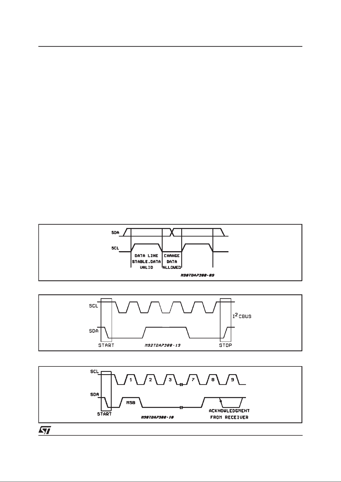
C BUS INTERFACE
I
Data transmission from microprocessor to the
TDA7319 and viceversa takes place thru the 2
wires I
2
C BUS interface, consisting of the two
lines SDA and SCL (pull-up resistors to positive
supply voltage must beexternallyconnected).
Data Validity
As shown in fig. 3, the data on the SDA line must
be stable during the high period of theclock. The
HIGH and LOW state of the data line can only
change when the clock signal on the SCL line is
LOW.
Start and Stop Conditions
As shown in fig.4 a start condition is a HIGH to
LOW transition of the SDA line while SCL is
HIGH. The stop condition is a LOW to HIGH transition of the SDA line while SCLis HIGH.
Byte Format
Every byte transferred to the SDA line must contain 8 bits. Each byte must be followed by an acknowledgebit. The MSB is transferredfirst.
TDA7339
Acknowledge
The master(µP) puts a resistiveHIGHlevelon the
SDA line during the acknowledge clock pulse (see
fig. 5). The peripheral (audioprocessor) that acknowledges has to pull-down (LOW) the SDA line
during the acknowledge clock pulse, so that the
SDAlineisstableLOWduringthisclockpulse.
The audioprocessor which has been addressed
has to generate an acknowledge after the reception of each byte, otherwise the SDA line remains
at the HIGH level during the ninth clock pulse
time. In this case the master transmitter can generate the STOP information in order to abort the
transfer.
Transmissionwithout Acknowledge
Avoiding to detect the acknowledge of the audioprocessor, theµP can use a simplier transmission: simply it generates the 9th clock pulse without checking the slave acknowledging, and then
sendsthe newdata.
This approach of course is less protected from
misworkingand decreasesthe noise immunity.
2
Data Validityon theI
CBUS
Timing Diagram of I2CBUS
2
Acknowledgeon the I
CBUS
5/12

TDA7339
SOFTWARESPECIFICATION
Interface Protocol
The interface protocol comprises:
A start condition (s)
A chip address byte, containing the TDA7339
TDA7339 ADDRESS
MSB
S100001A0
ACK = Acknowledge
S =Start
P =Stop
MAX CLOCK SPEED 100kbits/s
first byte
LSB MSB LSB MSB LSB
ACK DATA ACK DATA ACK P
address(the 8th bit of the bytemust be 0). The
TDA7339must always acknowledgeat theend
of each transmitted byte.
A sequenceof data(N-bytes+ acknowledge)
A stopcondition (P)
Data Transferred (N-bytes+ Acknowledge)
SOFTWARESPECIFICATION
Chip address
1
MSB
A =Logic level ON pin ADDR
00001A0
FUNCTIONCODES
MSB F6 F5 F4 F3 F2 F1 LSB
1st VOLUME 0 F6F5F4F3F2F1 0
2nd VOLUME 0 F6F5F4F3F2F1 1
TREBLE 100F4F3F2F1F0
MIDDLE 101F4F3F2F1F0
BASS
MUTMUX 111F4F3F2F1F0
POWERON RESET:
1st volume = 2nd volume= Mute
Treble = Middle= Bass = -14dB
Mutmux= ActiveInputIN 1
LSB
110F4F3F2F1F0
6/12

1st VOLUMECODES
MSB F6 F5 F4 F3 F2 F1 LSB FUNCTION
0 0 step 1dB
0 0 0 0dB
0 0 1 -1dB
0 1 0 -2dB
0 1 1 -3dB
1 0 0 -4dB
1 0 1 -5dB
1 1 0 -6dB
1 1 1 -7dB
0 0 step 8dB
000 0dB
0 0 1 -8dB
0 1 0 -16dB
0 1 1 -24dB
1 0 0 -32dB
1 0 1 -40dB
1 1 1 MUTE
TDA7339
2nd VOLUMECODES
MSB F6 F5 F4 F3 F2 F1 LSB FUNCTION
0 1 step 1dB
0 0 0 0dB
0 0 1 -1dB
0 1 0 -2dB
0 1 1 -3dB
1 0 0 -4dB
1 0 1 -5dB
1 1 0 -6dB
1 1 1 -7dB
0 1 step 8dB
000 0dB
0 0 1 -8dB
0 1 0 -16dB
0 1 1 -24dB
1 0 0 -32dB
1 0 1 -40dB
1 1 1 MUTE
7/12

TDA7339
TREBLE CODES
MSB F6 F5 F4 F3 F2 F1 LSB FUNCTION
1 0 0 TREBLE BOOST
00000 0dB
00001 1dB
00010 2dB
00011 3dB
00100 4dB
00101 5dB
00110 6dB
00111 7dB
01000 8dB
01001 9dB
0 1 0 1 0 10dB
0 1 0 1 1 11dB
0 1 1 0 0 12dB
0 1 1 0 1 13dB
0 1 1 1 0 14dB
0 1 1 1 1 14dB
1 0 0 TREBLE CUT
10000 0dB
1 0 0 0 1 -1dB
1 0 0 1 0 -2dB
1 0 0 1 1 -3dB
1 0 1 0 0 -4dB
1 0 1 0 1 -5dB
1 0 1 1 0 -6dB
1 0 1 1 1 -7dB
1 1 0 0 0 -8dB
1 1 0 0 1 -9dB
1 1 0 1 0 -10dB
1 1 0 1 1 -11dB
1 1 1 0 0 -12dB
1 1 1 0 1 -13dB
1 1 1 1 0 -14dB
1 1 1 1 1 -14dB
8/12

MIDDLE CODES
MSB F6 F5 F4 F3 F2 F1 LSB FUNCTION
1 0 1 MIDDLE BOOST
00000 0dB
00001 1dB
00010 2dB
00011 3dB
00100 4dB
00101 5dB
00110 6dB
00111 7dB
01000 8dB
01001 9dB
0 1 0 1 0 10dB
0 1 0 1 1 11dB
0 1 1 0 0 12dB
0 1 1 0 1 13dB
0 1 1 1 0 14dB
0 1 1 1 1 14dB
1 0 1 MIDDLE CUT
10000 0dB
1 0 0 0 1 -1dB
1 0 0 1 0 -2dB
1 0 0 1 1 -3dB
1 0 1 0 0 -4dB
1 0 1 0 1 -5dB
1 0 1 1 0 -6dB
1 0 1 1 1 -7dB
1 1 0 0 0 -8dB
1 1 0 0 1 -9dB
1 1 0 1 0 -10dB
1 1 0 1 1 -11dB
1 1 1 0 0 -12dB
1 1 1 0 1 -13dB
1 1 1 1 0 -14dB
1 1 1 1 1 -14dB
TDA7339
9/12
TDA7339
BASS CODES
MSB F6 F5 F4 F3 F2 F1 LSB FUNCTION
1 1 0 BASS BOOST
00000 0dB
00001 1dB
00010 2dB
00011 3dB
00100 4dB
00101 5dB
00110 6dB
00111 7dB
01000 8dB
01001 9dB
0 1 0 1 0 10dB
0 1 0 1 1 11dB
0 1 1 0 0 12dB
0 1 1 0 1 13dB
0 1 1 1 0 14dB
0 1 1 1 1 14dB
1 1 0 BASS CUT
10000 0dB
1 0 0 0 1 -1dB
1 0 0 1 0 -2dB
1 0 0 1 1 -3dB
1 0 1 0 0 -4dB
1 0 1 0 1 -5dB
1 0 1 1 0 -6dB
1 0 1 1 1 -7dB
1 1 0 0 0 -8dB
1 1 0 0 1 -9dB
1 1 0 1 0 -10dB
1 1 0 1 1 -11dB
1 1 1 0 0 -12dB
1 1 1 0 1 -13dB
1 1 1 1 0 -14dB
1 1 1 1 1 -14dB
MUTMUX CODES
MSB F6 F5 F4 F3 F2 F1 LSB FUNCTION
1 1 1 INPUTS
XXX00SLOWSOFTMUTESLOPE(I=I
X X X 0 1 FASTSOFTMUTE SLOPE(I=I
X X X 1 X SOFT MUTE OFF
X 0 0 NOT ALLOWED
X 0 1 IN3
X 1 0 IN2
X 1 1 IN1
10/12
MIN
MAN
)
)

TDA7339
DIM.
MIN. TYP. MAX. MIN. TYP. MAX.
a1 0.63 0.025
b 0.45 0.018
b1 0.23 0.31 0.009
b2 1.27 0.050
D 37.34 1.470
E 15.2 16.68 0.598 0.657
e 2.54 0.100
e3 33.02 1.300
F 14.1 0.555
I 4.445 0.175
L 3.3 0.130
mm inch
0.012
OUTLINE AND
MECHANICAL DATA
DIP28
11/12

TDA7339
Information furnished is believed to be accurate and reliable. However, STMicroelectronics assumes no responsibility for the consequences
of use of such information nor for any infringement of patents or other rights of third parties which may result from its use. No license is
granted by implication or otherwise under any patent or patent rights of STMicroelectronics. Specification mentioned in this publication are
subject to change without notice. This publication supersedes and replaces all information previously supplied. STMicroelectronics products
are not authorized for use ascriticalcomponents in life support devices or systems without express written approvalof STMicroelectronics.
The ST logo is a registeredtrademark of STMicroelectronics
1999 STMicroelectronics – Printed inItaly– AllRights Reserved
STMicroelectronics GROUP OF COMPANIES
Australia - Brazil -China- Finland- France - Germany - Hong Kong - India- Italy - Japan - Malaysia - Malta - Morocco -
Singapore - Spain -Sweden- Switzerland - United Kingdom - U.S.A.
http://www.st.com
12/12
 Loading...