

INTEGRATED 19KHz SC NOTCH FILTER
FOR PILOTCANCELLATION
ON CHIP FILTER FOR PILOT DETECTOR
AND PLL
ADJUSTMENT FREE VOLTAGE CONTROLLED OSCILLATOR
AUTOMATIC PILOT DEPENDENT MONO/
STEREOSWITCHING
NOISE BLANKING WITH PROGRAMMABLE
THRESHOLD
HIGHCUTCONTROL AND STEREO BLEND
INTEGRATED HIGH PASS FILTER FOR IN-
TERFERENCE DETECTOR
LEVEL INPUT FOR ADDITIONAL SPIKE DE-
TECTIONON FIELDSTRENGHTSIGNAL
VERY HIGH SUPPRESSION OF HARMONIC
AND INTERFERENCE SIGNALS
STEREO DECODER
ORDERING NUMBER:
TDA7338
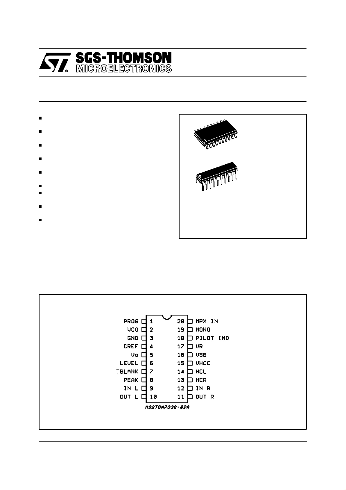
SO20
DIP20
TDA7338(DIP20)
TDA7338D(SO20)
DESCRIPTION
The TDA7338 is a newconcept of monolithicintegrated stereodecoder with noise blanking for FM
car radio applications.
With the used BICMOS technique, the 19KHz
Notch Filter, the PLL Filter and Phase Filter is re-
PIN CONNECTION(Top view)
alized on the chip with a Switched Capacitor concept.
Avoiding the use of multipliers and non linear circuits a very high performance in terms of noise
suppression and total harmonic distortion is
reached.
December 1996
1/11
TDA7338
ABSOLUTE MAXIMUM RATINGS
Symbol Parameter Value Unit
V
CC
I
CC
T
stg
T
amb
THERMAL DATA
Symbol Description DIP 20 SO 20 Unit
R
thj-pins
ESD
All pins are protectedagainst ESD according to the MIL883 standard.
BLOCK DIAGRAM AND TEST CIRCUIT
DC Supply Voltage 10.5 V
Supply Current 20 mA
Storage temperature -55 to 150
Operating ambient temperature -40 to 85 °C
Thermal resistance junction-pins Typ 100 200
°
C/W
°
C
MPX IN
70K
DETECTOR
1µF
40.2K
20 19 18 17 16 15 14 13
AMP
80KHz
LPF
PLL
SC
PHASE
&
PHASE
FILTER
CSB456F11
MPX
PILOT
IND.
MONO
PILOT
DETECTOR
DEMODULATOR
DIVIDERS
VCO
2617835
VCO
VR VSB VHCC
LEVEL
CONTROL
25KHz
LPF
AMP
140KHz
LPF
120KHz
LPF
LEVEL PROG GND V
NOISE
19KHz
SC NOTCH
PEAK
DETECTOR
TRIGGER
THRESHOLD
VCO OFF MUTE
BLANKER
PULSE
FORMER
TBLANK PEAK
1nF 1nF
HCRHCL
HIGH
CUT
CONTROL
47nF470pF
20K
20K
REFERENCE
AMP
AMP
S
D95AU364C
IN R
12
40.2K
11
OUT R
OUT L
10
40.2K
9
IN L
CREF
4
4.7µF
2/11
TDA7338
ELECTRICALCHARACTERISTICS (VCC= 9V;modulation frequency:1KHz;de-emphasistime:
T=50µs; nominal MPX input voltage: V
=40.2kΩ,R
R
IN
Symbol Parameter Test Condition Min. Typ. Max. Unit
V
CC
I
CC
V
IN
V
ORMS
SVRR Supply VoltageRipple Rejection V
V
L/VR
V
o/Vi
R
O
V
O
α Channel Separation V
THD Total Harmonic distortion 0.02 0.3 %
S+N
N
α
M
V
DC
= 40.2kΩ;T
OUT
=27°C; C
amb
Supply Voltage 7.5 9 10.2 V
Supply Current 5 10 15 mA
MPX Input Level (peak to peak) fm= 1KHz 1.5 V
A.F. Output Voltage (mono) pin 10 and 11VIN= 0.5V
DifferenceofOutputVoltageLevels pin 10 and 11- mono -0.8 0.8 dB
Gain V10/V
Output Resistance pin 10 and 11 10 50
DC Output Voltage pin 10 and 11 4.2 4.5 4.8 V
Signal plus noise to noise ratio f= 20Hz to 16KHz;
Muting Attenuation V7and V8< 0.6V 100 dB
Mute DC Steps at pins 10, 11 Mute at pin 8 0 4 mV
CARRIER ANDHARMONIC SUPPRESSIONAT THEOUTPUT
= 1.5VPP; m 100%(75KHz deviation,f
MPX
=4.7µF; unless otherwisespecified)
REF
RMS
MONO;
= 200mV; f = 1KHz 40 55 dB
RIPPLE
20
= -50mV
R-VSB
DC
S = 2Vrms
=1KHz);
mod
1.5 V
8.5 9.5 10.5 dB
30 45 dB
91 dB
Ω
α19 Pilot Signal f = 19KHz 55 70 dB
38 Subcarrier f = 38KHz 75 dB
α
57 Subcarrier f = 57KHz 62 dB
α
α76 Subcarrier f = 76KHz 90 dB
INTERMODULATION(note 1)
2f
α
α3f
= 10KHz; f
mod
= 13KHz; f
mod
= 1KHz 65 dB
spur
= 1KHz 75 dB
spur
TRAFFICRADIO (note 2)
α57 Signal f = 57KHz 70 dB
SCA - SUBSIDIARYCOMMUNICATIONS AUTHORIZATION (note 3)
67 Signal f = 67KHz 75 dB
α
ACI - ADJACENTCHANNEL INTERFERENCE(note4)
114 Signalf = 114KHz 95 dB
α
190 Signalf = 190KHz 84 dB
α
MONO/ STEREO SWITCH
V
V
INTH
INTH
V
I
V
PI
PI
19
Pilot Threshold Voltage for stereo ”ON” 12 20 28 mV
Pilot Threshold Voltage for stereo ”OFF” 7 14 21 mV
Pilot Indicator Saturation Voltage I = 1mA 0.2 0.5 V
Pilot Indicator Leakage Current V = 9V 10
Control Voltage for forced mono α = < 3dB 0.8 V
STEREOBLEND
µ
RMS
RMS
A
V
V
16-17
16-17
Control Voltage for Channel
Separation
Control Voltage for Channel
Separation
= 6dB; VR= 3.6V (note 5) -0.31 -0.27 -0.23 V
α
= 26dB; -85 -55 -30 mV
α
3/11
TDA7338
ELECTRICALCHARACTERISTICS (continued)
HIGH CUT CONTROL
Symbol Parameter Test Condition Min. Typ. Max. Unit
VCO
τ
deemp
R
15-17
R
15-17
De-Emphasis Time Constant C13,C14= 1nF; V
High Cut Control Resistance V
= 50mV 43 50 57 K
15 - 17
High Cut Control Resistance V15 - 17 = -0.5V (note 5) 115 150 185 KΩ
= 50mV 43 50 57
15-17
s
µ
Ω
f
osc
f/f Capture and Holding Range
∆
V
VCO
Oscillator Frequency with Murata CSB456F11 456 KHz
V
CO OFF
Pin 7 0.6 V
NOISE INTERFACEDETECTOR (test condition:VSB>VR+ 50mV)
V
TR
V
TR
T
S
I
OS
V
N1
V
N2
V
N3
Trigger Threshold (note 6) V
Trigger Threshold V
Suppression Pulse Duration C
Input Offset Current during
suppression time
V
(pin 8) VIN= 0mV
PEAK
V
(pin 8) VIN= 50mV
PEAK
V
(pin 8) VIN= 100mV
PEAK
= 1.3V; PROG = GND 180 mV
PEAK
= 1.3V;
V
PEAK
PROG= OPEN/V
= 1.5V; PROG = GND 260 mV
PEAK
= 1.5V;
V
PEAK
PROG= OPEN/V
= 470pF 50
BLANK
DD
DD
RMS
; f = 150KHz 1.1 1.5 2 V
RMS
; f = 150KHz 1.7 2.3 2.8 V
RMS
NOTES TO THE CHARACTERISTICS
1 INTERMODULATIONSUPPRESSION
V
(signal)(at1KHz)
α2 =
O
V
(spurious)(at1KHZ)
O
;f
= (2 x 10KHz) - 19KHz
s
1%
±
250 mV
340 mV
10 pA
0.7 1.0 1.3 V
s
µ
α3 =
O
(spurious)(at1KHZ)
V
O
;f
= (3 x 13KHz) - 38KHz
s
(signal)(at1KHz)
V
measuredwith : 91% mono signal;9% pilot signal; fm=10KHzor 13KHz
2. TRAFFIC RADIO(V.F.) suppression
α57 (V.W.F.)
V
=
VO(spurious) (at1KHZ ±23Hz)
O(signal)
(
at1KHz
)
measuredwith : 91% stereo signal; 9% pilot signal; fm=1KHz; 5% subcarrier
(f=57KHz,fm = 23Hz AM,m = 60%)
3. SCA (SUBSIDIARYCOMMUNICATIONS AUTHORIZATION)
α67
V
O(signal)
=
V
(spurious)(at9KHZ)
O
at
(
1KHz)
;f
= (2x 38KHz) - 67KHz
s
measuredwith : 81% mono signal;9% pilot signal; fm=1KHz;
10% SCA - subcarrier(f
4/11
= 67KHz,unmodulated)
s

NOTES TO THE CHZARACTERISTICS (continued)
4. ACI (ADJACENTCHANNEL INTERFERENCE)
α114 =
α190 =
O
(spurious)(at4KHZ)
V
O
(signal) (at1KHz)
V
O
(spurious)(at
V
O
4
KHZ)
;f
= 110KHz- (3 x 38KHz)
s
;f
= 186KHz- (5 x 38KHz)
s
(signal) (at1KHz)
V
measuredwith : 90% mono signal;9% pilot signal; fm=1KHz; 1% spurioussignal
= 110KHzor 186KHz,unmodulated)
(f
s
R
5. Control range typ 11% of V
(see figure1 and figure2)
6. MEASUREMENTOF TRIGGERTHRESHOLDS
TDA7338
All thresholdsare measured by using a pulse
with T
R
=2µs, T
HIGH
=2µs, andTF=10µs.
The repetitionrate must not increase the PEAK
voltage.
FUNCTIONAL DESCRIPTION
Signal Path
The TDA7338 Stereodecoder contains all necessary functionsfor processingthe MPX signal. Due
to the external input resistance (Pin 20) the circuit
can be adapted to different MPX input levels. Behind a 80kHz lowpass filter the adjustment free
PLL for the pilot Tone is placed.The only external
component needed for the PLL is the ceramic
Figure 1: High Cut Control
f
c
(KHz)
3.18
(=50µs)
2
V
=3.6V
R
D95AU366
V
in
V
TR
DC
D95AU365
TRT
HIGH
T
F
Time
resonatorfor the oscillator whichruns at 456kHz.
The pilot detector output is designed as an open
collector output, therefore an external pullup resistor is needed. To force the decoderto ”MONO”
Pin 19 has to be clamped to a voltage below
0.8V.
The voltagelevel (signal strength fromthe IFpart)
applied to Pin 15 (VHCC) allows to control the
time constant of the deemphasis (nom. = 50µs,
see fig. 1). If the RF-signal is weak, the corner
Figure2: Stereo Blend
SEP
(dB)
50
40
30
V
=3.6V
R
D95AU367
1
0
-0.5 -0.4 -0.3 -0.2 -0.1 0.0 V
HCC-VR
(V)
20
10
0
-0.40 -0.32 -0.24 -0.16 -0.08 VSB-VR(V)
5/11

TDA7338
frequency is reduced down to 1kHz to improve
the signal to noise ratio. Furthermore the conditions of the stereo separation (see fig.2) can be
controlled through the signal applied to Pin 16
(VSB). Both signal levels (VSB and VHCC) are
referred to Pin 17 (VR), with the characteristic
that the control rangeis 11% of V
R.
By modifying the feedback resistor value of the
output stages (Pin 9 - 10, Pin 11 - 12) the total
gain of the stereodecodercan be modified.
Pin 7 and Pin 8 have an additional function. By
pulling them to ground the VCO-OFF (Pin 7) and
the MUTE (Pin 8) function are activated. The
MUTE signal disconnects the MPX-signal from
the circuit, while in combination with VCO-OFF
also the output buffers are disconnected from the
circuit. In this mode the output buffers can be
used for AM-stereo,cassette play back and other
purposes.
AM Mono Mode
By selecting VCO-OFF (Pin 7 to GND) the VCO
is switchedoff and the SB and HCC are disabled.
The deemphasis time constant is changed to
40µs(f
= 4KHz).
c
DESCRIPTIONOF THE NOISE BLANKER
In the normal automotive environment the MPX
signal is disturbed by ignition spikes, motors and
high frequency switches etc.
The aim of the noise blanker part is to cancel the
influence of the spikes producedby these components. Therefore the output of the stereodecoder
is switched off for a time of 40µs (average spike
duration).
In a first stage the spikes must be detectedbut to
avoid a wrong triggering on high frequency noise
a complextrigger control isimplemented.
Behind the trigger stage a pulse former generates
the40µs ”blanking”pulse.
This duration of 40µs can be varied by changing
the capacitorat pin 7.
1.1 Trigger Path
The incoming MPX signal is highpass-filtered,
amplifiedand rectified(block RECT-PEAK).
The second order highpass-filterhas a corner-frequency of 140KHz.
The rectifier signal, RECT, is used to generate by
peak-rectification a signal called PEAK, which is
available at the PEAKpin 8.
Also noise with a frequency >100KHz increases
the PEAK voltage. The value of the PEAK voltage
influences the trigger threshold voltage Vth (block
ATC). The higher the noise level the higher the
threshold.
Both signals, RECT and PEAK+Vth are fed to a
comparator (block PEAK-COMP) which outputs a
sawtooth-shapedwaveform at the TBLANK pin 7.
A second comparator (block BLANK-COMP)
formsthe internal blankingduration of 40µs.
The noise blanker is supplied by his own biasing
circuit (block BIAS-MONO)to avoid any crosstalk
to the signalpath (blockBIAS-MONO).
1.2 Noise Controlled ThresholdAdjustment
(ATC)
The behaviour of the noise controlled threshold
adjustmentis shown in fig. 4. It can be influenced
slightly by adding a resistor in parallel to the
PEAK capacitor at Pin 8 either to GND or V
DD.A
resistor to GND will decrease the threshold
DD
whereas a resistor to V
will increase it. But it is
recommended to choose one of the internal
thresholdsby use of the PROG pin (see table1)
1.3 AutomaticThreshold Control by the
Stereoblendvoltage (ATC-SB)
Besides the noise controlled thresholdadjustment
there is an additional possibilityfor influencingthe
trigger. It is controlled by the difference between
Vsb and Vr, similar to the Stereoblend. The reason for implementing such a second control will
be explainedin the following:
The point where the MPX signal starts to become
noisy is fixed by the RF part. Therefore also the
starting point of the normal noise controlled trigger adjustment is fixed (fig.5). But in some cases
the behaviour of the noiseblanker can be improved by increasing the threshold even in a region of higher fieldstrength, for the MPX signal
often shows distortion in this range, which leads
to an undesiredtriggering.
Because of the overlap of this range and the
range of the stereo/mono transition it can be controlled by Vsb and Vr. This threshold increase is
programmable(seefig.5).
1.4 BlendMode
Another possibility to avoid a disturbing triggering
on modulation is to use the spikes on the fieldstrength signal (LEVEL pin). But in the range of
higher fieldstrength the signal saturates and no
more spike detection is possible. For this reason
the TDA7338 offers the ”BLEND MODE”. When
”BLEND MODE” is activated a smooth transition
between the LEVEL- and the MPX-signal is used
to detect the spikeseither on LEVELor on MPX.
In the lower fieldstrength range mainly the
LEVEL-signal is used whereas in the higher
range mainly the MPX is used. This switching is
controlled also by the normal Stereoblend signal
to avoid additionalpins.
”BLEND MODE OFF” is activated by connecting
the LEVEL pin to GND (LEVEL must be also connectedto GND if notused).
6/11

Figure 3: BlockDiagram of the Noise Blanker
TDA7338
MPX IN
LEVEL
BLEND
ON/OFF
V
R
V
SB
0.1V
80KHz LP
140KHz HP
120KHz HP
BLEND
CONTROL
ADDITIONAL
+
-
THRESHOLD
CONTROL
(ATC-SB)
D95AU368
SIGNAL PATH
AMP
Table 1: Programmingof the Noiseblanker
PIN 1 (PROG) Trigger Threshold Peak Voltage Control By Fieldstrength
GND LOW ON
OPEN HIGH ON
V
DD
HIGH OFF
BUF
RECT-PEAK
RECT
PEAK
AUTOMATIC
THRESHOLD
CONTROL
ADDITIONAL
C
PEAK
47nF
PEAK COMP
-
+
PEAK+VTH
ATC
THRESHOLD L/H
THRESHOLD
CONTROL on/off
C
BLANK
330pF
BLANK COMP
REF.
-
+
LEFT
RIGHT
40µs
to OUTPUTS
2V
V
S
PROG
7V
Figure 4: TriggerThreshold vs. V
VTH
100mV
60mV
PEAK
MIN. TRIG. THRESHOLD
0.9V
D95AU369
300mV
180mV
ADJUSTED
NOISE
TRIG. THRESHOLD
1.5V
V
PEAK(V)
7/11

TDA7338
Figure 5: Behaviourof the Field StrengthControlledThreshold Adiustment
V
PEAK
MONO STEREO
≈3V
TRIG. THRESHOLD
NOISE
noisy signal good signal
Figure 6: ApplicationDiagram
SIGNAL
STRENGTH
VR 17
PILOT_IND 18
MONO
MPX
VCO_OFF
(FM ENABLE)
68K 1)
47K
47K 1)
100K
68K
470nF
33K
100K
100K
1) has to be adapted to the signal strength
2) for deemphasis = 50µs
3) not absolutely necessary
4) roll off: to be adjusted to the tuner part
10K
680pF
330pF
47K
4)
15
16
19
20
7
456KHz
D95AU370
24
1
TDA7338
9V
V
S
ATC_SB OFF
(PROG=VS)
35
100nF10µF
2.2V
0.9V
E’
1nF 2)
14
13
1nF 2)
12
47K
11
6 LEVEL
9
47K
10
8
47nF
IN R
56pF 3)
OUT
(SIGNAL STRENGTH)
IN L
56pF 3)
OUT
10K
10K
D95AU371A
MUTE
8/11

SO20 PACKAGEMECHANICAL DATA
TDA7338
DIM.
MIN. TYP. MAX. MIN. TYP. MAX.
A 2.65 0.104
a1 0.1 0.3 0.004 0.012
a2 2.45 0.096
b 0.35 0.49 0.014 0.019
b1 0.23 0.32 0.009 0.013
C 0.5 0.020
c1 45 (typ.)
D 12.6 13.0 0.496 0.512
E 10 10.65 0.394 0.419
e 1.27 0.050
e3 11.43 0.450
F 7.4 7.6 0.291 0.299
L 0.5 1.27 0.020 0.050
M 0.75 0.030
S 8 (max.)
mm inch
9/11

TDA7338
DIP20 PACKAGEMECHANICAL DATA
DIM.
MIN. TYP. MAX. MIN. TYP. MAX.
a1 0.254 0.010
B 1.39 1.65 0.055 0.065
b 0.45 0.018
b1 0.25 0.010
D 25.4 1.000
E 8.5 0.335
e 2.54 0.100
e3 22.86 0.900
F 7.1 0.280
I 3.93 0.155
L 3.3 0.130
Z 1.34 0.053
mm inch
10/11

TDA7338
Information furnished is believed to be accurate and reliable. However, SGS-THOMSON Microelectronics assumes no responsibility for the
consequences of use of such information nor for any infringement of patents or other rights of third parties which may result from its use. No
license is granted by implicationor otherwise under any patent or patentrights of SGS-THOMSON Microelectronics. Specification mentioned
in this publication are subject to change without notice. This publication supersedes and replaces all information previously supplied. SGSTHOMSON Microelectronics products are not authorized for use as critical components in life support devices or systems without express
written approval of SGS-THOMSON Microelectronics.
1996 SGS-THOMSON Microelectronics – Printed in Italy – All Rights Reserved
Australia - Brazil - Canada - China - France - Germany - Hong Kong - Italy- Japan - Korea - Malaysia - Malta - Morocco - The Netherlands -
Singapore - Spain - Sweden - Switzerland- Taiwan - Thailand - United Kingdom - U.S.A.
SGS-THOMSON Microelectronics GROUP OF COMPANIES
11/11
 Loading...