

TDA7336
STEREO PREAMP + AMS + DOLBY B*
NOISE REDUCTIONPROCESSOR
DUAL CHANNEL PROCESSOR FOR PLAYBACK APPLICATIONS.
STEREODOLBYB NR SYSTEM
LOW NOISE HEAD PREAMPLIFIER
MUTE, AMS (AUDIO MUSIC SENSOR)
FUNCTIONS
INTERNALSWITCHES FOR EQUALIZATION
DOLBY REFERENCE LEVEL -6dBm
(388.2mV
RMS)
MINIMUM NUMBER OF EXTERNALCOMPONENTS
LOW SUPPLY CURRENT(18mA)
MIXED BIPOLAR/CMOSTECHNOLOGY
DESCRIPTION
The TDA7336 is a monolithic BICmos IC designed for use in stereo cassette player systems.
The device includes two separate audio channels
composed by low noise preamplifier, Dolby B
noise reduction system and Audio Music Sensor.
The dual preamplifier contains mute, metal/normal facilities for amplification of low level signal in
applications requiring very low noise performances.
Each channel consists of two cascaded operational amplifiers.
The first one, AMP1, has a fixed gain of 36dB,
and allows magnetic heads connection directly to
ground. The secondone, AMP2, is a standard operational amplifier whose equalizing external
componentsfix the frequencyresponse.
The Audio Music Sensor circuit detects the interprogram space and then the starting point of musical programs (the interprogram time and program detectiontime are externallyselectable).
The device contains Dolby B decoder NR chains
requiring very few external components and do
not require coils.
* Dolby B and the Double-D symbol are
trademarks of Dolby Laboratories Licensing Corporation, San Francisco,
California94103-4813,USA.
This device is available only to Licensing and application information may be
obtainedfrom Dolby Lab.
November 1999
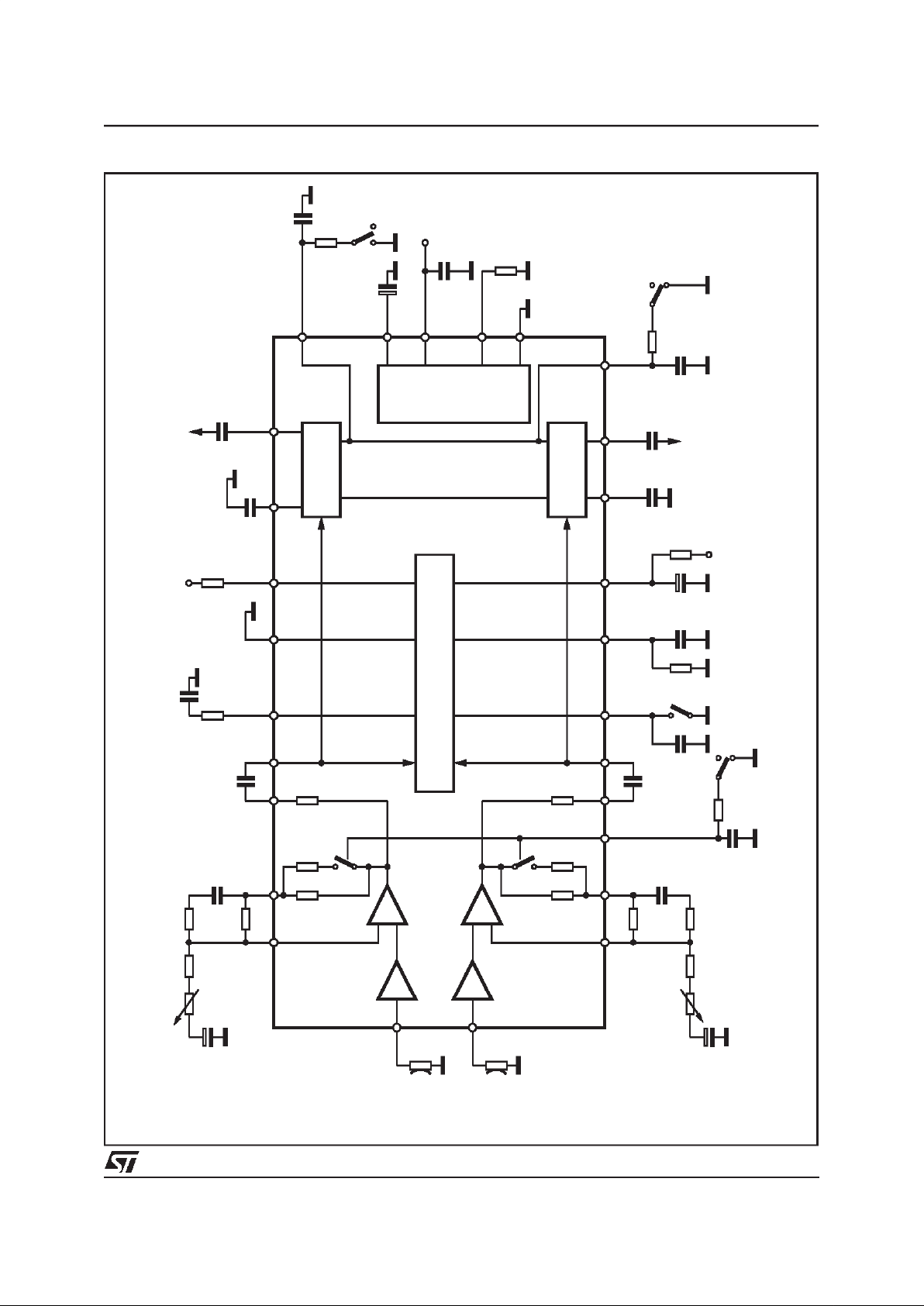
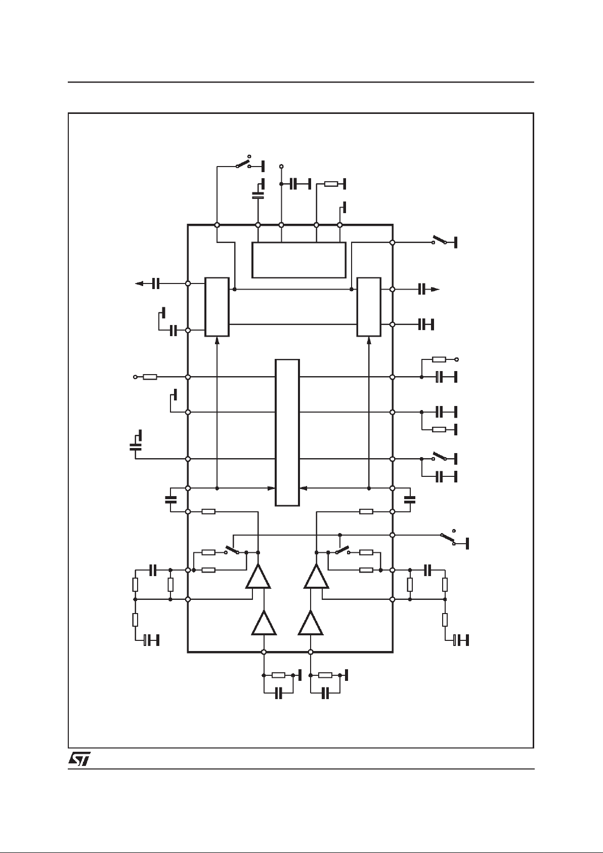
DINL
AMS SW
INTP
INTS
MUTE
DOUTL
TCL
IREF
N.C.
1
3
2
4
5
6
7
8
9
Vs
VREF
DOUTR
NR SW
TCR
AMSGin
AMSOUT
GND DIG
DINR23
22
21
20
19
17
18
16
15
D94AU052
10
11
12
13
14
28
27
26
25
24
GND
INL
EQLI
EQLO
OUTL OUTR
EQRO
EQRI
INR
EQ.SW
PIN CONNECTION
(Top view)
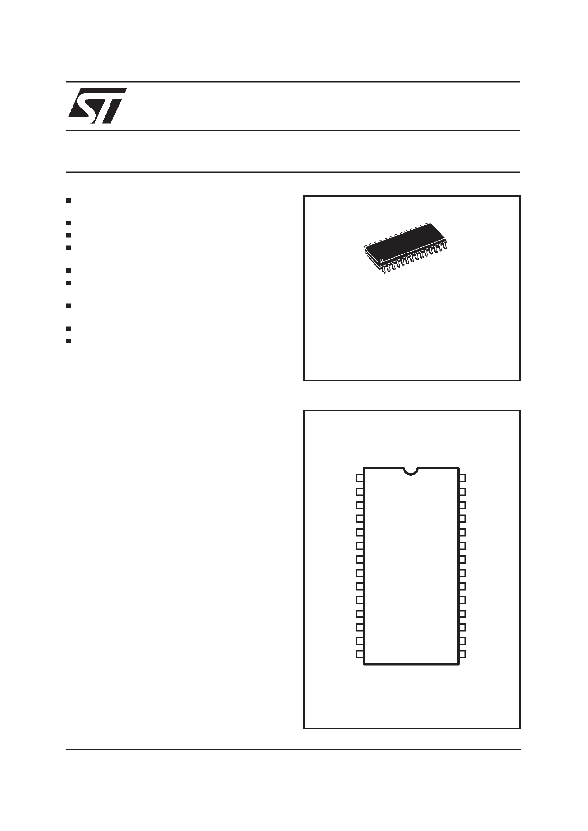
SO28
ORDERING NUMBER: TDA7336
1/20
ABSOLUTE MAXIMUM RATINGS
Symbol Parameter Value Unit
V
S
Supply Voltage 12 V
P
tot Total Power Dissipation 1 W
T
op
Operating Temperature Range -40 to 85
°
C
T
stg
Storage Temperature Range -40 to 150
°
C
THERMAL DATA
Rth j-pins Thermal resistance junction-pins 85 °C/W
PIN FUNCTIONS
N. Name VDC (V) Function
1 GND Ground
2 IN L 0 Preamplifier Left Input
3,26 EQLI, EQRI 4.6 Equalizer Inputs
4, 25 EQLO, EQRO 4.6 Equalizer Outputs
5, 24 OUTL, OUTR 4.6 Preamplifier Outputs
6, 23 DINL, DINR V
ref
Dolby NR Inputs
7 AMS SW 5.6 Audio Music Sensor Switch (ON/OFF) HIGH = ON
8 INTP Interprogram Time Constant (”Signal Detection”)
9 INTS Interspace Time Constant (”Blank Detection”)
10 MUTE Mute Switch ON = LOW (2)
11, 18 TLC, TCR 0.4 Dolby Time Constants
12, 17 DOUTL, DOUTR V
ref
Dolby Outputs
13 I
ref
1.2 Reference Current Source
15 V
S Positive Power Supply
16 V
ref V
S
/2 Reference Voltage
19 NR SW Noise reduction ON/OFF: HIGH =OFF (2)
20 AMS GIN 1.4 Audio Music Sensor Input Pin
21 AMS OUT Audio Music SensorOutput Pin (open collector configuration, see Fig. 2)
22 GND DIG. 0 Digital Ground
27 IN R 0 Preamplifier Right Input
28 EQ SW 0 Equalizer Switch (Low = normal position High = metal position)
(2) Internal pull-up resistor (digital high level if pin left open)
TDA7336
2/20
AMS
10nF
C4
6.8K
R5
300K
R6
1.2K
R2
1K
TR2
1µ
F
C2
0.33µF C6(*)
EQRI EQRO OUTR
26 25
RM RN
36dB
AMP1 AMP2
27INR
INPUT R
DINR
24 23
0.22µFC8
R8
10K
AMSGin
20 22
AMSGout
21
R10
100K
Vs
DOLBY
18
TCR
0.68µF(*)C11
DOUTR
OUTR
4.7µ
F
C13
BIAS
4.7µF C14
R13
100K
0.22µF C18
R11
43K
Vs
GND
Vs
0.68µF C19
NRSW
Vs
17
19
16
15
13
1
RNRM
AMP1 AMP2
36dB
2
INPUT L
INL
1.2K
1.2K
3 4 28 5
300K
R4
6.8K
R3
1.2K
R1
1K
TR1
1µ
F
C1
10nF
C3
EQLI EQLO
DOLBY
0.33µF C5(*)
30K
0.68µ
F
C20
Vs
GND
OUTL
DINL
6
100nF C15
AMSSW
7
470K
R7
C7
8
INTP
0.1µF
11
C9
1µF
Vs
100K
R9
TCL
9
INTS
0.68µ
F
(*)
12
DOUTL
C12
4.7µF
OUTL
GND
IREF
VREF
Vs
GND
30K
R15
C16
100nF
D93AU049A
10
MUTE
EQ SW
C10
(*) Capacitor tolerance is ±10%
R14
Figure 1: ApplicationCircuit
TDA7336
3/20
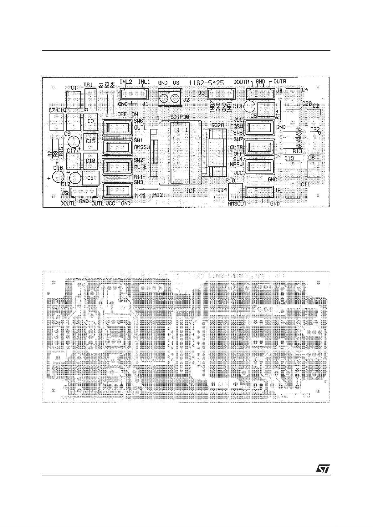
Figure 1a: Components& Top Copper Layer of the Fig. 1 (1:1 scale).
Figure 1b:
Bottom Copper Layer of the Fig. 1 (1:1 scale).
TDA7336
4/20
AMS
10nF
C4
6.8K
R5
300K
R6
1.8K
R2
1µ
F
C2
0.33µF C6(*)
EQRI EQRO OUTR
26 25
RM RN
36dB
AMP1 AMP2
27INR
INPUT R
DINR
24 23
0.22µFC8
R8
10K
AMSGin
20 22
AMSGout
21
R10
100K
Vs
DOLBY
18
TCR
0.68µF(*)
C11
DOUTR
OUTR
4.7µ
F
C13
BIAS
4.7µF C14
0.22µF C18
R11
43K
Vs
GND
Vs
NRSW
Vs
17
19
16
15
13
1
RNRM
AMP1 AMP2
36dB
2
INPUT L
INL
1.2K
1.2K
3 4 28 5
300K
R4
6.8K
R3
1.8K
R1
1µ
F
C1
10nF
C3
EQLI EQLO
DOLBY
0.33µF C5(*)
VsGND
OUTL
DINL
6
100nF C15
AMSSW
7
470K
R7
C7
8
INTP
0.1µF
11
C9
1µF
Vs
100K
R9
TCL
9
INTS
0.68µ
F
(*)
12
DOUTL
C12
4.7µF
OUTL
GND
IREF
VREF
D93AU050A
10
MUTE
EQ SW
600
600300pF
300pF
C10
(*) Capacitor tolerance is ±10%
TEST CIRCUIT
TDA7336
5/20
ELECTRICAL CHARACTERISTICS (VS =8.5V;f=1KHz;Rg=600ΩT
amb
=25°C; R11 = 43KΩ
all level referenced to -6dBm/400Hz, at D
out with NR SW OFF; unle ss o t herwise sp ecif ied
see a pplicat ion circuit of Fig. 1) NAB METAL po sition .
SUPPLY
Symbol Parameter Test Condition Min. Typ. Max. Unit
V
S
Supply Voltage 8 8.5 10.5 V
I
S
Supply Current 11 18 26 mA
V
ref
Reference Voltage (pin 16) 4 4.3 4.6 V
V
DC DC Voltage pin 13 (R
11
= 43K) 1.15 1.25 1.35 V
SVR Ripple Rejection
(Input Referred)
V
ripple
=0.3Vrms DolbyOFF
f
ripple
=1KHz DolbyON
80
85
90
95
dB
dB
MUTE
th
Mute Threshold
Pin 10
ON
OFF
0
2.0
0.8
V
S
V
V
I
MUTE
Mute Current 10 20
µ
A
MUTE
A
Mute Attenuation 55 65 dB
PREAMPLIFIER
R
I
Input Resistance (pin 2, 27) 30 50 70 K
Ω
I
I
Input Bias Current 10
µ
A
G
V Closed Loop Gain pin 3, 4 and 25, 26 shorted 32.5 35.5 38.5 dB
∆G
V Closed Loop Gain Match -1 1 dB
R
M
Resistance Metal Position 4.35 5.8 7.25 K
Ω
R
N
Resistance Normal Position 50 160 300
Ω
e
N
Total Input Noise Unw.B=20Hzto20KHz Rg=0Ω;
R
g =600Ω;
A weighted R
g
=600Ω;
0.45
0.8
0.5
µ
V
µV
µ
V
R
O
Output Impedance (Pin 5, 24) 0.9 1.2 1.7 K
Ω
EQ
l
Normal Low Level (pin 28) 0 1.5 V
EQ
h Metal High Level (pin28) 3.5 VS V
∆R
M
Metal Resistance Matching –2 0 +2 %
AUDIO MUSIC SENSOR
IAMSOUT AMS Output Current 5 mA
VAMS
OUT
AMS Output Low Level IAM
OUT
= 2mA 200 800 mV
R
P
20 Input Impedance 0.8 1.1 1.4 K
Ω
AMS
swl
AMS OFF Low Level 0 0.8 V
AMS
swh AMS ON High Level 2 VS V
V
TH1 Interprogram Threshold Voltage (pin8) 1.2 1.45 1.7 V
VTH
2
Interspace Threshold Voltage (pin 9) 4 4.3 4.6 V
AMS
th
AMS Threshold Level see note (3) 0.6 1 1.4 V
IAMS
sw
AMS Switch pin Current 5 10 15
µ
A
DOLBY SECTION
GV Voltage Gain f = 1KHz; OFF -1 0 1 dB
∆G
V Gain Matching OFF -0.5 0.5 dB
RD
I
Dolby Input Res. (pin 6, 23) 46 63 K
Ω
S/H Signal Handling V
S
= 8V; THD = 1% OFF 12 13 dB
R
DO
Dolby Output Imp. (pin 12, 17) 100 200 300
Ω
B DEC 1 Decode Out f = 10KHz;V
I = 0.4dB ON -1.5 0 1.5 dB
TDA7336
6/20

ELECTRICALCHARACTERISTICS(continued)
DOLBY SECTION
Symbol Parameter Test Condition DOLBY Min. Typ. Max. Unit
B DEC 2 Decode Out f = 500Hz;V
I = -22.1dB ON -26.5 -25 -23.5 dB
B DEC 3 Decode Out f = 2KHz;V
I = -18dB ON -26.5 -25 -23.5 dB
B DEC 4 Decode Out f = 5KHz;V
I
= -29.7dB ON -41.5 -40 -38.5 dB
B DEC 5 Decode Out f = 10KHz;V
I
= -29.6dB ON -41.5 -40 -38.5 dB
NR
l
Dolby ON LowLevel Pin19 0 0.8 V
NR
h Dolby OFF High Level Pin19 2 VS V
GENERAL (PREAMPLIFIER+ DOLBY)
Symbol Parameter Test Condition Min. Typ. Max. Unit
THD Total Harmonic Dist. V
O = 0dB; f = 1KHz Dolby OFF 0.02 0.1 %
V
O
= 0dB; f = 1KHz Dolby ON 0.05 0.1 %
V
O
= 0dB; f = 10KHz Dolby OFF 0.03 %
V
O
= 0dB; f = 10KHz Dolby ON 0.08 %
S/N Signal to Noise Ratio R
g = 600Ω;VO= 0dB;
Unweighted; Dolby OFF
63 dB
R
g
= 600Ω;VO= 0dB;
Unweighted; Dolby ON
70 dB
R
g =600Ω;VO = 0dB;
CCIR/ARM; Dolby OFF
54 63 dB
R
g
=600Ω;VO= 0dB;
CCIR/ARM; Dolby ON
56 72 dB
C
S
Channel Separation Rg = 600Ω; f = 1KHz Dolby OFF 50 64 dB
R
g
= 600Ω; f = 1KHz Dolby ON 70 dB
C
T
Channel Cross Talk Rg= 600Ω; f = 1KHz Dolby OFF 56 70 dB
R
g
= 600Ω; f = 1KHz Dolby ON 75 dB
AMS Gin
RB
0.22µ
F
C8
IN-L
20
1K 100K
Rp20 R9
+
Vs
6
23
IN-R
LIMITER
AMPLIFIER
Vth0
-
+
SIGNAL DETECT.
COMPARATOR
Vs
POWER-ON
RESET
AMS th
NOR1
Q1 Vth1
-
+
21
AMS OUT
Q
FF2
S
R
+
COMP1
COMP2
Vth2
Q2
Q
FF1
R
SQ
0.1µ
F
C7
R7
500K
PROGRAM
DETECTION TIME
T2
T1C15 C9
R9
SPACE
DETECTION
TIME
Vs
INTSAMS SW
INTP
22
8
D93AU051A
97
Figure 2:
AudioMusic Sensor
TDA7336
7/20

AUDIO MUSIC SENSOR (See Figure2)
Aim of this section is to detect interprogram
spaces present on a recordedtape.
Both the blanks (interprogram spaces) and the
programs minimum detectable durations can be
easily set by means of 2 external and independent time constants.
Also the minimum detectable input signal level
can be externally adjusted, by a dedicated gain
network.
Main blocks are:
Variablegain limiter amplifier
Signal detector circuitry
Logicblocksableto avoidunproperoperations.
Operations Description (refer to the simplified
schematic ofFigure 2).
a)The two channels left and right mean signal
coming from the preamp chain (AC coupled)
are added (current)at the AMSinput and presented to the limiter amplifier. The limiter amplifier gain is internally fixed to 40dB, and it
could be reduced by the R8 external resistor.
The AMSVth threshold is fixed at 1V. The following signal detector comparator informs of
the presence of music signal (High level out)
and avoids the erroneous detection of very
lowsignal (like noise) as real program.
b)The system moves in blank detection mode
everytime the supply is turned on or, with
power supplied, the AMS On/Off pin (to be
driven by an open collector output) is turned
off (T
1 open). Once this condition has hap-
pened, the capacitor C
15 charges, defining a
minimum reset time, long enough to reset the
Flip-FlopsFF
1 and FF2 and to descharge the
program detector external C
7 capacitor. The
charging current at the AMS SW pin is about
10µA. It follows that the reset time (C
15 x
V
pin7
)/I
C15
is given approximately by 0.122
x
C15 ns where C15 is in µF.
c)From now on where the sum input signal (left-
right) amplified by the limiter exceeds the sig-
nal detector threshold (3) the capacitor C
7
is
forced to charge. When the voltage across
this capacitor reaches the comparator
COMP
1
thresholdvoltage V
th1
(approx.2 Vbe)
FF
1 is set and FF2 is reset. (4) It follows that
Q
1 is turned on discharging the program de-
tectioncapacitor(C
7).
d)Alwayswhen thereis a recorded zone, Q
1
is
on; it becomes off only if a blank section is
reached. When, with a time constant controlled by the R
9,C9 network the voltage at
space detection time pin reaches V
th2
thresh-
old (comparator COMP
2) a true blank section
is detected and the FF
2 is set. (The minimum
chargingtime is approximatelygiven by:
0.69
x C9xR9[sec]
In this conditionQ
2
ison, forcingthe open collector AMS output to go low, informing the
user that a true blank section has been detected. The state is thenable to start from the
above point c). Figures 3-4 show the signal
behaviour.
The device is able to prevent false interspace detection and the end of thetape. (see Fig. 4).
Note:
(3):minimum RMS input signal is given by:
V
in
= AMSVth ⋅
1K + R
8
101K + R
8
⋅ 0.6
whereV
in
is the mean of left and right channels::
V
in
=
V
right
+ V
left
2
(4): the charging current at pin 8 is about 20µA
(half input signal) so program detection time
constantis given by:
C
7
x
2V
be
20µA
= 70xC
7
[µF] = [msec]
It is recommended to insert a resistor (R7) high
enoughto prevent fast C7 capacitor discharging.
TDA7336
8/20

Figure 4
Figure 3: AMS Timing Diagram
TDA7336
9/20

PINS DESCRIPTION
: Internal Configuration
ELECTRICALCOMPONENTDESCRIPTION(seefigure 1)
COMPONENT
RECOMMENDED
VALUE
PURPOSE
P
R
E
A
M
P
TR
1
,TR
2
C1,C
2
C3,C4
R1,R
2
R3,R
5
R4,R6
1K
Ω
1µF
10nF
1.2K
Ω
6.8K
Ω
300KΩ
Left/Right Channel IN/OUT equalizer filter
TR fixes thegain
150msec NORMAL
70µsec METAL
C
5,C6
0.33µF±10% Preamplifier out to Dolby B input coupling capacitor
A
M
S
R
8
C
8
10K
Ω
0.22µF
Define the AMS input threshold level
V
in
⋅
101K + R
8
1K + R
8
⋅ 1.5> 1V
where V
in
=(V
right+Vleft
)/2
R
7
C7
470KΩ
0.1µF
Set the interprogram detection time:
INTP = 70
x 10
-3
x
C7[µF] = [sec]
R
9
C
9
100K
Ω
1µF
Set the interspace detection time:
INTS = 0.69
xC9xR9
sec
C
15 100nF It fixes music search reset time;
Tres = 0.122
x C15[µF] = [sec] if C15 expressed in µF
D
O
L
B
Y
C
10,C11
0.68µF±10% Dolby output coupling capacitors
C
12,C13
4.7µF±10% Dolby time constants
C
14
4.7µF Reference voltage external capacitor
R
11 43KΩ It fixes the I
ref
current
C
16
R
16
0.1µF
30K
Ω
If fixes the mute time (typ 10msec).
Figure 5: PINS: 2 - 27
Figure6: PINS:6 - 23
TDA7336
10/20

PINS DESCRIPTION: InternalConfiguration
Figure 9: PINS: 3 - 26
Figure12: PINS: 7
Figure 11: PINS: 5 - 24
Figure10: PINS: 4 - 25
Figure 7: PINS: 12 - 17
Figure8: PIN:8
TDA7336
11/20

PINS DESCRIPTION: InternalConfiguration
Figure 15: PIN: 9
Figure18: PIN: 28
Figure 17: PIN: 20
Figure16: PIN: 21
Figure 13: PINS: 11 - 18
Figure14: PIN: 13
TDA7336
12/20

Figure20: PIN: 16
Figure 19: PIN: 19 - 10
Figure22:
QuiescentCurrent vs. Temperature
Figure 21: QuiescentCurrent vs. Supply Voltage
Figure24: THDvs Frequency
Figure 23:
THDvs Supply Voltage
DEVICECHARACTERISTICS
PINS DESCRIPTION: InternalConfiguration
TDA7336
13/20

Figure28: CrossTalk vs. Frequency
Figure 27:
ChannelSeparationvs. Frequency
Figure30: Ripple Rejection vs. Frequency
Figure 29:
RippleRejection vs. Frequency
Figure26:
THD+Nvs. Frequency
Figure 25:
THDvs. Output Signal
DEVICECHARACTERISTICS (continued)
TDA7336
14/20

DEVICECHARACTERISTICS (continued)
Figure34: V
ref&Iref
vsSupply Voltage
Figure 33:
MuteThreshold
Figure36: D.C.Voltagepin 13 vs. SupplyVoltage
Figure 35:
V
ref&Iref
vs Temperature
Figure32:
MuteAttenuationvs. Frequency
Figure 31: Ripple Rejectionvs. Frequency
TDA7336
15/20

DEVICECHARACTERISTICS (continued)
Figure40: Load Characteristics
Figure 39:
NABNetwork
Figure42: SignalHandling vs. Temperature
Figure 41:
SignalingHandling vs.Supply Voltage
Figure38:
NoiseReduction Threshold
Figure 37: EqualizerThreshold
Normal
Metal
TDA7336
16/20

Figure46: AMSInterprogram vs. C7
Figure 45:
AMSReset Time vs. C
ex
Figure48: Interspacevs. C9
Figure 47:
InterprogramCharging Current
Figure44: AMSThreshold vs. Rex
Figure 43: AMS Thresholdvs. Frequency
DEVICECHARACTERISTICS (continued)
TDA7336
17/20

Figure 49: Dolby-BTable
DEVICECHARACTERISTICS (continued)
TDA7336
18/20
SO28
DIM.
mm inch
MIN. TYP. MAX. MIN. TYP. MAX.
A 2.65 0.104
a1 0.1 0.3 0.004 0.012
b 0.35 0.49 0.014 0.019
b1 0.23 0.32 0.009 0.013
C 0.5 0.020
c1 45° (typ.)
D 17.7 18.1 0.697 0.713
E 10 10.65 0.394 0.419
e 1.27 0.050
e3 16.51 0.65
F 7.4 7.6 0.291 0.299
L 0.4 1.27 0.016 0.050
S8°(max.)
OUTLINE AND
MECHANICAL DATA
TDA7336
19/20

Information furnished is believed to be accurate and reliable. However, STMicroelectronics assumes no responsibility for the consequences
of use of such information nor for any infringement of patents or other rights of third parties which may result from its use. No license is
granted by implication or otherwise under any patent or patent rights of STMicroelectronics. Specification mentioned in this publication are
subject to change without notice. This publication supersedes and replaces all information previously supplied. STMicroelectronics products
are not authorized for use as critical components in life support devices or systems without express written approval of STMicroelectronics.
The ST logo is a registered trademark of STMicroelectronics
1999 STMicroelectronics – Printed in Italy – All Rights Reserved
STMicroelectronics GROUP OF COMPANIES
Australia - Brazil - China - Finland - France - Germany - HongKong - India - Italy - Japan - Malaysia - Malta - Morocco -
Singapore - Spain - Sweden - Switzerland - United Kingdom - U.S.A.
http://www.st.com
TDA7336
20/20
 Loading...