

LOW NOISE STEREO PREAMPLIFIER
DUAL CHANNEL PROCESSOR FOR PLAYBACK APPLICATIONS.
LOW NOISE HEAD PREAMPLIFIER
GROUNDCOMPATIBLE
MUTE, AUTOREVERSE METAL/NORMAL
FUNCTIONS
INTERNALSWITCHESFOR EQUALIZATION
LOW SUPPLY CURRENT
MIXED BIPOLAR/CMOSTECHNOLOGY
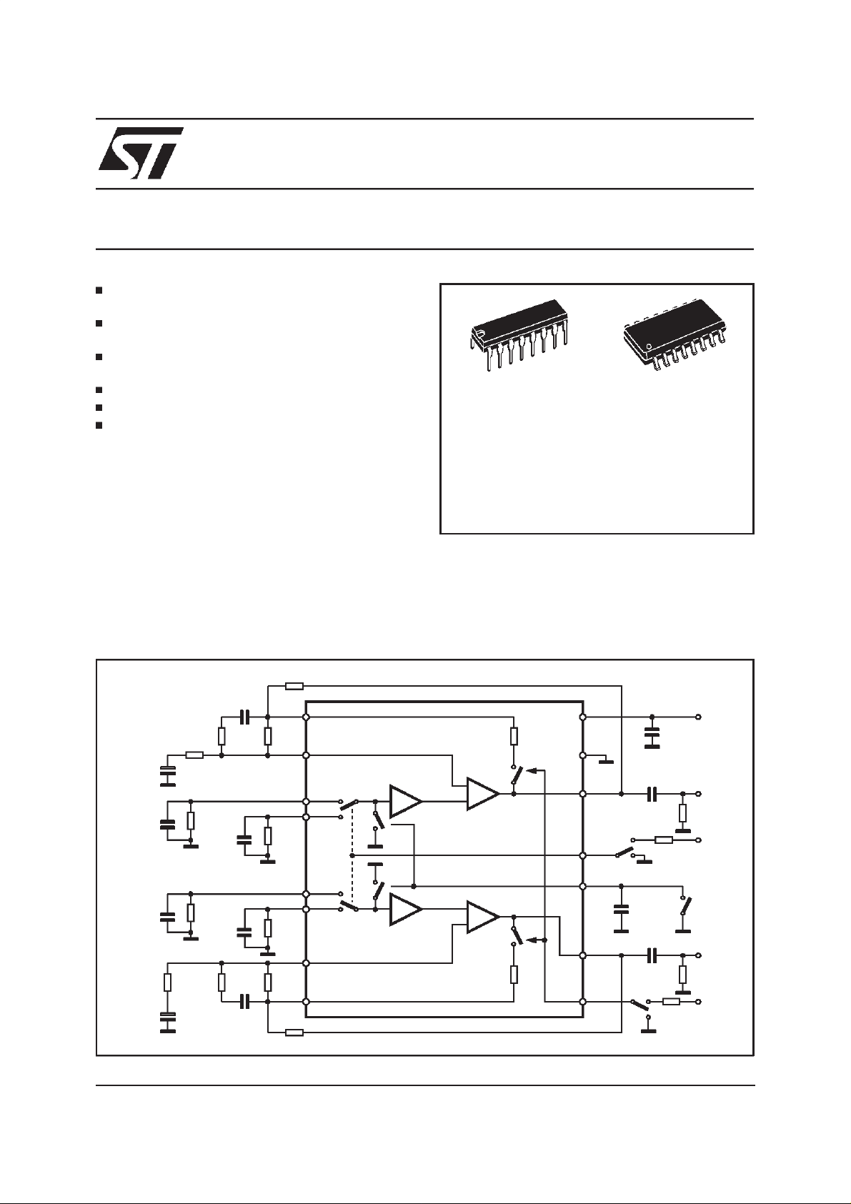
DESCRIPTION
The TDA7334 is a monolithic BICmos IC designed for use in stereo cassette playersystems.
The dual preamplifier contains mute, autoreverse,
metal/normalfacilities for amplification of lowlevel
signal in applications requiringvery low noise performance.
Each channel consists of two cascaded operational amplifiers.
The first one, AMP1, has a fixed gain of 32dB,
TDA7334
DIP16 SO16
ORDERING NUMBER:
low noise forward/reverse switchable input, and
allows magnetic heads connection directly to
ground.The second one, AMP2, is a standard operational amplifier whose equalizing external
componentsfix the frequencyresponse.
TDA7334 (DIP16)
TDA7334D (SO16)
TEST CIRCUIT
R11 1.2K
C11
1µF
INPUT R
C6
300pF
INPUT L
C3
300pF
R3
1.2K
C1
1µF
R10
600Ω
R1
600Ω
R4
6.8K
C5
300pF
C2
300pF
C4 10nF
R13
6.8K
R5
300K
C8 10nF
R15 6.2K
EQRO
R12
300K
EQRI
INR2
INR1
R9
600Ω
INL1
INL223
R2
600Ω
EQLI
EQLO
R14 6.2K
12
RN
13
32dB
14
15
4
5
32dB
AMP1
AMP1
AMP2
AMP2
RN
D94AU079
V
9
GND
1
11
OUTR
F/RSW
8
7 MUTE
OUTL
6
EQSW
16
S
C13 0.22µF
R7 10K
C9
100nF
C14 0.22µF
GND
C12
100nF
R8 10K
20K
20K
+V
S
+V
S
+V
S
November 1999
1/11

TDA7334
ABSOLUTE MAXIMUM RATINGS
Symbol Parameter Value Unit
V
S
P
tot
op Operating Temperature Range -40 to 85 °C
T
stg Storage Temperature Range -40 to 150 °C
T
PIN CONNECTION(Top view)
Supply Voltage 12 V
Total Power Dissipation 1 W
THERMAL DATA
Thermal resistance junction-pins 100 200
2/11
R
th j-pins
DIP 16 SO16
C/W
°

ApplicationCircuit
TDA7334
R15 6.2K
C11
1µF
C1
1µF
PIN
R3
1.2K
INPUT R
INPUT L
TR1 1K
R11 1.2K
TR2
1K
6.8K
R4
C7 10nF
R13
6.8K
R5
300K
C8 10nF
EQRO
R12
300K
EQRI
INR2
INR1
INL1
INL223
EQLI
EQLO
R14 6.2K
12
RN
13
32dB
14
15
4
5
32dB
AMP1
AMP1
AMP2
AMP2
RN
D94AU080
12345678910111213141516
V
9
GND
1
11
OUTR
F/RSW
8
7 MUTE
OUTL
6
EQSW
16
S
100nF
C13 0.22µF
R7 30K
C10
0.68µF
R6 30K
C9
0.68µF
C14 0.22µF
R8 30K
C4
0.68µF
C12
DC (V) GND 0 0 3.6 3.6 3.6 8.0 N.C. 3.6 3.6 3.6 0 0
+V
S
V
GND
V
GND
S
S
P.C. Board and componentlayout of the Application Circuit (1:1 scale)
3/11

TDA7334
ELECTRICAL CHARACTERISTICS
S
=8V;RIN= 600Ω; f = 1KHz; T
(V
=25°C; unless other-
amb
wise specified (see figure 2)
Symbol Parameter Test Condition Min. Typ. Max. Unit
V
S
S Supply Current 7.5 9.0 mA
I
SVR Ripple Rejection Input referred (ripple = 1V) 105 dB
MUTE
MUTE
R
V
out DC
I
I
G
VO
V Closed Loop Gain NAB short 30 31 32.5 dB
G
∆G
V
OM
R
N
S
R
N Total Input Noise RIN=600Ω;unweigh ted 0.8 µV
e
R
O
F/R
F/R
EQ
EQ
THD Total Harmonic Distortion V
SVR
C
S
CT Channel Cross talk (F to R) 60 80 dB
C
S/N Signal to Noise V
Supply Voltage 6 8 11 V
Mute (Pin 7) OFF
th
ON
A Mute Attenuation 60 80 dB
I Input Resistance 100 KΩ
0
3.5
0.8
V
S
Output Voltage DC 3.2 3.6 4.2 V
Input Bias Current 10
Open Loop Gain f = 400Hz 110 dB
V Closed Loop Gain Match NAB short -1 1 dB
Signal Handling THD = 1%, VCC= 7.6V 1.8 2.0 Vrms
Resistance Normal Position 100 300 Ω
Slew Rate NAB Short 1 V/µs
IN= 600Ω;Aweighted 0.5 µV
R
=0;unweighted 0.45
R
IN
Output Resistance 1 KΩ
Rev.Low Level (pin 8) IN2 = ON; IN1 = OFF 0 0.8 V
l
h ForwardHighLevel (pin8) IN2 = OFF; IN1 = ON 3.5 VS V
Normal Low Level (pin 16) 0 0.8 V
l
MetalHigh Level (pin16) 3.5 V
h
= 1V; f = 1KHz metal 0.02 %
O
= 1V; f = 1KHz normal 0.02 0.1 %
V
O
O = 1V; f = 10KHz metal 0.05 %
V
= 1V; f = 10KHz normal 0.04 %
V
O
Ripple Rejection NAB short 75 dB
1
S
Channel Separation (L to R) 45 60 dB
O = 388mV; metal 63 dB
V
V
A
µ
V
µ
V
4/11

TDA7334
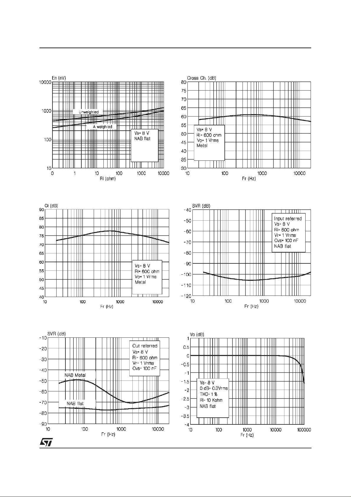
Figure 1: QuiescentCurrent vs. Supply Figure2: D.C. Outputvs. SupplyVoltage
Figure 3:
Figure 5:
Forward/ReverseThreshold
MuteThreshold
Figure4:
Figure6:
Metal/NormalThreshold
MuteAttenuationvs. Frequency
5/11

TDA7334
Figure 7: Mute Attenuationvs. Output Level Figure 8: THDvs. Frequency
Figure 9:
Figure 11:
THD + N vs. Frequency
LoadCharacteristic
Figure10:
Figure12:
THDvs. Supply Voltage
SignalHandling vs. Supply Voltage
6/11
TDA7334
Figure 13: Total Input Noisevs. Input Resistance Figure 14: Cross Channel vs. Frequency
Figure 15:
Figure 17:
CrossTalk vs. Frequency
SVRvs. Frequency
Figure16:
Figure18:
SVRvs. Frequency
PowerBandwidth
7/11

TDA7334
Figure 19:
VoltageGain vs. Input Voltage
Figure20:
NABNetwork
8/11

TDA7334
DIM.
MIN. TYP. MAX. MIN. TYP. MAX.
a1 0.51 0.020
B 0.77 1.65 0.030 0.065
b 0.5 0.020
b1 0.25 0.010
D 20 0.787
E 8.5 0.335
e 2.54 0.100
e3 17.78 0.700
F 7.1 0.280
I 5.1 0.201
L 3.3 0.130
Z 1.27 0.050
mm inch
OUTLINE AND
MECHANICAL DATA
DIP16
9/11

TDA7334
DIM.
MIN. TYP. MAX. MIN. TYP. MAX.
A 1.75 0.069
a1 0.1 0.25 0.004 0.009
a2 1.6 0.063
b 0.35 0.46 0.014 0.018
b1 0.19 0.25 0.007 0.010
C 0.5 0.020
c1 45°(typ.)
D (1) 9.8 10 0.386 0.394
E 5.8 6.2 0.228 0.244
e 1.27 0.050
e3 8.89 0.350
F (1) 3.8 4 0.150 0.157
G 4.6 5.3 0.181 0.209
L 0.4 1.27 0.016 0.050
M 0.62 0.024
S
mm inch
8°(max.)
OUTLINE AND
MECHANICAL DATA
SO16 Narrow
(1) D andF do not includemold flash or protrusions. Mold flash or potrusions shall not exceed 0.15mm(.006inch).
10/11

TDA7334
Information furnished is believed to be accurate and reliable. However, STMicroelectronics assumes no responsibility for the consequences
of use of such information nor for any infringement of patents or other rights of third parties which may result from its use. No license is
granted by implication or otherwise under any patent or patent rights of STMicroelectronics. Specification mentioned in this publication are
subject to change without notice. This publication supersedes and replaces all information previously supplied. STMicroelectronics products
are not authorized for use as critical components in life support devices or systems without express written approval of STMicroelectronics.
Australia - Brazil - China - Finland - France - Germany- Hong Kong - India - Italy - Japan - Malaysia - Malta - Morocco -
The ST logo is a registered trademark of STMicroelectronics
1999 STMicroelectronics – Printed in Italy – AllRights Reserved
Singapore - Spain - Sweden - Switzerland - United Kingdom - U.S.A.
STMicroelectronics GROUP OF COMPANIES
http://www.st.com
11/11
 Loading...