

SINGLE CHIP RDS DEMODULATOR + FILTER
VERYHIGH RDS DEMODULATION QUALITY
WITH IMPROVED DIGITAL SIGNAL PROCESSING
HIGH PERFORMANCE, 57KHz BANDPASS
FILTER (8th ORDER)
PURELY DIGITAL RDS DEMODULATION
WITHOUTEXTERNAL COMPONENTS
ARI INDICATION AND RDS SIGNAL QUALITY OUTPUTS
4.332MHzCRYSTALOSCILLATOR
(8.664 and 17.328MHz SELECTABLE OPTIONS)
LOW NOISE CMOS TECHNOLOGY
LOW RADIATION
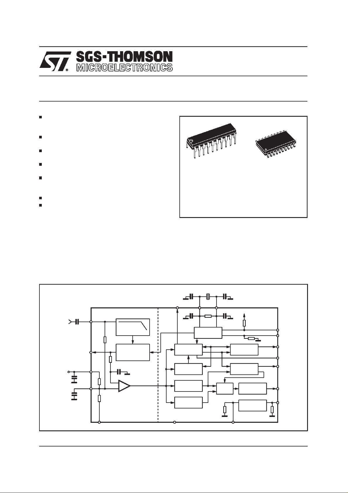
TDA7331
DIP20 SO20
ORDERING NUMBERS:
TDA7331 TDA7331D
DESCRIPTION
The TDA7331, an improved version of
TDA7330B, recovers the additional inaudible
RDS informationwhich is transmittedby FM radio
broadcasting stations and operates in accordance with the EBU (European Broadcasting Union) specifications.
The device is made up of two sections: a cas-
BLOCK DIAGRAM and TESTCIRCUIT
FILOUT
1
2nd ORDER
ANTIALIASING
FILTER
4
16
2VREF
8th ORDER
SC-BANDPASS
FILTER
-
+
MPX
V
S
100nF
10µF
270pF
caded antialiasing + switched capacitors bandpass filter for precise RDS band selection and a
demodulatingsection that performs the extraction
od RDS data stream (RDDA) and clock (RDCL),
to be furher processed by a suitable RDS decoder.
Outputs for RDS signal quality and ARI indication
are also present.
4.332MHz C2 47pFC1 27pF
T57
11
57KHz PLL
FAST
INDICATOR
POLARITY
BIPHASEDEC.
INTEGRAL
BIPHASEDEC.
OSCILLATOR
ARI
DIVIDER
OSCOUTOSCIN
910
3
&
1187.5Hz
PLL
QUAL DET.
0
MUX
1
DIFF. DECODER
TEST LOGIC
OSEL
18
FSEL
12
RDCL
15
ARI
14
QUAL
13
RDDA
19
TM
February 1998
5
GND N.C.
6,7,8,17
EXTRES
20
D97AU686B
1/7
TDA7331
ABSOLUTE MAXIMUM RATINGS
Symbol Parameter Value Unit
V
T
op
T
stg
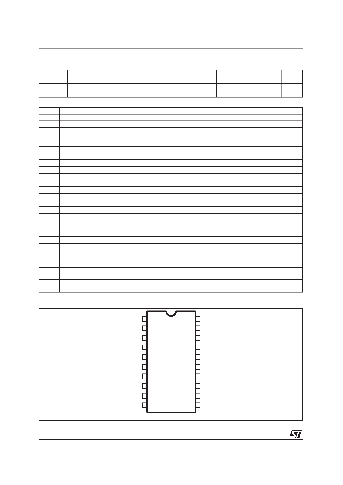
PIN FUNCTION
Nopin Name Functional description
1 MPX RDS inputsignal
2 VREF Reference voltage
3 OSEL Oscillator selector pin: - open, or closed to Vs = quartz oscillator
4 FILOUT Filter output
5 GND Ground
6 nc Not connected
7 nc Not connected
8 nc Not connected
9 OSCOUT Oscillator output
10 OSCIN Oscillator input
11 T57 Testing output pin: 57kHz clock output
12 RDCL RDS clock output 1187.5Hz
13 RDDA RDS dataoutput
14 QUAL Output for signal quality indication (High = good)
15 ARI Output for ARI indication: - high whenRDS+ARI arepresent
16 Vs Supply voltage
17 nc Not connected
18 FSEL Frequency selector pin: - 100K to V
19 TM Test mode pin: - open = normal operation
20 EXTRES Reset pin: - open = run mode
Supply Voltage 7 V
S
Operating Temperature Range -40 to 85
Storage Temperature -55 to 150
- closed to GND = external driven
- high when only ARI is present
- low when only RDS is present
- undefined when nos signal is present
= 17.328MHz
S
S
= testmode
S
= 8.664MHz
- closed to V
-closed to V
- open = 4.332MHz
- closed to V
= reset condition
S
C
°
C
°
PIN CONNECTION
2/7
MPX
VREF
OSEL
FILOUT
GND
N.C.
N.C.
N.C.
OSCOUT
1
2
3
4
5
6
7
8
9 RDCL
OSCIN 10 T5711
D97AU687
19
18
17
16
15
14
13
12
EXTRES20
TM
FSEL
N.C.
V
S
ARI
QUAL
RDDA
TDA7331
THERMAL DATA
Symbol Description DIP20 SO20 Unit
R
th j-amb
Thermal Resistance Junction-Ambient Max 100 200
C/W
°
ELECTRICALCHARACTERISTICS (T
=25°C, VS=5V, unlessotherwisespecified).
amb
Symbol Parameter Test Condition Min. Typ. Max. Unit
V
S
I
S
Supply voltage 4.5 5 5.5 V
Supply current 7.5 11.0 mA
FILTER
f
C
BW 3dBBandwidth 2.5 3 3.5 kHz
G Gain f = 57kHz 18 20 22 dB
A Attenuation
R
R
L
S/N Signal to noise ratio V
V
IN
V
REF
Center frequency 56.5 57 57.5 kHz
4kHz 18 22 dB
∆f±
f = 38kHz 50 60 dB
f = 67kHz 35 45 dB
Input impedance of MPX 80 120 150 K
I
Load impedance on FILOUT 1 M
=3mV
IN
RMS
30 40 dB
MPX input signal f = 19kHz; T3 ≤ 40dB(1)
f = 57kHz (RDS+ ARI)
Reference VS/2 V
100050mV
mV
DEMODULATOR
Input pins (EXTRES, FSEL, TM) all with internal pull down resistor
Input pin (OSEL) with internal pull up resistor
I
PD
I
PU
V
IH
V
IL
Input Current VIN= 5V (pull-down input) 15 30
Input Current VIN= 0V (pull-up input) -25 -10
Input voltage high 0.7⋅VS0.8⋅V
S
Input voltage low 0.2 ⋅ VS0.3⋅ V
S
Output pins (RDCL, RDDA, ARI, QUAL, T57)
V
OH
V
OL
Ouput voltage high IL= 0.5mA 4 4.6 V
Output voltage low IL= 0.5mA 0.4 1 V
OSCILLATOR
VCLL Input level OSCIN pin OSEL= open circuit 1 V
VCLH Input level OSCIN pin OSEL= open circuit 4 V
Amplitude OSCOUT OSEL= open circuit 4.5 V
V
PP
Amplitude OSCIN
(for external drive)
(1) The 3rd harmonic (57kHz) must be less than -40dB with respect to the input signal plus gain.
OSEL = GND,
f = 4.332MHz
OSEL = GND,
f = 8.664MHz
OSEL = GND,
f = 17.328MHz
100 mVpp
120 mVpp
150 mVpp
µ
µ
Ω
Ω
RMS
RMS
A
A
V
V
3/7
TDA7331
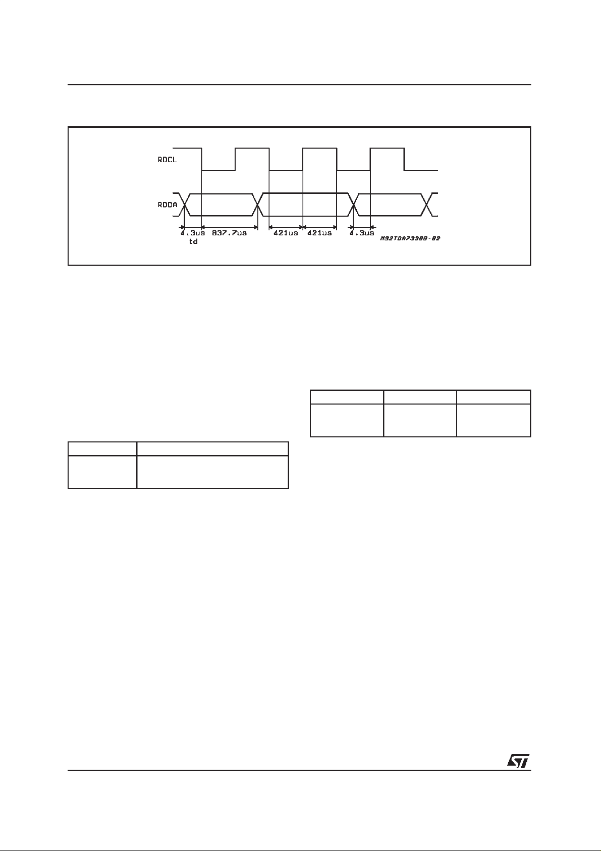
Figure 1. RDS timing diagram
CLOCK
LINE
DATA
LINE
OUTPUT TIMING
The RDS (1187.5Hz) output clock on RDCL line
is synchronizedto the incoming data.
According to the internal PLL lock condition data
change can result on the falling or on the rising
clock edge. (see Fig. 1)
Whichever clock edge is used by the decoder
(rising or falling edge) the data will remain valid
for 416.7 µsec after the clock transition.
OSCILLATORCONTROLS (FSEL, OSEL)
Three different crystal frequencies can be used.
The adaption of the internal clock divider to the
external crystal is achieved via the input pin
FSEL. See the followings table for reference:
Crystal FSEL (pin configuration)
4.332MHz
8.664MHz
17.328MHz
connected to GND or open
connected toVs
external resistor of 100K to Vs
A special mode is introduced to reduce EMI. With
pin OSEL connected to GND the internal oscillator is switched off and an external sinusoidal frequency could be applied on OSCIN. The peak to
peak voltage of this signal can be reduced down
to 60mV.
In this mode the frequency selection via FSEL is
still active.
Suggestedvalues of C1 and C2 are shown in the
followingtable:
Crystal C1 C2
4.332MHz
8.664MHz
17.328MHz
27pF
27pF
27pF
47pF
-
-
4/7
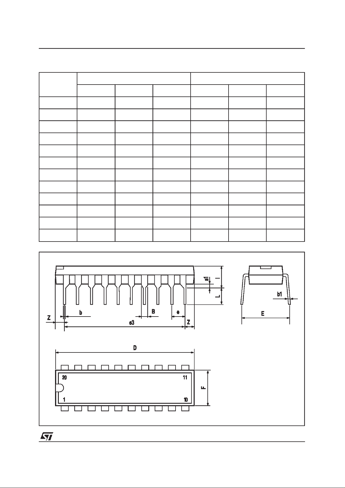
DIP20 PACKAGE MECHANICAL DATA
TDA7331
DIM.
MIN. TYP. MAX. MIN. TYP. MAX.
a1 0.254 0.010
B 1.39 1.65 0.055 0.065
b 0.45 0.018
b1 0.25 0.010
D 25.4 1.000
E 8.5 0.335
e 2.54 0.100
e3 22.86 0.900
F 7.1 0.280
I 3.93 0.155
L 3.3 0.130
Z 1.34 0.053
mm inch
5/7
TDA7331
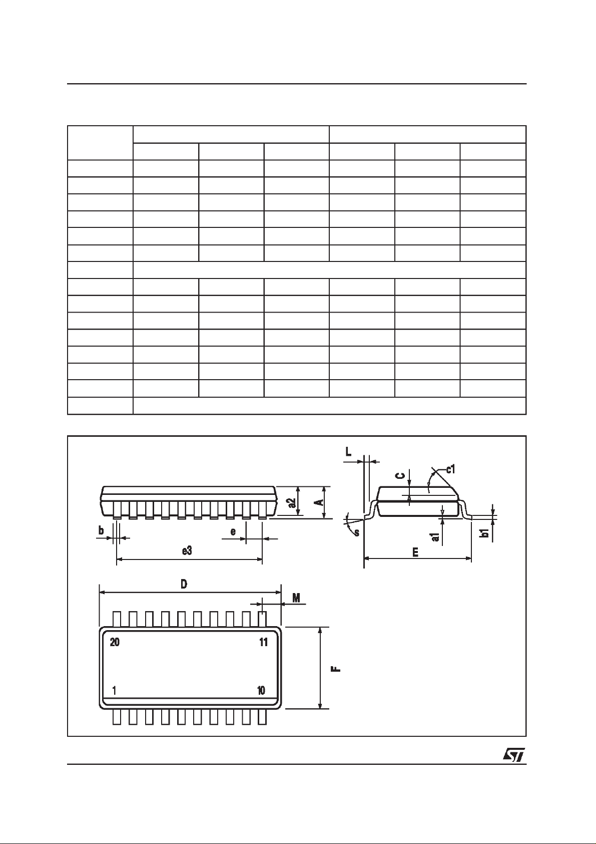
SO20 PACKAGEMECHANICAL DATA
DIM.
MIN. TYP. MAX. MIN. TYP. MAX.
A 2.65 0.104
a1 0.1 0.3 0.004 0.012
a2 2.45 0.096
b 0.35 0.49 0.014 0.019
b1 0.23 0.32 0.009 0.013
C 0.5 0.020
c1 45 (typ.)
D 12.6 13.0 0.496 0.512
E 10 10.65 0.394 0.419
e 1.27 0.050
e3 11.43 0.450
F 7.4 7.6 0.291 0.299
L 0.5 1.27 0.020 0.050
M 0.75 0.030
S 8 (max.)
mm inch
6/7

TDA7331
Information furnished is believed to be accurate and reliable.However, SGS-THOMSON Microelectronicsassumes no responsibility for the
consequences of use of such information nor for any infringementof patentsor other rights of third parties which may result fromits use. No
license is granted by implication or otherwise under any patent or patent rights of SGS-THOMSON Microelectronics. Specification mentioned in this publication are subject to change without notice.This publication supersedes and replaces all information previously supplied.
SGS-THOMSON Microelectronics products are not authorized for use as critical components in life support devices or systems without express written approval of SGS-THOMSON Microelectronics.
1998 SGS-THOMSON Microelectronics – Printed in Italy – All RightsReserved
SGS-THOMSON Microelectronics GROUP OF COMPANIES
Australia - Brazil - Canada - China - France - Germany - Italy - Japan - Korea - Malaysia - Malta - Morocco - The Netherlands -
Singapore - Spain - Sweden - Switzerland- Taiwan - Thailand - United Kingdom - U.S.A.
7/7
 Loading...