

SINGLE CHIP RDS DEMODULATOR+ FILTER
HIGH PERFORMANCE, 57KHz BANDPASS
FILTER (8th ORDER)
FILTER ADJUSTMENTFREE AND WITHOUT
EXTERNALCOMPONENTS
PURELY DIGITAL RDS DEMODULATION
WITHOUTEXTERNALCOMPONENTS
ARI (SK INDICATION) AND RDS SIGNAL
QUALITYOUTPUT
4.332MHzCRYSTAL OSCILLATOR
(8.664MHzOPTIONAL)
LOW NOISE MIXED BIPOLAR/CMOS TECHNOLOGY
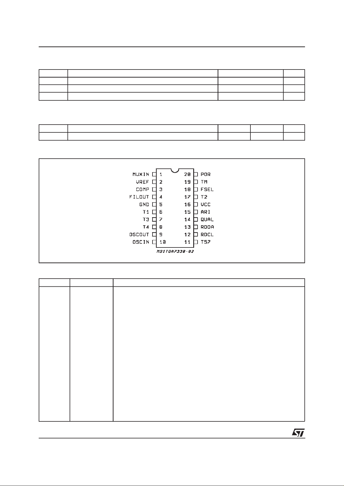
DESCRIPTION
The TDA7330B is a RDS demodulator. It recovers the additional inaudible RDS information
which is transmitted by FM radio broadcasting
stations.
The output data signal (RDDA) and clock signal
(RDCL) can be further processed by a suitable
RDS decoder (microprocessor).
The device operates in accordancewith the EBU
(European BroadcastingUnion) specifications.
The IC includes a 2nd order antialiasing input fil-
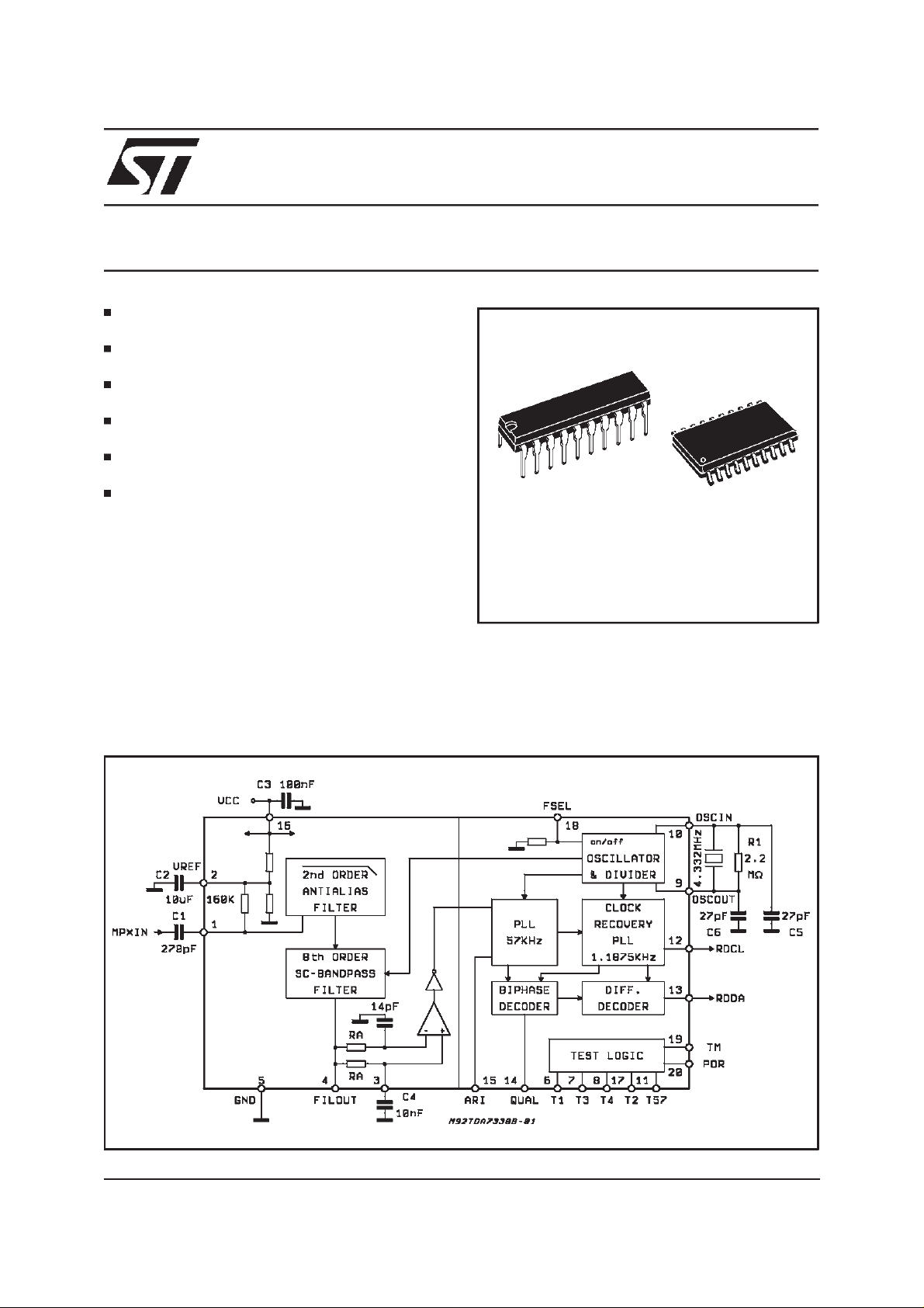
TDA7330B
DIP20 SO20
ORDERING NUMBERS:
TDA7330B TDA7330BD
ter, a 57KHz switched capacitor band pass filter,
a smoothing filter and cross detector, a bit rate
clock recovery circuit, a 57KHz PLL, BI-PHASE
PSK decoder, differential decoding circuit, ARI indication and RDS signalquality output.
BLOCK DIAGRAM
November 1999
1/9
TDA7330B
ABSOLUTE MAXIMUM RATINGS
Symbol Parameter Value Unit
V
CC
T
op
T
stg
THERMAL DATA
Symbol Description DIP20 SO20 Unit
R
th j-case
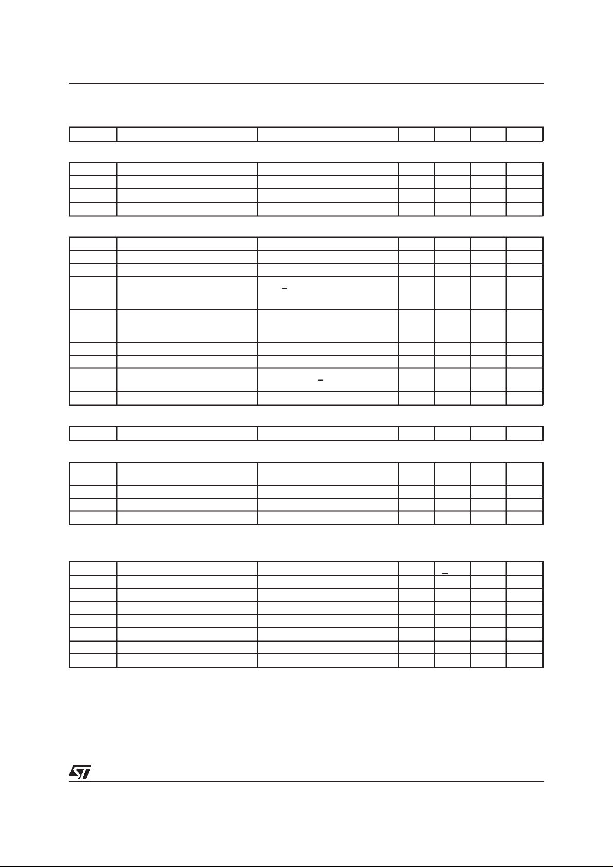
PIN CONNECTION(Topview)
Supply Voltage 7 V
Operating Temperature Range -40 to 85
Storage Temperature -40 to 150 °C
Thermal Resistance Junction-case Typ. 100 200 °C/W
C
°
PIN FUNCTION
Nr. Name Description
2/9
10
11
12
13
14
15
16
17
18
19
20
1
2
3
4
5
6
7
8
9
MUXIN
V
ref
COMP
FIL OUT
GND
T1
T3
T4
OSC OUT
OSC IN
T57
RDCL
RDDA
QUAL
ARI
V
CC
T2
FSEL
TM
POR
RDS input signal.
Reference voltage
Not inverting comparator input (smoothing filter)
Filter Output
Ground
Testing output pin (not to be used)
Testing output pin (not to be used)
Testing output pin (not to be used)
Oscillator output
Oscillator Input
Testing output pin: 57KHz clock output
RDS clock output (1187.5Hz)
RDS data output
Output for signal quality indication (High = good)
Output for ARI indication (High when RDS + ARIsignals are present)
(High when onlyARI is present)
(Low when only RDS is present)
(indefined when no signal is present)
Supply Voltage
Testing output pin (not to be used)
Frequency selector pin: open = 4.332MHz, closed to V
Test mode pin (open = normal RUN)
(closedto V
= Test mode)
CC
Reset Input for testing (active high)
= 8.664MHz
CC
TDA7330B
ELECTRICALCHARACTERISTICS (VCC= 5V, Tamb = 25°C; Rg = 600Ω; fosc = 4.332MHz;
V
= 20mVrmsunless otherwisespecified)
IN
Symbol Parameter Test Condition Min. Typ. Max. Unit
SUPPLY
V
I
R
POR
POR
CC
S
Supply Voltage 4.5 5 5.5 V
Supply Current 9 mA
POR Pull Down Resistor pin 20 40 KΩ
POR Threshold 2.5 V
ON
FILTER(measuredan pin 4 FILOUT)
F
BW 3dB Bandwidth 2.5 3 3.5 KHz
G Gain f = 57KHz 18 20 22 dB
A Attenuation ∆f = +4KHz
Ph Phase nonlinearity A (see note1)
∆
R
S/N Signal to Noise Ratio V
V
R
Center Frequency 56.5 57 57.5 KHz
C
f = 38KHz; V
f = 67KHz; V
= 500mVrms
i
= 250mVrms
i
18
50
35
22
80
50
0.5
B (see note1)
C (see note1)
Input Impedance 100 160 200 KΩ
i
= 3mVrms 30 40 dB
i
Maximum Input Signal Capability f= 19KHz;T3 < –40dB(seenote2)
i
1
2
f = 57KHz (RDS + ARI)
Load Impedance Pin 4 100 KΩ
L
5
7.5
10
1
50
CROSSDETECTOR
RA Resistance pin 3-4 15 21 28 KΩ
OSCILLATOR
dB
dB
dB
DEG
DEG
DEG
Vrms
mVrms
F
OSC
Oscillator Frequency F
= Open (*)
SEL
F
= Closed to VCC(**)
SEL
4.332
8.664
VCLL Clock Input level LOW (pin10) 1 V
VCLH Clock Input Level HIGH (pin 10) 4 V
Output Amplitude (pin 9) 4.5 V
(*) FSEL pin has an internal 40KΩ pull down resistor A 4.332MHz QUARTZ must be used (**)A 8.664MHz QUARTZ must be used.
DEMODULATOR
f
∆
S
RDS
S
ARI
T
lock
V
OH
V
OL
f
RDS
t
D
Note(1):
The phase non linearity isdefined as: ∆Ph = | -2φf2 + φf1 + φf3 |
where φfx is the input-output phase difference at the frequency fx (x = 1,2,3)
Max Oscillator Deviation F
O
= Open + 1.2 KHz
SEL
RDS Detection Sensitivity 1 mVrms
ARI Detection Sensitivity 3 mVrms
RDS Lockup Time 100 ms
Output HIGH Voltage IL= 0.5mA; pins 12,13, 14, 15 4 V
Output LOW Voltage IL= 0.5mA; pins 12, 13, 14, 15 1 V
Data Rate for RDS RDCL pin 1187.5 Hz
RDDA Transition versus RDCL (see figure 2) 4.3 µsec
MHz
MHz
PP
3/9

TDA7330B
ELECTRICALCHARACTERISTICS
Measure f1 (KHz) f2 (KHz) f3 (KHz) ∆Ph max
A 56.5 57 57.5 <5
B 56 57 58 <7.5°
C 55.5 57 58.5 <10°
Note(2):
Figure 2:
The 3th harmonic (57KHz) must be less than-40dB in respect to the input signal 19KHz plus gain.
RDS timing diagram
(continued)
°
OUTPUT TIMING
The generated 1187.5Hz output clock (RDCL
line) is synchronizedto the incoming data.
According to the internal PLL lock condition this
Figure 3:
Test Circuit
data change can results on the falling or on the
rising clock edge.
Whicheverclock edge is usedbythe decoder(rising or falling edge) the data will remain valid for
416.7µsecafter the clocktransition.
4/9

TDA7330B
APPLICATIONSUGGESTION
A good DC decoupling between V
CC
GROUND is necessary: a 100nF ceramic capacitor, with lowresistance and low inductance
at high frequency,directly connectedon pin 16
(V
)and 5 (GND) is recommended.
CC
A small series inductance (100µH) or resistor
(27Ω) may be used for supply linefiltering.
and
The Layout path pin2 - C2 - pin5 must be as
shortas possible.
If the supply line, after the power on has a soft
and disturbed (spikes) slope, a capacitor of
100nF, between POR and V
mended.
The varioustesting pins have no sense for the
customer.
Figure 4: P.C. board and componentlayout of fig. 3 (1:1 scale)
, is racom-
CC
5/9

TDA7330B
Figure 5: Gain vs. Frequency Figure6: GroupDelay vs. Frequency
6/9

TDA7330B
DIM.
MIN. TYP. MAX. MIN. TYP. MAX.
a1 0.254 0.010
B 1.39 1.65 0.055 0.065
b 0.45 0.018
b1 0.25 0.010
D 25.4 1.000
E 8.5 0.335
e 2.54 0.100
e3 22.86 0.900
F 7.1 0.280
I 3.93 0.155
L 3.3 0.130
Z 1.34 0.053
mm inch
OUTLINE AND
MECHANICAL DATA
DIP20
7/9
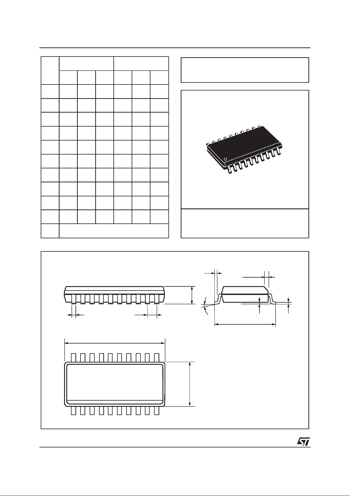
TDA7330B
DIM.
MIN. TYP. MAX. MIN. TYP. MAX.
A 2.35 2.65 0.093 0.104
A1 0.1 0.3 0.004 0.012
B 0.33 0.51 0.013 0.020
C 0.23 0.32 0.009
D 12.6 13 0.496 0.512
E 7.4 7.6 0.291 0.299
e 1.27 0.050
H 10 10.65 0.394 0.419
h 0.25 0.75 0.010 0.030
L 0.4 1.27 0.016 0.050
K0°(min.)8°(max.)
mm inch
0.013
OUTLINE AND
MECHANICAL DATA
SO20
B
e
D
1120
110
L
hx45°
A
K
A1
C
H
E
SO20MEC
8/9

TDA7330B
Information furnished is believed to be accurate and reliable. However, STMicroelectronics assumes no responsibility for the consequences
of use of such information nor for any infringement of patents or other rights of third parties which may result from its use. No license is
granted by implication or otherwise under any patent or patent rights of STMicroelectronics. Specificationmentioned in this publication are
subject to change without notice. This publicationsupersedes and replaces all information previously supplied. STMicroelectronics products
are not authorized for use as critical components in life support devices or systems without express written approval of STMicroelectronics.
The ST logo is a registered trademark of STMicroelectronics
1999 STMicroelectronics – Printed in Italy – All Rights Reserved
STMicroelectronics GROUPOF COMPANIES
Australia - Brazil - China - Finland- France - Germany - HongKong - India - Italy - Japan - Malaysia - Malta - Morocco -
Singapore - Spain -Sweden - Switzerland - United Kingdom - U.S.A.
http://www.st.com
9/9
 Loading...