

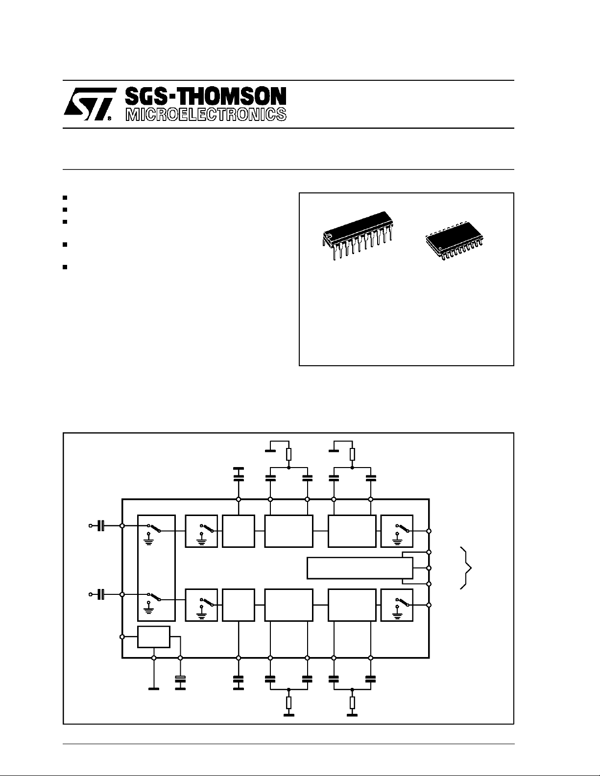
3 BAND DIGITALCONTROLLED AUDIO PROCESSOR
ONE STEREOINPUT
ONE STEREOOUTPUT
TWO INDEPENDENT VOLUME CONTROL IN
1.0dBSTEPS
TREBLE, MIDDLE AND BASS CONTROL IN
1.0dBSTEPS
ALL FUNCTIONS PROGRAMMABLE VIA SE-
2
RIAL I
DESCRIPTION
The TDA7319 is a volume and tone (bass , middle and treble) processor for quality audio applicationin car radio and Hi-Fi system.
Control is accomplished by serial I
processorinterface.
The AC signal setting is obtained by resistor networks and switches combined with operational
amplifiers.
CBUS
2
C bus micro-
TDA7319
DIP20 SO20
ORDERING NUMBERS: TDA7319 (DIP20)
TDA7319D (SO20)
Thanks to the used BIPOLAR/MOS Technology,
Low Distortion, Low Noise and Low Dc stepping
areobtained.
BLOCK DIAGRAM ANDAPPLICATION CIRCUIT
C3
5.6nF
C1 2.2µF
C2 2.2µF
2
L
19
R
1
V
S
SUPPLY
12 20 18 17 16 15 14
1st VOL
TREBLE
1st VOL
TREBLE
CREFAGND
TREBLE(R) MOUT(R)MIN(R) BOUT(R)BIN(L)
REF
C4
5.6nF
C
10µF
R1
2.7K
C5
15nF
MOUT(L)TREBLE(L) MIN(L) BOUT(L)BIN(L)
MIDDLE BASS
MIDDLE BASS
C7
15nF
C6
22nF
SERIAL BUS DECODE &LATCHES
22nF
R2
2.7K
C8
100nF
C11
100nF
C9
5.6K
R4
5.6K
R3
76543
C10
100nF
2nd VOL
2nd VOL
C12
100nF
10
11
13
8
9
OUT L
SCL
SDA
DIGGND
OUT R
D93AU042E
2
I
BUS
C
May 1995
1/16
TDA7319
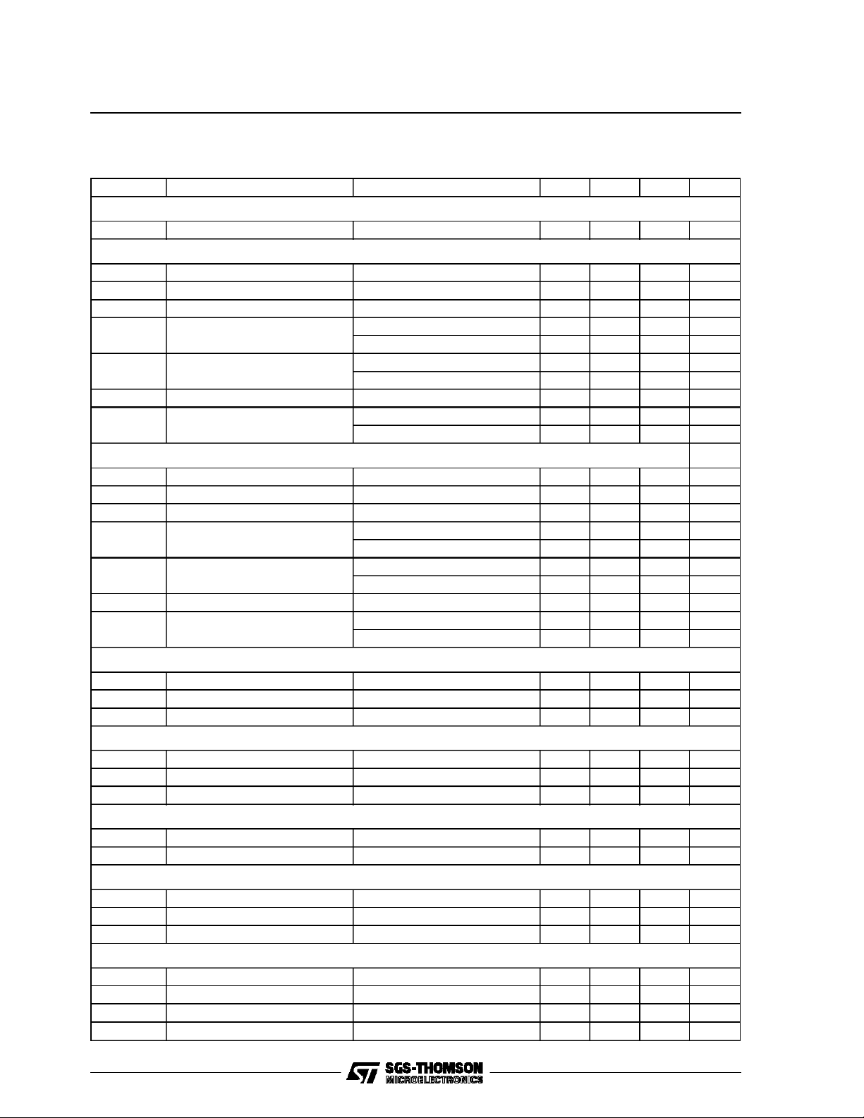
ABSOLUTE MAXIMUMRATINGS
Symbol Parameter Value Unit
V
S
T
amb
T
stg
PIN CONNECTION
Operating Supply Voltage 10.5 V
Operating Ambient Temperature -40 to 85 °C
Storage Temperature Range -55 to 150 °C
V
IN L
TREBLE L
MINL
M OUT L
BINL
B OUT L
OUT L
SDA
S
1
2
3
4
5
6
7
8
9 GND
20
19
18
17
16
15
14
13
12
C
REF
IN R
TREBLE R
MINR
M OUT R
BINR
B OUT R
OUT R
SCL 10 DIG GND11
D93AU041A
THERMAL DATA
Symbol Parameter DIP20 SO20 Unit
R
th j-amb
Thermal Resistance Junction-pins 150 150 °C/W
QUICK REFERENCEDATA
Symbol Parameter Min. Typ. Max. Unit
V
S
V
CL
THD Total Harmonic Distortion V = 1Vrms f = 1KHz 0.01 0.08 %
S/N Signal to Noise Ratio 106 dB
S
C
2/16
Supply Voltage 6 9 10.5 V
Max. inputsignal handling 2 Vrms
Channel Separation f = 1KHz 100 dB
1st and 2nd Volume Control 1dB step -47 0 dB
Bass, Middle and TrebleControl 1dB step -14 +14 dB
Mute Attenuation 100 dB
TDA7319
ELECTRICAL CHARACTERISTICS (VS= 9V; RL= 10KΩ; f = 1KHz; all control = flat (G = 0); T
25°C Refer to thetest circuit,unless otherwisespecified.)
Symbol Parameter Test Condition Min. Typ. Max. Unit
INPUT
R
in
Input Resistance 35 50 65 KΩ
1st VOLUME CONTROL
C
RANGE
A
VMAX
A
A
V
step
E
E
mute
A
t
DC
Control Range 45 47 49 dB
Maximum Attenuation 45 47 49 dB
Step Resolution 0.5 1.0 1.5 dB
Attenuation Set Error G = 0to -24dB -1.0 1.0 dB
G = -24 to -47dB -1.5 1.5 dB
Tracking Error G = 0 to -24dB 1 dB
G = 24 to -47dB 2 dB
Mute Attenuation 80 100 dB
DC Steps Adiacent Attenuation Steps 0 3 mV
From 0dB to A
VMAX
0.5 5 mV
2nd VOLUME CONTROL
C
RANGE
A
VMAX
A
A
V
step
E
A
E
t
MUTE
DC
Control Range 45 47 49 dB
Maximum Attenuation 45 47 49 dB
Step Resolution 0.5 1.0 1.5 dB
Attenuation Set Error G = 0to -24dB -1.0 1.0 dB
G = -24 to -47dB -1.5 1.5 dB
Tracking Error G = 0 to -24dB 1 dB
G = 24 to -47dB 2 dB
Mute Attenuation 80 100 dB
DC Steps Adiacent Attenuation Steps 0 3 mV
From 0dB to A
VMAX
0.5 5 mV
BASS
C
RANGE
A
R
b
step
Internal Feedback Resistance 32 44 56 KΩ
Control Range ±11.5 ±14 ±16 dB
Step Resolution 0.5 1 1.5 dB
MIDDLE
C
RANGE
A
R
b
step
Internal Feedback Resistance 18 25 32 KΩ
Control Range ±11.5 ±14 ±16 dB
Step Resolution 0.5 1 1.5 dB
TREBLE
C
RANGE
A
step
Control Range ±13 ±14 ±15 dB
Step Resolution 0.5 1 1.5 dB
SUPPLY
V
S
I
S
SVR Ripple Rejection 60 90 dB
Supply Voltage (note1) 6 9 10.5 V
Supply Current 4 7 10 mA
amb
=
AUDIO OUTPUT
V
clip
R
Ol
R
O
V
DC
Clipping Level d = 0.3% 2 2.6 Vrms
Output Load Resistance 2 KΩ
Output Impedance 100 180 300 Ω
DC Voltage Level 3.8 V
3/16
TDA7319
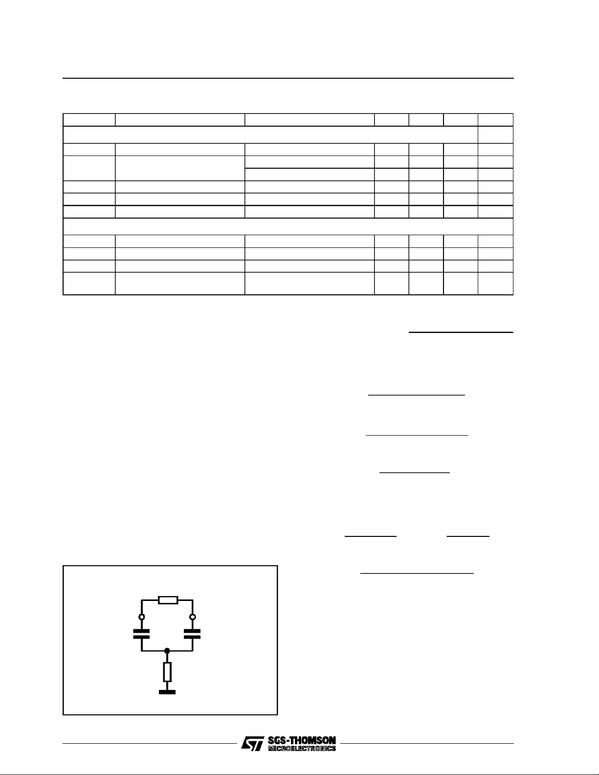
ELECTRICAL CHARACTERISTICS (continued)
Symbol Parameter Test Condition Min. Typ. Max. Unit
GENERAL
e
NO
E
t
S/N Signal to Noise Ratio All Gains = 0dB; V
S
C
d Distortion A
BUS INPUTS
V
il
V
ih
I
in
V
O
Note 1: the device is functionally good at Vs = 5V. A step down, on VS, to 4V does’t reset the device.
Output Noise All Gains0dB(B= 20to 20kHzflat) 5 15 µV
Total Tracking Error AV = 0 to -24dB 0 1 dB
= -24 to -47dB 0 2 dB
A
V
=1V
O
rms
Channel Separation 80 100 dB
=0;Vin=1V
V
Input Low Voltage 1V
Input High Voltage 3 V
Input Current Vin = 0.4V -5 5 µA
Output Voltage SDA
Acknowledge
IO= 1.6mA 0.4 0.8 V
rms
106 dB
0.01 0.08 %
APPLICATION SUGGESTIONS
The first and the last stages are volume control
blocks. The control range is 0 to -47dB (mute)
with a 1dB step.
Thevery high resolution allowsthe implementation
ofsystems freefromany noisyacousticaleffect.
The TDA7319 audioprocessor provides 3 bands
tones control.
Bass, Middle Stages
The Bass and the middle cells have the same
structure.
The Bass cell has an internal resistor Ri = 44KΩ
typical.
The Middle cell has an internalresistor Ri = 25KΩ
typical.
Severalfilter types can be implemented,connecting external components to the Bass/Middle IN
and OUTpins.
Figure1.
Ri internal
OUTIN
4/16
C
1
R
2
D95AU313
C
2
The fig.1 refers to basic T Type Bandpass Filter
starting from the filter component values (R1 internal and R2,C1,C2 external) the centre frequency Fc, the gain Av at max. boost and the filter Q factor are computedas follows:
=
F
C
1
2 ⋅ π ⋅√Ri,R2, C1, C2
R2 C2+ R2 C1 + Ri C1
A
=
V
R2 C1 + R2C2
√Ri R2 + C1 C2
Q =
R2 C1 + R2 C2
Viceversa,once Fc, Av, and Ri internal value are
fixed, the external components values will be:
2
Q
⋅ C1
− 1Q
2
A
V
2
C1 =
− 1
A
V
2 ⋅ π ⋅ R
R2 =
⋅ Q
i
− 1− Q
A
V
2 ⋅ π ⋅ C1 ⋅ FC⋅ (AV− 1) ⋅Q
C2 =
Treble Stage
The treble stage is a high pass filter whose time
constant is fixed by an internal resistor (25KΩ
typical) and an external capacitor connected betweentreble pins and ground
Typicalresponsesare reportedin Figg.10 to 13.
CREF
The suggested 10µF reference capacitor (CREF)
value can be reduced to 4.7µF if the application
requiresfaster powerON.
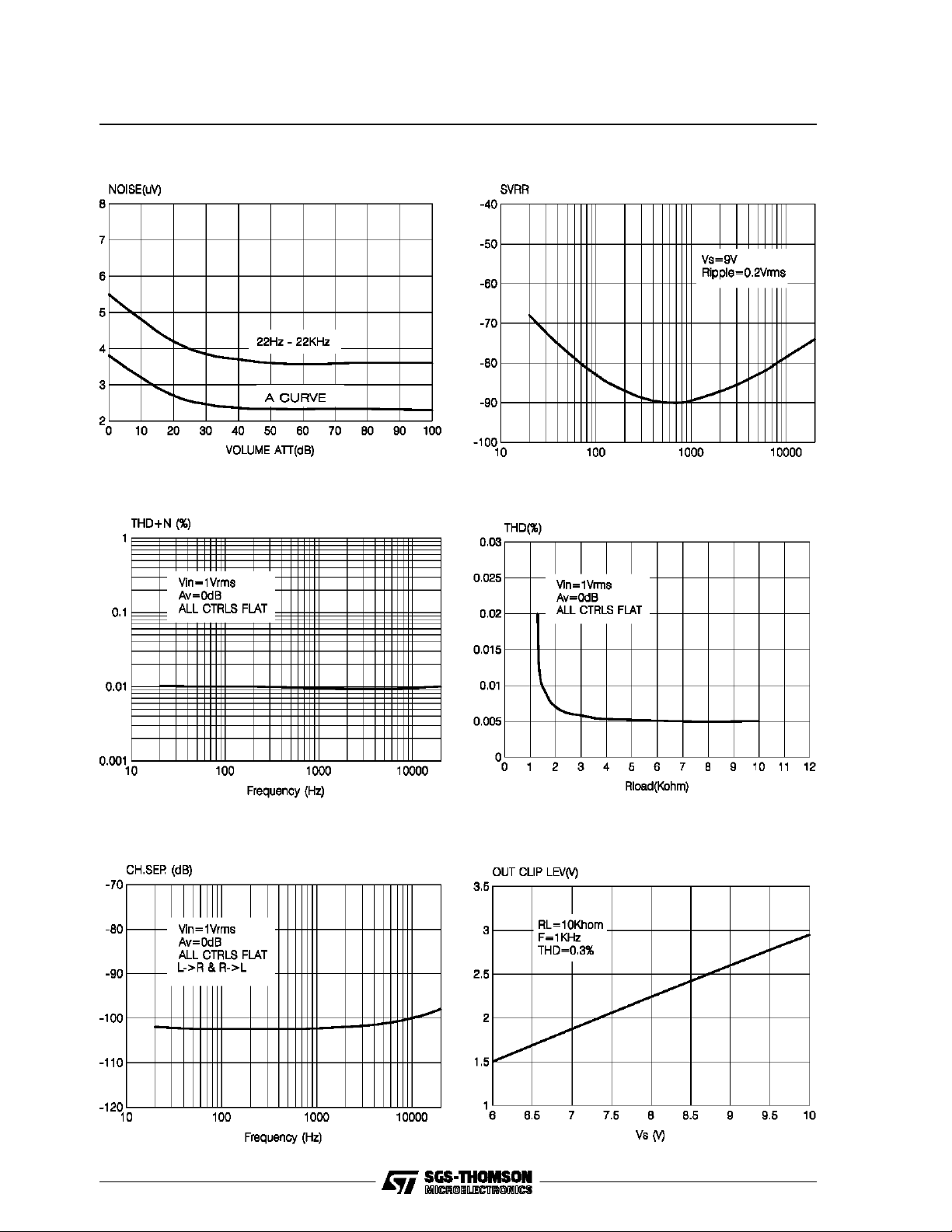
Figure2: Noisevs. volume setting Figure3: SVRRvs. frequency
TDA7319
Figure4: THDvs. frequency Figure5: THDvs. R
LOAD
Figure6: Channelseparation vs. frequency Figure7: Outputclip level vs. Supplyvoltage
5/16

TDA7319
Figure8: Quiescentcurrent vs.supply voltage Figure9: Quiescentcurrent vs. temperature
Figure10: Bass response Figure 11: Middleresponse
= 25kΩ
R
i
R
=44kΩ
i
C9 = C10 = 100nF (Bout, Bin)
R3 = 5.6kΩ
C9 = 15nF (MIN)
C6 - 22nF (MOUT)
R1 = 2.7kΩ
Figure12: Trebleresponse Figure 13: Typical tone response
C
6/16
TREBLE
= 5.6nF

2
C BUS INTERFACE
I
Data transmission from microprocessor to the
TDA7319 and viceversa takes place thru the 2
wires I
2
C BUS interface, consisting of the two
lines SDA and SCL (pull-up resistors to positive
supplyvoltage must beexternally connected).
DataValidity
As shown in fig. 3, the data on the SDA line must
be stable during the high period of the clock. The
HIGH and LOW state of the data line can only
change when the clock signal on the SCL line is
LOW.
Startand Stop Conditions
As shown in fig.4 a start condition is a HIGH to
LOW transition of the SDA line while SCL is
HIGH. The stop condition is a LOW to HIGH transitionof the SDAline while SCL is HIGH.
Byte Format
Every byte transferred to the SDA line must contain 8 bits. Each byte must be followed by an acknowledgebit. TheMSB is transferredfirst.
TDA7319
Acknowledge
The master (µP) puts a resistive HIGH levelon the
SDA line during the acknowledge clock pulse (see
fig. 5). The peripheral (audioprocessor) that acknowledges has to pull-down (LOW) the SDA line
during the acknowledge clock pulse, so that the
SDAlineis stableLOW duringthisclockpulse.
The audioprocessor which has been addressed
has to generate an acknowledge after the receptionof each byte, otherwise the SDA line remains
at the HIGH level during the ninth clock pulse
time. In this case the master transmitter cangenerate the STOP information in order to abort the
transfer.
Transmissionwithout Acknowledge
Avoiding to detect the acknowledgeof the audioprocessor, the µP can use a simplier transmission: simply it generates the 9th clock pulse without checking the slave acknowledging, and then
sends the newdata.
This approach of course is less protected from
misworking and decreasesthe noise immunity.
2
DataValidity on the I
CBUS
TimingDiagram of I2CBUS
2
Acknowledgeon the I
CBUS
7/16

TDA7319
SDA, SCL I2CBUSTIMING
Symbol Parameter Min. Typ. Max. Unit
f
SCL
t
BUF
t
HD:STA
t
LOW
t
HIGH
t
SU:STA
t
HD:DA
t
SU:DAT
t
R
t
F
t
SU:STO
All values referred to V
(*) Must be guaranteed by the I
SCL clock frequency 0 400 kHz
Bus free time betweena STOP and START condition 1.3 µs
Hold time (repeated) START condition. After this period, the first
0.6 µs
clock pulse is generated
LOW period of the SCL clock 1.3 µs
HIGH periodof the SCL clock 0.6 µs
Set-up time for a repeated START condition 0.6 µs
Data hold time 0.300 µs
Data set-up time 100 ns
Rise time of both SDA and SCL signals 20 300 ns (*)
Fall time of both SDA and SCL signals 20 300 ns (*)
Set-up time for STOP condition 0.6 µs
IH min.
and V
levels
IL max.
2
C BUS master.
Definition of timing on the I2C-bus
SDA
t
SCL
PS
P = STOP
S = START
BUF
t
HD;STA
t
LOW
t
RtF
t
HD;DAT
t
HIGH
t
t
HD;STA
t
t
SU;DAT
SU;STA
Sr P
D95AU314
t
F
SU;STO
t
SP
8/16

TDA7319
SOFTWARE SPECIFICATION
InterfaceProtocol
The interfaceprotocol comprises:
A start condition (s)
A chip address byte, containing the TDA7319
TDA7319 ADDRESS
MSB
S100001A0
ACK = Acknowledge
S = Start
P = Stop
MAX CLOCK SPEED 400kbits/s
first byte
LSB MSB LSB MSB LSB
ACK DATA ACK DATA AC K P
address(the 8th bit of the byte must be 0). The
TDA7319must always acknowledge at theend
ofeach transmittedbyte.
A sequenceof data (N-bytes + acknowledge)
A stop condition (P)
Data Transferred (N-bytes + Acknowledge)
SOFTWARE SPECIFICATION
Chip address
1
MSB
0000110
FUNCTION CODES
MSB F6 F5 F4 F3 F2 F1 LSB
1st VOLUME 0 F6F5F4F3F2F1 0
2nd VOLUME 0 F6F5F4F3F2F1 1
TREBLE 1 0 0 F4F3F2F1F0
MIDDLE 1 0 1 F4F3F2F1F0
BASS 1 1 0 F4F3F2F1F0
MUTMUX 1 1 1 F4F3F2F1F0
POWERON RESET:
1st volume = 2nd volume = Mute
Treble= Middle = Bass = -14dB
Mutmux= Active Input
LSB
9/16

TDA7319
1stVOLUME CODES
MSB F6 F5 F4 F3 F2 F1 LSB FUNCTION
0 0 step 1dB
0 0 0 0dB
0 0 1 -1dB
0 1 0 -2dB
0 1 1 -3dB
1 0 0 -4dB
1 0 1 -5dB
1 1 0 -6dB
1 1 1 -7dB
0 0 step 8dB
000 0dB
0 0 1 -8dB
0 1 0 -16dB
0 1 1 -24dB
1 0 0 -32dB
1 0 1 -40dB
1 1 1 MUTE
2nd VOLUME CODES
MSB F6 F5 F4 F3 F2 F1 LSB FUNCTION
0 1 step 1dB
0 0 0 0dB
0 0 1 -1dB
0 1 0 -2dB
0 1 1 -3dB
1 0 0 -4dB
1 0 1 -5dB
1 1 0 -6dB
1 1 1 -7dB
0 1 step 8dB
000 0dB
0 0 1 -8dB
0 1 0 -16dB
0 1 1 -24dB
1 0 0 -32dB
1 0 1 -40dB
1 1 1 MUTE
10/16

TREBLECODES
MSB F6 F5 F4 F3 F2 F1 LSB FUNCTION
1 0 0 TREBLE BOOST
00000 0dB
00001 1dB
00010 2dB
00011 3dB
00100 4dB
00101 5dB
00110 6dB
00111 7dB
01000 8dB
01001 9dB
0 1 0 1 0 10dB
0 1 0 1 1 11dB
0 1 1 0 0 12dB
0 1 1 0 1 13dB
0 1 1 1 0 14dB
0 1 1 1 1 14dB
1 0 0 TREBLE CUT
10000 0dB
1 0 0 0 1 -1dB
1 0 0 1 0 -2dB
1 0 0 1 1 -3dB
1 0 1 0 0 -4dB
1 0 1 0 1 -5dB
1 0 1 1 0 -6dB
1 0 1 1 1 -7dB
1 1 0 0 0 -8dB
1 1 0 0 1 -9dB
1 1 0 1 0 -10dB
1 1 0 1 1 -11dB
1 1 1 0 0 -12dB
1 1 1 0 1 -13dB
1 1 1 1 0 -14dB
1 1 1 1 1 -14dB
TDA7319
11/16

TDA7319
MIDDLECODES
MSB F6 F5 F4 F3 F2 F1 LSB FUNCTION
1 0 1 MIDDLE BOOST
00000 0dB
00001 1dB
00010 2dB
00011 3dB
00100 4dB
00101 5dB
00110 6dB
00111 7dB
01000 8dB
01001 9dB
0 1 0 1 0 10dB
0 1 0 1 1 11dB
0 1 1 0 0 12dB
0 1 1 0 1 13dB
0 1 1 1 0 14dB
0 1 1 1 1 14dB
1 0 1 MIDDLE CUT
10000 0dB
1 0 0 0 1 -1dB
1 0 0 1 0 -2dB
1 0 0 1 1 -3dB
1 0 1 0 0 -4dB
1 0 1 0 1 -5dB
1 0 1 1 0 -6dB
1 0 1 1 1 -7dB
1 1 0 0 0 -8dB
1 1 0 0 1 -9dB
1 1 0 1 0 -10dB
1 1 0 1 1 -11dB
1 1 1 0 0 -12dB
1 1 1 0 1 -13dB
1 1 1 1 0 -14dB
1 1 1 1 1 -14dB
12/16

BASSCODES
MSB F6 F5 F4 F3 F2 F1 LSB FUNCTION
1 1 0 BASS BOOST
00000 0dB
00001 1dB
00010 2dB
00011 3dB
00100 4dB
00101 5dB
00110 6dB
00111 7dB
01000 8dB
01001 9dB
0 1 0 1 0 10dB
0 1 0 1 1 11dB
0 1 1 0 0 12dB
0 1 1 0 1 13dB
0 1 1 1 0 14dB
0 1 1 1 1 14dB
1 1 0 BASS CUT
10000 0dB
1 0 0 0 1 -1dB
1 0 0 1 0 -2dB
1 0 0 1 1 -3dB
1 0 1 0 0 -4dB
1 0 1 0 1 -5dB
1 0 1 1 0 -6dB
1 0 1 1 1 -7dB
1 1 0 0 0 -8dB
1 1 0 0 1 -9dB
1 1 0 1 0 -10dB
1 1 0 1 1 -11dB
1 1 1 0 0 -12dB
1 1 1 0 1 -13dB
1 1 1 1 0 -14dB
1 1 1 1 1 -14dB
TDA7319
MUTMUXCODES
MSB F6 F5 F4 F3 F2 F1 LSB FUNCTION
1 1 1 INPUTS
XXX00 NOTALLOWED
XXX01 NOTALLOWED
XXX10 NOTALLOWED
X1111 IN
13/16

TDA7319
SO20PACKAGE MECHANICAL DATA
DIM.
MIN. TYP. MAX. MIN. TYP. MAX.
A 2.65 0.104
a1 0.1 0.3 0.004 0.012
a2 2.45 0.096
b 0.35 0.49 0.014 0.019
b1 0.23 0.32 0.009 0.013
C 0.5 0.020
c1 45 (typ.)
D 12.6 13.0 0.496 0.512
E 10 10.65 0.394 0.419
e 1.27 0.050
e3 11.43 0.450
F 7.4 7.6 0.291 0.299
L 0.5 1.27 0.020 0.050
M 0.75 0.030
mm inch
S 8 (max.)
14/16

DIP20 PACKAGEMECHANICAL DATA
TDA7319
DIM.
MIN. TYP. MAX. MIN. TYP. MAX.
a1 0.254 0.010
B 1.39 1.65 0.055 0.065
b 0.45 0.018
b1 0.25 0.010
D 25.4 1.000
E 8.5 0.335
e 2.54 0.100
e3 22.86 0.900
F 7.1 0.280
I 3.93 0.155
L 3.3 0.130
mm inch
Z 1.34 0.053
15/16

TDA7319
Information furnished is believed to be accurate and reliable. However, SGS-THOMSON Microelectronics assumes no responsability for the
consequences of use of such information nor for any infringement of patents or other rights of thirdparties which may results from its use. No
license is granted by implication or otherwise under any patent or patent rights of SGS-THOMSON Microelectronics. Specifications mentioned in this publication are subject to change without notice. This publication supersedes and replaces all information previously supplied.
SGS-THOMSON Microelectronics products are not authorized for use as critical components in life support devices or systems withoutexpress written approval of SGS-THOMSON Microelectronics.
1995 SGS-THOMSON Microelectronics - Printed in Italy - All Rights Reserved
Australia - Brazil - France - Germany - Hong Kong - Italy - Japan - Korea - Malaysia -Malta - Morocco - The Netherlands - Singapore -
SGS-THOMSON Microelectronics GROUP OF COMPANIES
Spain - Sweden - Switzerland - Taiwan - Thaliand- United Kingdom - U.S.A.
16/16
 Loading...