

DIGITAL CONTROLLED STEREO AUDIO PROCESSOR
INPUTMULTIPLEXER:
- 4 STEREO INPUTS
- SELECTABLEINPUT GAIN FOR OPTIMAL
ADAPTIONTO DIFFERENTSOURCES
INPUT AND OUTPUT FOR EXTERNAL
EQUALIZER OR NOISE REDUCTION SYSTEM
VOLUMECONTROL IN 1.25dBSTEPS
TREBLEAND BASS CONTROL
FOURSPEAKERATTENUATORS:
- 4 INDEPENDENTSPEAKERSCONTROL
IN 1.25dB STEPS FOR BALANCEAND
FADERFACILITIES
- INDEPENDENTMUTE FUNCTION
ALL FUNCTIONS PROGRAMMABLE VIASE-
2
RIALI
CBUS
DESCRIPTION
The TDA7318 is a volum e, tone (bass and treble)
balance (Left/Ri ght) and fader (front/rear) processor
for quality audio applications in car radio and Hi-Fi
systems.
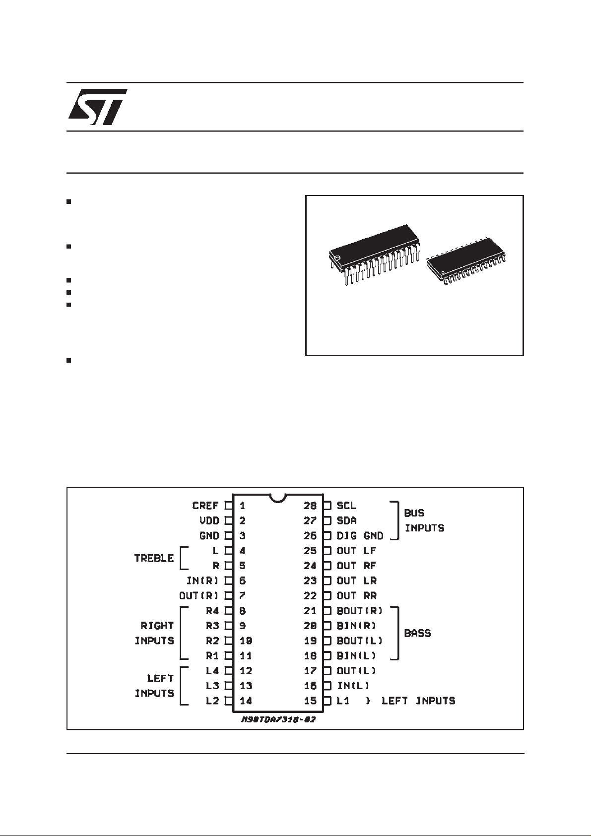
TDA7318
DIP28 SO28
ORDERING NUMBERS:
TDA7318 TDA7318D
Selectabl e input gain is provided. Control is ac co mplishedbyserialI
TheACsignalsettingisobtainedbyresistornetwo rks
andswitchescombinedwithoperationalamplifiers.
Thanks to the used BIP OLAR / C MOS Tec nol ogy ,
LowDistortion, LowNoiseandLow DC steppingare
obtained.
2
Cbusmicroprocessorinterface.
PIN CONNECTION (Topview)
November 1999
1/14

TDA7318
TEST CIRCUIT
THERMAL DATA
Symbol Description SO28 DIP28 Unit
R
thj-pins
Thermal Resistance Junction-pins max 85 65 °C/W
ABSOLUTE MAXIMUM RATINGS
Symbol Parameter Value Unit
V
T
amb
T
stg
Operating Supply Voltage 10.2 V
S
Operating Ambient Temperature -40 to 85
Storage Temperature Range -55 to +150 °C
QUICK REFERENCE DATA
Symbol Parameter Min. Typ. Max. Unit
V
V
CL
THD Total Harmonic DistortionV = 1Vrms f = 1KHz 0.01 0.1 %
S/N Signal to Noise Ratio 106 dB
S
Supply Voltage 6 9 10 V
S
Max. input signal handling 2 Vrms
Channel Separation f = 1KHz 103 dB
C
Volume Control 1.25dB step -78.75 0 dB
Bass and TrebleControl 2db step -14 +14 dB
Fader and Balance Control 1.25dBstep -38.75 0 dB
Input Gain 6.25dB step 0 18.75 dB
Mute Attenuation 100 dB
C
°
2/14

BLOCK DIAGRAM
TDA7318
BUS
C17
5.6K R2
2.7nF
C15
100nF
C14
100nF
ATT
SPKR
TREBLE(L)
4
BIN(L)
18
19
BOUT(L)
OUT
LEFT FRONT
25
RB
MUTE
ATT
SPKR
TREBLE
BASS
VOL
OUT
LEFT REAR
23
MUTE
SCL
SDA
282726
C BUS DECODER + LATCHES
2
I
DIGGND
ATT
SPKR
VOL BASS TREBLE
OUT
RIGHT FRONT
24
MUTE
ATT
SPKR
OUT
22
RB
RIGHT REAR
MUTE
TREBLE(R)
5
21 20
BOUT(R) BIN(R)
D95AU265
C13
100nF
C12
100nF
C16
2.7nF
5.6K R1
C11 2.2µF
17 16
OUT(L) IN(L)
INPUT
+ GAIN
SELECTOR
L1 15L1L2 14L2L3 13L3L4 12
4x
2.2µF
C1
C2
C3
LEFT
INPUTS
C4
L4
R4 8R4R3 9R3R2 10
C5
C6
R2
C7
RIGHT
INPUTS
11 R1
R1
C8
4x
2.2µF
SUPPLY
76
OUT(R) IN(R)
AGND CREF
V
231
C10 2.2µF
22µFC9
CC
3/14

TDA7318
ELECTRICALCHARACTERISTICS (refer tothe test circuit T
R
= 600Ω, all controlsflat (G = 0), f = 1KHz unless otherwise specified)
G
=25°C, VS= 9V,RL=10KΩ,
amb
Symbol Parameter Test Condition Min. Typ. Max. Unit
SUPPLY
V
S
I
S
SVR Ripple Rejection 60 85 dB
Supply Voltage 6 9 10 V
Supply Current 4 8 11 mA
INPUT SELECTORS
G
G
G
V
R
II
V
CL
S
IN
R
L
INmin
INmax
STEP
e
IN
DC
Input Resistance Input 1, 2, 3, 4 35 50 70 K
Clipping Level 2 2.5 Vrms
Input Separation (2) 80 100 dB
Output Load resistance pin 7, 17 2 K
Min. Input Gain -1 0 1 dB
Max. Input Gain 17 18.75 20 dB
Step Resolution 5 6.25 7.5 dB
Input Noise G = 18.75dB 2
DC Steps adjacent gain steps 4 20 mV
G = 18.75 to Mute 4 mV
VOLUMECONTROL
R
IV
C
RANGE
A
VMIN
A
VMAX
A
STEP
E
A
E
T
V
DC
Input Resistance 20 33 50 kΩ
Control Range 70 75 80 dB
Min. Attenuation -1 0 1 dB
Max. Attenuation 70 75 80 dB
Step Resolution 0.5 1.25 1.75 dB
Attenuation Set Error Av = 0 to -20dB
Av = -20 to -60dB
-1.25
-3
0 1.25
2
Tracking Error 2dB
DC Steps adjacent attenuation steps
From 0dB to Av max
0
0.5
3
7.5
SPEAKERATTENUATORS
µ
dB
dB
mV
mV
Ω
Ω
V
C
S
A
range
STEP
E
MUTE
V
DC
A
Control Range 35 37.5 40 dB
Step Resolution 0.5 1.25 1.75 dB
Attenuation set error 1.5 dB
Output Mute Attenuation 80 100 dB
DC Steps adjacent att. steps
from 0 to mute
0
1
BASS CONTROL(1)
Gb Control Range Max. Boost/cut +12 +14 +16 dB
B
STEP
R
B
Step Resolution 1 2 3 dB
Internal Feedback Resistance 34 44 58 KΩ
TREBLECONTROL(1)
Gt Control Range Max. Boost/cut +13 +14 +15 dB
Step Resolution 1 2 3 dB
4/14
T
STEP
10
3
mV
mV
TDA7318
ELECTRICALCHARACTERISTICS (continued)
Symbol Parameter Test Condition Min. Typ. Max. Unit
AUDIO OUTPUTS
V
OCL
R
L
C
L
R
OUT
V
OUT
Clipping Level d = 0.3% 2 2.5 Vrms
Output Load Resistance 2 KΩ
Output Load Capacitance 10 nF
Output resistance 30 75 120
Ω
DC Voltage Level 4.2 4.5 4.8 V
GENERAL
e
NO
S/N Signal to Noise Ratio all gains = 0dB; V
d Distortion A
Sc Channel Separation left/right 80 103 dB
Output Noise BW = 20-20KHz, flat
output muted
all gains = 0dB
A curve all gains = 0dB 3 µV
O
=0,VIN= 1Vrms
V
A
= -20dB VIN= 1Vrms
Total Tracking error A
V
= 0 to -20dB
V
V
= 0.3Vrms
IN
-20 to -60 dB
2.5
515
µV
µ
= 1Vrms 106 dB
0.01
0.09
0.04
0
0
0.1
0.3
1
2
%
%
%
dB
dB
V
BUS INPUTS
V
IL
V
IH
I
IN
V
O
Notes:
(1) Bass and Trebleresponse seeattached diagram(fig.19). The center frequencyand quality ofthe resonance behaviour can be choosen by
the external circuitry. A standard first order bass response can be realized by a standard feedback network
(2) The selected input is groundedthru the 2.2µF capacitor.
Input Low Voltage 1V
Input High Voltage 3 V
Input Current -5 +5
Output Voltage SDA
IO= 1.6mA 0.4 V
A
µ
Acknowledge
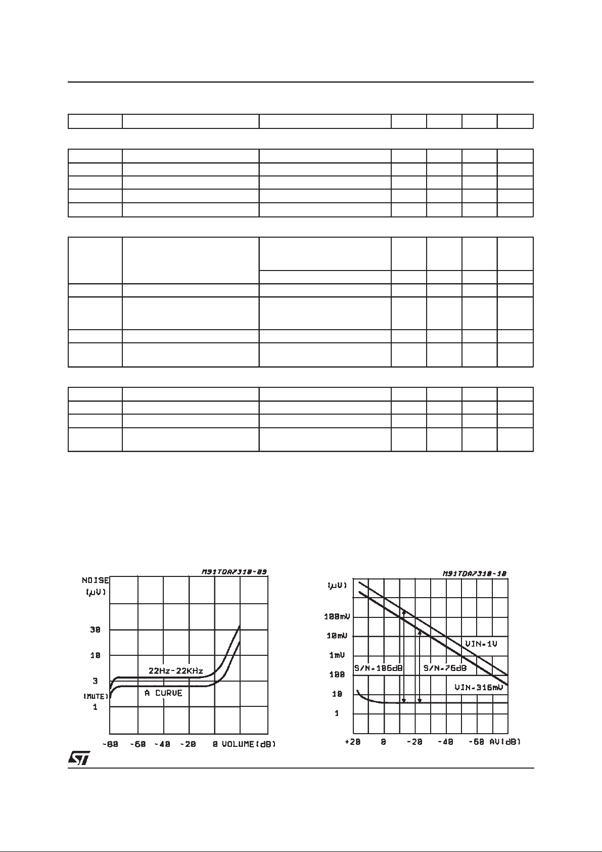
Figure 1: Noisevs. Volume/GainSettings
Figure2: Signalto Noise Ratio vs. Volume
Setting
5/14

TDA7318
Figure 3: Distortion& Noise vs. Frequency Figure4: Distortion& Noisevs. Frequency
Figure 5: Distortionvs. Load Resistance
Figure 7: InputSeparation(L1 → L2, L3, L4) vs.
Frequency
Figure6: Channel Separation (L → R) vs.
Frequency
Figure8: SupplyVoltage Rejection vs.
Frequency
6/14

TDA7318
Figure 9: OutputClipping Levelvs. Supply
Voltage
Figure 11: SupplyCurrentvs. Temperature
Figure10: QuiescentCurrent vs. Supply Voltage
Figure12: Bass Resistance vs. Temperature
Figure 13: TypicalTone Response(with the ext.
components indicatedin thetest
circuit)
7/14

TDA7318
I2C BUS INTERFACE
Data transmission from microprocessor to the
TDA7318 and viceversa takes place thru the 2
wires I
2
C BUS interface, consisting of the two
lines SDA and SCL (pull-up resistors to positive
supply voltage must be connected).
Data Validity
As shown in fig. 14, the data on the SDA line
must be stable during thehigh period of the clock.
The HIGH and LOW state of the data line can
only change when the clock signal on the SCL
line is LOW.
Start and Stop Conditions
As shown in fig.15 a start condition is a HIGH to
LOW transition of the SDA line while SCL is
HIGH. The stop condition is a LOW to HIGH transition of the SDA line while SCL is HIGH.
Byte Format
Every byte transferred on the SDA line must contain 8 bits. Each byte must be followed by an ac-
2
Figure 14: Data Validityon the I
CBUS
knowledgebit. The MSB is transferredfirst.
Acknowledge
The master(µP)putsa resistive HIGH level on the
SDA line during the acknowledgeclock pulse (see
fig. 16). The peripheral (audioprocessor) that acknowledges has to pull-down (LOW) the SDA line
during the acknowledge clock pulse, so that the
SDAlineisstableLOWduringthis clockpulse.
The audioprocessor which has been addressed
has to generate an acknowledge after the reception of each byte, otherwise the SDAline remains
at the HIGH level during the ninth clock pulse
time. In this case the master transmitter can generate the STOP information in order to abort the
transfer.
Transmissionwithout Acknowledge
Avoiding to detect the acknowledge of the audioprocessor, the µP can use a simplier transmission: simply it waits one clock without checking
the slave acknowledging, and sends the new
data.
This approach of course is less protected from
misworkingand decreasesthe noise immunity.
Figure 15: TimingDiagramof I
2
Figure 16: Acknowledgeon the I
8/14
CBUS
2
CBUS

TDA7318
SOFTWARESPECIFICATION
Interface Protocol
The interface protocol comprises:
A start condition (s)
A chip address byte, containing the TDA7318
TDA7318 ADDRESS
MSB first byte LSB MSB LSB MSB LSB
S10001000
ACK = Acknowledge
S = Start
P = Stop
MAX CLOCK SPEED 100kbits/s
ACK DATA ACK DATA ACK P
Data Transferred (N-bytes + Acknowledge)
address(the 8th bit ofthe bytemust be 0). The
TDA7318must always acknowledgeat theend
of each transmittedbyte.
A sequenceof data (N-bytes+ acknowledge)
A stopcondition (P)
SOFTWARESPECIFICATION
Chip address
1
MSB
DATA BYTES
Ax = 1.25dB steps; Bx= 10dB steps; Cx= 2dB steps; Gx = 6.25dB steps
0001000
MSB LSB FUNCTION
0
1
1
1
1
0
0
0
0
1
1
0
0
1
1
1
B2
0
1
0
1
0
1
1
B1
B1
B1
B1
B1
G1
0
1
LSB
B0
B0
B0
B0
B0
G0
C3
C3
A2
A2
A2
A2
A2
S2
C2
C2
A1
A1
A1
A1
A1
S1
C1
C1
A0
A0
A0
A0
A0
S0
C0
C0
Volume control
Speaker ATT LR
Speaker ATT RR
Speaker ATT LF
Speaker ATT RF
Audio switch
Bass control
Treble control
9/14

TDA7318
SOFTWARESPECIFICATION (continued)
DATA BYTES (detailed description)
Volume
MSB LSB FUNCTION
0 0 B2 B1 B0 A2 A1 A0 Volume 1.25dB steps
0
0
0
0
1
1
1
1
0 0 B2 B1 B0 A2 A1 A0 Volume 10dB steps
0
0
0
0
1
1
1
1
0
0
1
1
0
0
1
1
0
1
0
1
0
1
0
1
0
0
1
1
0
0
1
1
For example a volume of -45dBis given by:
00100100
0
1
0
1
0
1
0
1
0
-1.25
-2.5
-3.75
-5
-6.25
-7.5
-8.75
0
-10
-20
-30
-40
-50
-60
-70
Speaker Attenuators
MSB LSB FUNCTION
1
1
1
1
0
0
1
1
0
1
0
1
B1
B1
B1
B1
0
0
1
1
11111 Mute
B0
B0
B0
B0
0
1
0
1
A2
A2
A2
A2
0
0
0
0
1
1
1
1
A1
A1
A1
A1
0
0
1
1
0
0
1
1
A0
A0
A0
A0
0
1
0
1
0
1
0
1
Speaker LF
Speaker RF
Speaker LR
Speaker RR
For example attenuationof 25dBon speakerRF is given by:
10110100
0
-1.25
-2.5
-3.75
-5
-6.25
-7.5
-8.75
0
-10
-20
-30
10/14

Audio Switch
MSB LSB FUNCTION
0 1 0 G1 G0 S2 S1 S0 Audio Switch
0
0
0
0
1
1
1
1
0
0
1
1
0
1
0
1
0
0
1
1
0
0
1
1
0
1
0
1
0
1
0
1
Stereo 1
Stereo 2
Stereo 3
Stereo 4
Not allowed
Not allowed
Not allowed
Not allowed
+18.75dB
+12.5dB
+6.25dB
0dB
For example to select the stereo 2 input with a gain of +12.5dB the 8bit stringis:
01001001
Bass andTreble
TDA7318
0
0
1
1
1
1
0
1
C3
C3
0
0
0
0
0
0
0
0
1
1
1
1
1
1
1
1
C2
C2
0
0
0
0
1
1
1
1
1
1
1
1
0
0
0
0
C3 = Sign
For example Bass at -10dB is obtainedby the following8 bit string:
01100010
C1
C1
0
0
1
1
0
0
1
1
1
1
0
0
1
1
0
0
C0
C0
0
1
0
1
0
1
0
1
1
0
1
0
1
0
1
0
Bass
Treble
-14
-12
-10
-8
-6
-4
-2
0
0
2
4
6
8
10
12
14
11/14

TDA7318
DIM.
MIN. TYP. MAX. MIN. TYP. MAX.
A 2.65 0.104
a1 0.1 0.3 0.004 0.012
b 0.35 0.49 0.014 0.019
b1 0.23 0.32 0.009 0.013
C 0.5 0.020
c1 45° (typ.)
D 17.7 18.1 0.697 0.713
E 10 10.65 0.394 0.419
e 1.27 0.050
e3 16.51 0.65
F 7.4 7.6 0.291 0.299
L 0.4 1.27 0.016 0.050
S8°(max.)
mm inch
OUTLINE AND
MECHANICAL DATA
SO28
12/14

TDA7318
DIM.
MIN. TYP. MAX. MIN. TYP. MAX.
a1 0.63 0.025
b 0.45 0.018
b1 0.23 0.31 0.009
b2 1.27 0.050
D 37.34 1.470
E 15.2 16.68 0.598 0.657
e 2.54 0.100
e3 33.02 1.300
F 14.1 0.555
I 4.445 0.175
L 3.3 0.130
mm inch
0.012
OUTLINE AND
MECHANICAL DATA
DIP28
13/14

TDA7318
Information furnished is believed to be accurate and reliable. However, STMicroelectronics assumes no responsibility for the consequences
of use of such information nor for any infringement of patents or other rights of third parties which may result from its use. No license is
granted by implication or otherwise under any patent or patent rights of STMicroelectronics. Specification mentioned in this publication are
subject to change without notice. This publicationsupersedes and replaces all informationpreviously supplied. STMicroelectronics products
are not authorized for use as critical components in life support devices or systems without express written approval of STMicroelectronics.
The ST logo is a registered trademark of STMicroelectronics
1999STMicroelectronics – Printed in Italy– All Rights Reserved
2
C Standard Specifications as defined by Philips.
STMicroelectronics GROUP OF COMPANIES
Singapore - Spain - Sweden - Switzerland - UnitedKingdom - U.S.A.
http://www.st.com
Purchase of I
Australia - Brazil - China- Finland - France - Germany - HongKong - India - Italy - Japan - Malaysia - Malta- Morocco -
2
C Components of STMicrolectronics, conveys alicense under the Philips I2C Patent Rights to use these components in an I2C
system, provided that the systemconforms to the I
14/14
 Loading...