

TDA7316
FOURBANDSDIGITAL CONTROLLED GRAPHIC EQUALIZER
VOLUMECONTROLIN 0.375dBSTEP
FOUR BANDS STEREO GRAPHIC EQUAL-
IZER
CENTER FREQUENCY, BANDWIDTH, MAX
BOOST/CUT DEFINED BY EXTERNAL COMPONENTS
±14dB CUT/BOOSTCONTROL IN 2dB/STEP
ALL FUNCTIONS PROGRAMMABLE VIASE-
RIALBUS
VERYLOW DISTORTION
VERY LOW NOISE AND DC STEPPING BY
USE OF A MIXED BIPOLAR/CMOS TECHNOLOGY
DESCRIPTION
The TDA7316 is a monolithic, digitally controlled
graphicequaliz errealizedin BiCMO Smixed technology. The stereosignal,beforeanyfilteri ng,canbe at-
tenuated down to -17.625dB in 0.375dB step.
All the functions can be programmed via serial
bus making easy to build aµPcontrolledsystem.
Signalpath is desi gnedfor very low noiseanddistortion.
November 1999
SO28
ORDERING NUMBER: TDA7316
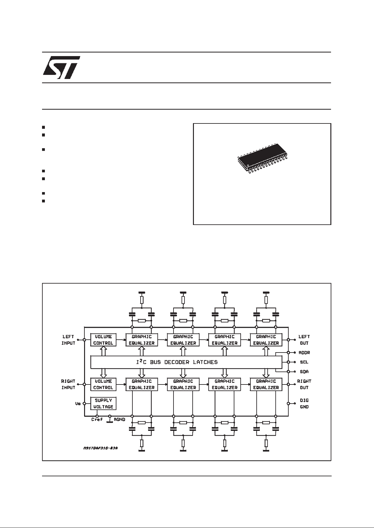
BLOCK DIAGRAM
1/10
ABSOLUTE MAXIMUM RATINGS
Symbol Parameter Value Unit
V
S
Supply Voltage 10.2 V
T
op
Operating Temperature Range -40 to +85 °C
T
stg
Storage Temperature Range -55 to +150 °C
R
tjvins
Thermal Resistance Junction pins max 85
°
C/W
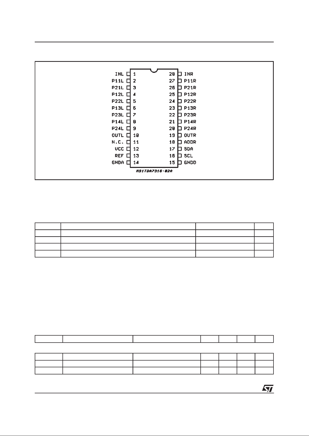
PIN CONNECTION
ELECTRICAL CHARACTERISTICS (T
amb
=25°C, VS= 9V, RL= 10KΩ,Rg= 600Ω, f = 1KHz VIN=
1Vrms, all controlsin flat position(AV = 0dB) unlessotherwise specified).
Symbol Parameter Test Condition Min. Typ. Max. Unit
SUPPLY
V
S
Supply Voltage 6 9 10 V
I
S
Supply Current 8 14 20 mA
SVR Ripple Rejection 60 80 dB
TDA7316
2/10
ELECTRICALCHARACTERISTICS (continued)
Symbol Parameter Test Condition Min. Typ. Max. Unit
INPUT
R
I
Input Resistance 20 30 40 KΩ
V
IN max
Max Input Signal THD = 0.3% 2.0 2.5 V
RMS
IN
S
Input Separation(1) 80 100 dB
VOLUMECONTROL
C
RANGE
Control Range 17.625 dB
A
VMIN
Min. Attenuation -0.5 0 0.5 dB
A
VMAX
Max. Attenuation 16.7 17.625 18.6 dB
A
STEP
Step Resolution 0.175 0.375 0.575 dB
E
A
Attenuation Set Error -1.0 1 dB
E
T
Tracking Error 0.5 dB
V
DC
DC Steps adjacent attenuation steps 0 3.0 mV
GRAPHIC EQUALIZER
THD Distortion 0.01 0.1 %
C
s
Channel Separation 80 100 dB
e
NO
Output Noise BW = 20Hz to 20KHz
flat, AV = 0dB
820µV
A curve 6
µ
V
BW = 20Hz to 20KHz AV = 0dB
All bands = max. boost
All bands = max. cut
24
6
µV
µ
V
S/N Signal to Noise Ratio A
V
= 0dB; V
ref
=1V
RMS
100 dB
B
step
Step Resolution 1 2 3 dB
C
RANGE
Control Range max boost/cut ±12 ±14 ±16 dB
VDC DC Steps Adiacent Control Steps 0.5 3 mV
AUDIO OUTPUTS
V
O
Output Voltage 2 2.5 V
RMS
R
L
Output LoadResistance 2 KΩ
C
L
Output LoadCapacitance 10 nF
R
O
Output Resistance 5 10 20
Ω
V
OUT
DC Voltage Level 4.2 4.5 4.8 V
BUS INPUTS
V
IL
Input Low Voltage 1V
V
IH
Input High Voltage 3 V
I
IN
Input Current -5 +5
µ
A
V
O
Output VoltageSDA
Acknowledge
IO= 1.6mA 0.4 V
ADDRESSPIN (Internal 50KΩ pull down resistor)
V
IL
Input Low Voltage 1V
V
IH
Input High Voltage VCC-1V V
NOTE1: The selected input is grounded thre the 2.2µF capacitor
TDA7316
3/10
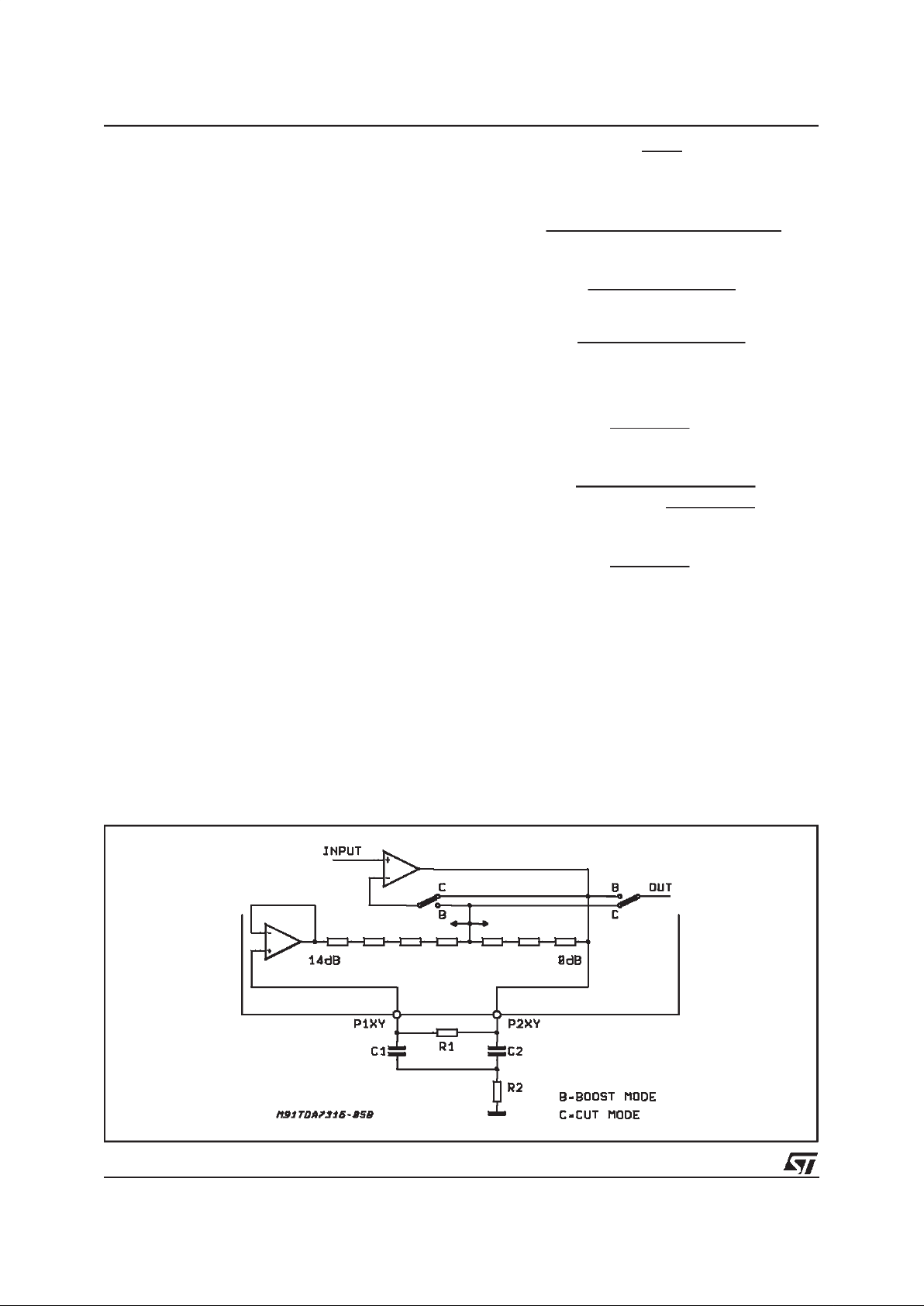
Fig. 1
x = bandnumber
y = left or right
DEVICEDESCRIPTION
The TDA7316 is a four bands, digitally controlled
stereo GraphicEqualizer.
The device is intended for high quality audio application in Hi-Fi, TV and car radio systemswhere
feature like low noise and THD are key factors. A
mixed Bipolar Cmos Technologyallows:
Cmos analog switches for pop free commutations, high frequency op.amp. (GWB = 10MHz)
and high linearity polisilicon resistor for THD =
0.01 (at Vin = 1Vrms)and a S/N ratioof 102dB.
The internalBlock Diagramis shown on page 1.
The first stage is a volume control. The control
range is 0 to -17.625dBwith 0.375dBstep.
The very high resolution (0.375dB step) allows
the implementation of closed loop amplitude control system completely free from any acustical effect (steppingvariation and pumpingeffect).
The volume control is followed by a serial four
bands equalizer. Each filtering cell is the biquad
cell shownin fig. 1
The internal resistor string is fixing the boost/cut
value while the buffer makes the Q (qualityfactor)
and central frequency, set by external components, fullyindipendentfrom the internalresistors.
Each filtering cell is realized using only 4 external
components (2 capacitorsand 2 resistors)allowing a flexible selection of centre frequency fo, Q
factor and gain. Here below the basic formulae
and the key features of each band pass filter are
reported:
f
o
= centerfrequency
Gv = gain/lossat the centerfrequencyf
o
Gv = 20log(Av)
Q
=
f
o
f2− f
1
wheref2,f1= 3dBBandwidth limits.
A
v
=
(R2⋅C2)+(R2⋅C1)
+ (R1⋅
C1
)
(R2 ⋅ C1 )+(R2 ⋅ C2 )
Q
=
√(R1
⋅ C1 ⋅ R2 ⋅ C2 )
(R2 ⋅C1 )+(R2 ⋅ C2 )
f
o
=
1
2π ⋅√(R1 ⋅ R2 ⋅
C1⋅ C2)
If C1 is fixed,then:
C2
=
Q
2
A
v
− 1− Q
2
⋅ C1
R2 =
1
2
π⋅C1⋅
f
o
⋅
(A
v
−1 ) ⋅ Q
(
A
v
− 1 −Q2)
R1
=
(A
v
− 1)
2
Av− 1 − Q
2
⋅
R2
Likewise, the components values can be determined byfixing one of the other three parameters.
Referring to fig. 1 the suggestedR2 value should
be higher than 2KΩin order to have a good THD
(internalop. amp. currentlimit).
Viceversa the R1 value should be equal or lower
than 51KΩ in order to keep the ”click”(DC step)
very low.
A typicalapplicationis shown byfig. 2
TDA7316
4/10
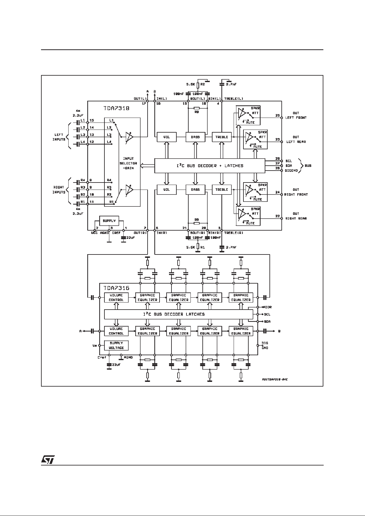
Figure 2: ApplicationCircuit
A five bands graphicequalizer is implemented using the 4 bands of the TDA7316 plus a fifth band
obtained from the bass control circuit of the
TDA7318 (or another audioprocessorof the SGSTHOMSON 731X family). Applications requiring
higher number of external equalizer bands could
be implemented by cascading 2 or more
TDA7316 devices. In fact the dedicated ADDR
pin allows 2 addressesselection. Anyway, the ad-
dress of the graphic equalizer is different from the
audioprocessorone.
For example, 9 bands are implemented by using
of 2 TDA7316 plus an audioprocessor(TDA731X
family).
In case one filteringcell is not needed,a short circuit must be provided between the P1xy and
P2xypins.
TDA7316
5/10

I2C BUS INTERFACE
Data transmission from microprocessor to the
TDA7316 and viceversa takes place thru the 2
wires I
2
C BUS interface, consisting of the two
lines SDA and SCL (pull-up resistors to positive
supply voltage must be externallyconnected).
Data Validity
As shown in fig. 3, the data on the SDA line must
be stable during the high period of theclock. The
HIGH and LOW state of the data line can only
change when the clock signal on the SCL line is
LOW.
Start and Stop Conditions
As shown in fig.4 a start condition is a HIGH to
LOW transition of the SDA line while SCL is
HIGH. The stop condition is a LOW to HIGH transition of the SDAline while SCL is HIGH.
Byte Format
Every byte transferred to the SDA line must contain 8 bits. Each byte must be followed by an acknowledgebit. The MSB is transferredfirst.
Acknowledge
The master(µP) puts a resistiveHIGH levelon the
SDA line during the acknowledge clock pulse (see
fig. 5). The peripheral (audioprocessor) that acknowledgeshas to pull-down (LOW) the SDA line
during the acknowledge clock pulse, so that the
SDAlineisstableLOWduringthis clock pulse.
The audioprocessor which has been addressed
has to generate an acknowledge after the reception of each byte, otherwise the SDA line remains
at the HIGH level during the ninth clock pulse
time. In this case the master transmitter can generate the STOP information in order to abort the
transfer.
Transmissionwithout Acknowledge
Avoiding to detect the acknowledge of the audioprocessor, the µP can use a simplier transmission: simply it generates the 9th clock pulse without checking the slave acknowledging, and then
sendsthe new data.
This approach of course is less protected from
misworkingand decreasesthe noise immunity.
Figure 3: Data Validityon the I
2
CBUS
Figure 4: TimingDiagram of I
2
CBUS
Figure 5: Acknowledgeon the I
2
CBUS
TDA7316
6/10
SOFTWARESPECIFICATION
Interface Protocol
The interfaceprotocol comprises:
A startcondition (s)
A chip address byte, containing the TDA7316
address(the 8th bit of the byte must be 0). The
TDA7316must always acknowledgeat the end
of each transmittedbyte.
A sequenceof data (N-bytes+ acknowledge)
A stopcondition (P)
TDA7316 ADDRESS
MSB first byte LSB MSB LSB MSB LSB
S100001A0
ACK
DATA
ACK
DATA
ACK
P
Data Transferred (N-bytes + Acknowledge)
ACK = Acknowledge
S = Start
P = Stop
MAX CLOCK SPEED 100kbits/s
SOFTWARESPECIFICATION
Chip address(84 or 86 Hex)
1
MSB
00001A0
LSB
A = Logic levelon pin ADDR
A = 1 if ADDR pin = open
A = 0 if ADDR pin = connectedto ground
SOFTWARESPECIFICATION (continued)
DATA BYTES(detailed description)
Volume
MSB LSB FUNCTION
0 X B2 B1 B0 A2 A1 A0 Volume 0.375dB steps
0
0
0
0
1
1
1
1
0
0
1
1
0
0
1
1
0
1
0
1
0
1
0
1
0
-0.375
-0.75
-1.125
-1.5
-1.875
-2.25
-2.625
0 X B2 B1 B0 A2 A1 A0 Volume -3dB steps
0
0
0
0
1
1
0
0
1
1
0
0
0
1
0
1
0
1
0
-3
-6
-9
-12
-15
TDA7316
7/10

Graphic Equalizer
MSB LSB FUNCTION
1 D3D2D1D0S2C1C0
0
0
0
1
0
1
1
0
1
0
1
0
Band 1
Band 2
Band 3
Band 4
D3
D3
D2
D2
D1
D1
1
0
C2
C2
C1
C1
C0
C0
cut
Boost
0
0
0
0
1
1
1
1
0
0
1
1
0
0
1
1
0
1
0
1
0
1
0
1
0dB
2dB
4dB
6dB
8dB
10dB
12dB
14dB
AX = 0.375dBsteps, BX = 3dB steps, CX = 2dB steps,X = dont’care
STATUS AFTER POWER-ON RESET
Volume -17.25dB
Graphic equalizer bands -12dB
TDA7316
8/10

SO28
DIM.
mm inch
MIN. TYP. MAX. MIN. TYP. MAX.
A 2.65 0.104
a1 0.1 0.3 0.004 0.012
b 0.35 0.49 0.014 0.019
b1 0.23 0.32 0.009 0.013
C 0.5 0.020
c1 45° (typ.)
D 17.7 18.1 0.697 0.713
E 10 10.65 0.394 0.419
e 1.27 0.050
e3 16.51 0.65
F 7.4 7.6 0.291 0.299
L 0.4 1.27 0.016 0.050
S8°(max.)
OUTLINE AND
MECHANICAL DATA
TDA7316
9/10

Information furnished is believed to be accurate and reliable. However, STMicroelectronics assumes no responsibility for the consequences
of use of such information nor for any infringement of patents or other rights of third parties which may result from its use. No license is
granted by implication or otherwise under any patent or patent rights of STMicroelectronics. Specification mentioned in this publication are
subject to change without notice. This publication supersedes and replaces all information previously supplied. STMicroelectronics products
are not authorized for use as critical components in life support devices or systems without express writtenapproval of STMicroelectronics.
The ST logois a registeredtrademark of STMicroelectronics
1999 STMicroelectronics – Printedin Italy – All Rights Reserved
Purchase of I
2
C Components of STMicrolectronics, conveys a licenseunder the Philips I2C Patent Rights to use these components in an I2C
system, provided thatthe system conforms to the I
2
C Standard Specifications as defined by Philips.
STMicroelectronics GROUP OF COMPANIES
Australia - Brazil- China- Finland - France - Germany- Hong Kong - India - Italy - Japan - Malaysia - Malta- Morocco -
Singapore- Spain- Sweden - Switzerland - UnitedKingdom - U.S.A.
http://www.st.com
TDA7316
10/10
 Loading...