

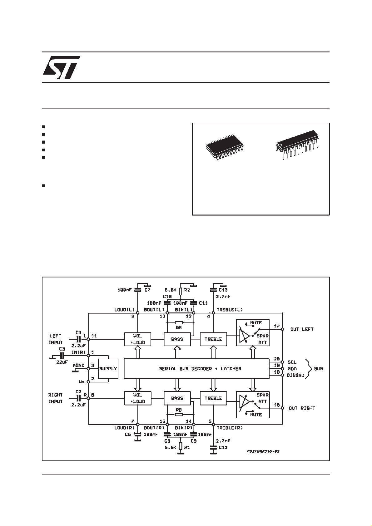
DIGITAL CONTROLLED AUDIO PROCESSOR
1 STEREOINPUT
LOUDNESSFUNCTION
VOLUMECONTROLIN 1.25dB STEPS
TREBLEAND BASSCONTROL
TWOSPEAKERSATTENUATORS:
- INDEPENDENTSPEAKERSCONTROL
IN 1.25dB STEPS
- INDEPENDENTMUTE FUNCTION
ALL FUNCTIONS PROGRAMMABLE VIA SERIAL BUS
DESCRIPTION
The TDA 7315 is a volume, tone (bass and treble)
balance(Left/Right)processorforqualityaudioapplicationsincarradioandHi-Fisystems.
Controlisaccomplishedbyserial busmicroprocessor
interface.
TheAC signalsettingis obtainedbyresistornetworks
TDA7315
SO20
ORDERING NUMBER: TDA7315 (DIP20)
and switc hes com bined with operational amplifiers.
Thanks to the used BIPOLAR /C M OS Technol ogy,
LowDistortion, Low Noiseand DC steppingare obtained.
DIP 20
TDA7315D (SO 20)
BLOCK DIAGRAM
July 1998
1/12
TDA7315
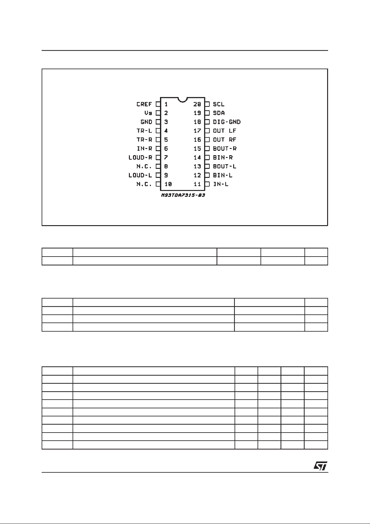
PIN CONNECTION (Topview)
THERMAL DATA
Symbol Parameter SO 20 DIP 20 Unit
R
thj-pins
Thermal Resistance Junction-pins Max. 150 150 °C/W
ABSOLUTE MAXIMUM RATINGS
Symbol Parameter Value Unit
V
T
amb
T
stg
Operating Supply Voltage 10.2 V
S
Operating Ambient Temperature -10 to 85 °C
Storage Temperature Range -55 to +150 °C
QUICK REFERENCEDATA
Symbol Parameter Min. Typ. Max. Unit
V
V
CL
THD Total Harmonic Distortion V = 1Vrms f = 1KHz 0.01 0.1 %
S/N Signal to Noise Ratio 106 dB
S
Supply Voltage 6 9 10 V
S
Max. input signal handling 2 Vrms
Channel Separation f = 1KHz 103 dB
C
Volume Control 1.25dB step -78.75 0 dB
Bass and TrebleControl 2db step -14 +14 dB
Balance Control 1.25dB step -38.75 0 dB
Mute Attenuation 100 dB
2/12
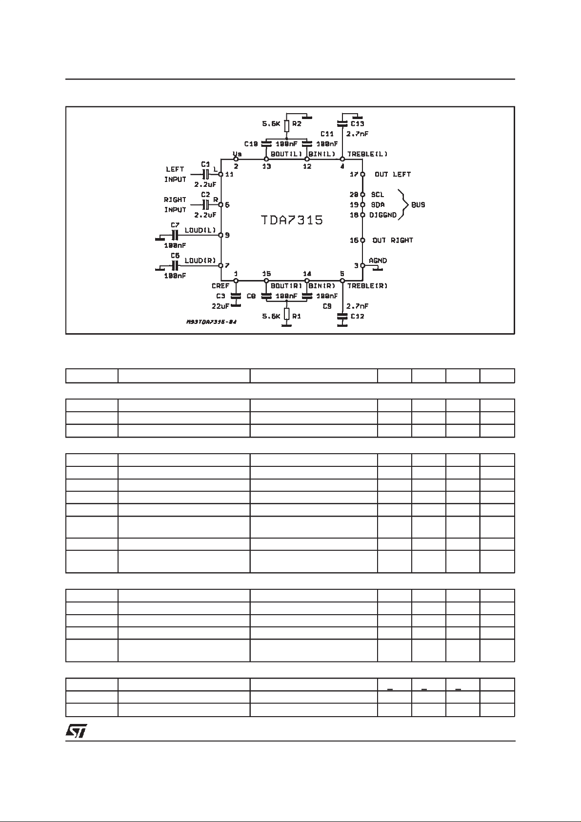
TEST CIRCUIT
TDA7315
ELECTRICAL CHARACTERISTICS (refer to the test circuit T
=25°C, VS= 9V, RL= 10KΩ,RG=
amb
600Ω, all controls flat (G = 0), f = 1KHz unless otherwisespecified)
Symbol Parameter Test Condition Min. Typ. Max. Unit
SUPPLY
V
S
I
S
SVR Ripple Rejection 60 80 dB
Supply Voltage 6 9 10 V
Supply Current 8 11 mA
VOLUMECONTROL
R
IV
C
RANGE
A
VMIN
A
VMAX
A
STEP
E
A
E
T
V
DC
Input Resistance 20 33 50 k
Control Range 70 75 80 dB
Min. Attenuation -1 0 1 dB
Max. Attenuation 70 75 80 dB
Step Resolution 0.5 1.25 1.75 dB
Attenuation Set Error Av = 0to -20dB
Av = -20to -60dB
-1.25
-3
0 1.25
2
Tracking Error 2dB
DC Steps adjacent attenuation steps
From 0dB to Av max
0
0.5
3
7.5
SPEAKERATTENUATORS
C
S
A
range
STEP
E
MUTE
V
DC
A
Control Range 35 37.5 40 dB
Step Resolution 0.5 1.25 1.75 dB
Attenuation set error 1.5 dB
Output Mute Attenuation 80 100 dB
DC Steps adjacent att. steps
from 0 to mute
0
1
3
10
BASS CONTROL (1)
Gb ControlRange Max. Boost/cut +12 +14 +16 dB
B
STEP
R
B
Step Resolution 1 2 3 dB
Internal Feedback Resistance 34 44 58 KΩ
Ω
dB
dB
mV
mV
mV
mV
3/12
TDA7315
ELECTRICALCHARACTERISTICS (continued)
Symbol Parameter Test Condition Min. Typ. Max. Unit
TREBLECONTROL (1)
Gt ControlRange Max. Boost/cut +13 +14 +15 dB
T
STEP
AUDIO OUTPUTS
Step Resolution 1 2 3 dB
V
OCL
R
L
C
L
R
OUT
V
OUT
Clipping Level d = 0.3% 2 2.5 Vrms
Output LoadResistance 2 KΩ
Output LoadCapacitance 10 nF
Output resistance 30 75 120 Ω
DC Voltage Level 4.2 4.5 4.8 V
GENERAL
e
NO
S/N Signal to Noise Ratio all gains = 0dB; V
d Distortion A
Sc Channel Separation left/right 80 103 dB
Output Noise BW = 20-20KHz, flat
output muted
all gains = 0dB
A curve all gains = 0dB 3 µV
O
=0,VIN= 1Vrms
V
A
= -20dB VIN= 1Vrms
Total Tracking error A
V
= 0 to -20dB
V
V
= 0.3Vrms
IN
-20 to -60 dB
2.5
515
µ
µV
= 1Vrms 106 dB
0.01
0.09
0.04
0
0
0.1
0.3
1
2
%
%
%
dB
dB
V
BUS INPUTS
V
IL
V
IH
I
IN
V
O
Note:
(1) Bass and Treble response seeattached diagram (fig.19). The center frequencyand quality of the resonance behaviour can be choosenby
the external circuitry. A standard first order bass response can be realized by a standard feedback network.
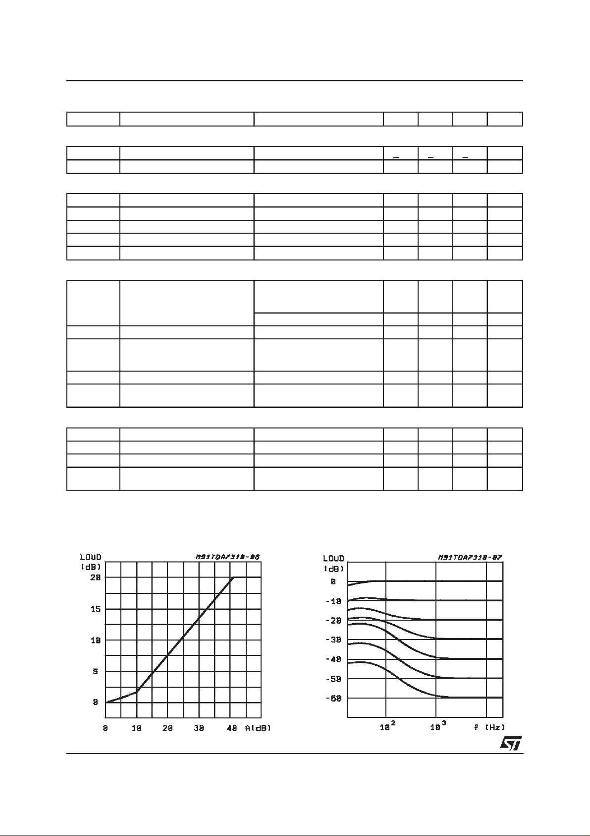
Figure 1: LoudnessversusVolume Attenuation
Input Low Voltage 1V
Input High Voltage 3 V
Input Current -5 +5 µA
Output VoltageSDA
IO= 1.6mA 0.4 V
Acknowledge
Figure2: Loudnessversus Frequency
4/12

TDA7315
Figure 3: LoudnessversusExternal Capacitors
LOUDNESS
=9V
V
S
Volume = -40dB
All other control flat
C
= 2.2µF
in
= 220nF,100nF, 33nF, 10nF, Open, Shorterto Vref
C
loud
Figure 5: Signalto Noise Ratiovs. Volume
Setting
Figure4: Noisevs. Volume/GainSettings
Figure6: Distortion& Noisevs. Frequency
Figure 7: Distortion& Noisevs. Frequency
Figure8: Distortionvs. Load Resistance
5/12

TDA7315
Figure 9: ChannelSeparation(L → R) vs.
Frequency
Figure 11: OutputClipping Level vs. Supply
Voltage
Figure10: SupplyVoltage Rejection vs.
Frequency
Figure12: QuiescentCurrent vs. SupplyVoltage
Figure 13: SupplyCurrentvs. Temperature
6/12
Figure14: BassResistance vs.Temperature

TDA7315
Figure 15: TypicalTone Response(with the ext.
components indicatedin the test
circuit)
SOFTWARE SPECIFICATION
InterfaceProtocol
The interfaceprotocol comprises:
A startcondition (S)
A chip address byte, containing the TDA7315
address(the 8th bit of the byte must be 0). The
TDA7315must always acknowledgeat the end
of each transmitted byte.
A sequenceof data (N-bytes+ acknowledge)
A stopcondition (P)
TDA7315 ADDRESS
MSB first byte LSB MSB LSB MSB LSB
S10000000
ACK
DATA
ACK
DATA
ACK
P
Data Transferred (N-bytes+ Acknowledge)
ACK = Acknowledge
S = Start
P = Stop
MAX CLOCK SPEED 100kbits/s
SOFTWARESPECIFICATION
Chip address= 80 Hex
1
MSB
DATA BYTES
Ax = 1.25dB steps; Bx= 10dB steps; Cx = 2dB steps; X = don‘t care.
0000000
MSB LSB FUNCTION
0
1
1
0
0
0
0
0
0
1
1
1
B2
0
1
0
1
1
B1
B1
B1
X
0
1
LSB
B0
B0
B0
X
C3
C3
A2
A2
A2
L
C2
C2
A1
A1
A1
X
C1
C1
A0
A0
A0
X
C0
C0
Volume control
Speaker ATT L
Speaker ATT R
Loudness
Bass control
Treble control
7/12

TDA7315
SOFTWARESPECIFICATION (continued)
DATA BYTES(detailed description)
Volume
MSB LSB FUNCTION
0 0 B2 B1 B0 A2 A1 A0 Volume 1.25dB steps
0
0
0
0
1
1
1
1
0 0 B2 B1 B0 A2 A1 A0 Volume 10dB steps
0
0
0
0
1
1
1
1
0
0
1
1
0
0
1
1
0
1
0
1
0
1
0
1
0
0
1
1
0
0
1
1
For examplea volume of -45dBis givenby:
00100100
0
1
0
1
0
1
0
1
0
-1.25
-2.5
-3.75
-5
-6.25
-7.5
-8.75
0
-10
-20
-30
-40
-50
-60
-70
Speaker Attenuators
MSB LSB FUNCTION
1
1
0
0
0
1
B1
B1
0
0
1
1
11111 Mute
B0
B0
A2
A2
0
0
0
0
1
1
1
1
0
1
0
1
A1
A1
A0
A0
0
0
1
1
0
0
1
1
0
1
0
1
0
1
0
1
Speaker L
Speaker R
For exampleattenuationof 25dBon speakerR is givenby:
10110100
0
-1.25
-2.5
-3.75
-5
-6.25
-7.5
-8.75
0
-10
-20
-30
8/12

Loudness
MSB LSB FUNCTION
010XXLXX
0
1
LOUDNESS ON
LOUDNESS OFF
x = don‘t care
For examplesLoudness Offcan be programmedby the following 8 bit string:
01000100
Bass and Treble
TDA7315
0
0
1
1
1
1
0
1
C3
C3
0
0
0
0
0
0
0
0
1
1
1
1
1
1
1
1
C2
C2
0
0
0
0
1
1
1
1
1
1
1
1
0
0
0
0
C3 = Sign
For exampleBass at -10dBis obtainedby the following8 bit string:
01100010
C1
C1
0
0
1
1
0
0
1
1
1
1
0
0
1
1
0
0
C0
C0
Bass
Treble
0
1
0
1
0
1
0
1
1
0
1
0
1
0
1
0
-14
-12
-10
-8
-6
-4
-2
0
0
2
4
6
8
10
12
14
9/12

TDA7315
SO20 PACKAGEMECHANICAL DATA
DIM.
MIN. TYP. MAX. MIN. TYP. MAX.
A 2.35 2.65 0.093 0.104
A1 0.1 0.3 0.004 0.012
B 0.33 0.51 0.013 0.020
C 0.23 0.32 0.009 0.013
D 12.6 13 0.496 0.512
E 7.4 7.6 0.291 0.299
e 1.27 0.050
H 10 10.65 0.394 0.419
h 0.25 0.75 0.010 0.030
L 0.4 1.27 0.016 0.050
K 0 (min.)8 (max.)
mm inch
L
A
B
e
K
D
1120
E
110
SO20MEC
hx45°
A1
H
C
10/12

DIP20 PACKAGE MECHANICAL DATA
TDA7315
DIM.
MIN. TYP. MAX. MIN. TYP. MAX.
a1 0.254 0.010
B 1.39 1.65 0.055 0.065
b 0.45 0.018
b1 0.25 0.010
D 25.4 1.000
E 8.5 0.335
e 2.54 0.100
e3 22.86 0.900
F 7.1 0.280
I 3.93 0.155
L 3.3 0.130
Z 1.34 0.053
mm inch
11/12

TDA7315
Information furnished is believed to be accurate and reliable. However, STMicroelectronics assumes no responsibility for the consequences
of use of such information nor for any infringement of patents or other rights of third parties which may result from its use. No license is
granted by implication or otherwise under any patent or patent rights of STMicroelectronics. Specification mentioned in this publication are
subject to change withoutnotice. This publication supersedes and replaces all information previously supplied. STMicroelectronics products
are not authorized for use as critical components in life support devices or systems without express written approval of STMicroelectronics.
The ST logo is a registeredtrademark of STMicroelectronics
1998 STMicroelectronics – Printed in Italy – All Rights Reserved
STMicroelectronics GROUP OF COMPANIES
Australia - Brazil - Canada - China - France - Germany - Italy - Japan - Korea- Malaysia - Malta - Mexico - Morocco - The Netherlands -
Singapore - Spain - Sweden - Switzerland- Taiwan- Thailand - United Kingdom - U.S.A.
12/12
 Loading...