

DIGITAL CONTROLLED STEREO AUDIO PROCESSOR
INPUTMULTIPLEXER:
- 4 STEREO INPUTS
FOURSELECTABLEADDRESSES
TWODIGITAL CONTROL OUTPUTS
INPUT AND OUTPUT FOR EXTERNAL
EQUALIZER OR NOISE REDUCTION SYSTEM
VOLUMECONTROL IN 1.25dB STEPS
TREBLEAND BASSCONTROL
TWOSPEAKER ATTENUATORS:
- INDEPENDENTSPEAKERS CONTROL
IN 1.25dB STEPS
- INDEPENDENTMUTE FUNCTION
ALL FUNCTIONS PROGRAMMABLE VIA SE-
2
RIAL I
DESCRIPTION
The TDA7312 is a volume, tone (bass and treble)
balance(Left/Right)processorforqualityaudioapplications.
C BUS
TDA7312
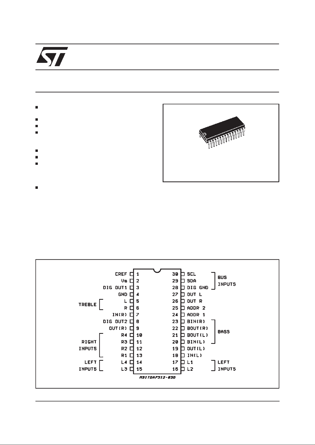
SDIP30
ORDERING NUMBER: TDA7312
Controlis accomplis hedby serialI
essorinterface.
TheAC si gnalsetti ngisobtain edbyresistornetwork s
andswitchescombinedwithoperationalamplifiers.
Thanks to the used BIPOLAR/CMOS Te cnology,
LowDistortion,Low Noise andLow DC steppingare
obtained.
2
C bus microproc-
PIN CONNECTION (Topview)
November 1999
1/13
TDA7312
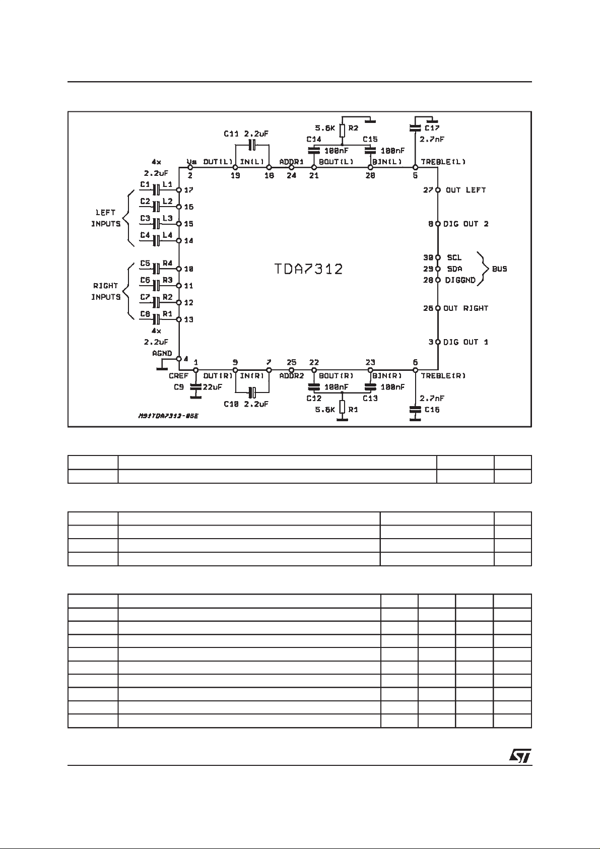
TEST CIRCUIT
THERMAL DATA
Symbol Description SDIP30 Unit
R
thj-pins
Thermal Resistance Junction-pins max 85 °C/W
ABSOLUTE MAXIMUM RATINGS
Symbol Parameter Value Unit
V
T
amb
T
stg
Operating Supply Voltage 10.2 V
S
Operating Ambient Temperature 0 to 70
Storage Temperature Range -40 to 150 °C
QUICK REFERENCE DATA
Symbol Parameter Min. Typ. Max. Unit
V
V
CL
THD Total Harmonic DistortionV = 1Vrms f = 1KHz 0.01 0.1 %
S/N Signal to Noise Ratio 106 dB
S
Supply Voltage 6 9 10 V
S
Max. input signal handling 2 Vrms
Channel Separation f = 1KHz 103 dB
C
Volume Control 1.25dB step -78.75 0 dB
Bass and TrebleControl 2db step -14 +14 dB
Fader and Balance Control 1.25dBstep -38.75 0 dB
Mute Attenuation 100 dB
C
°
2/13
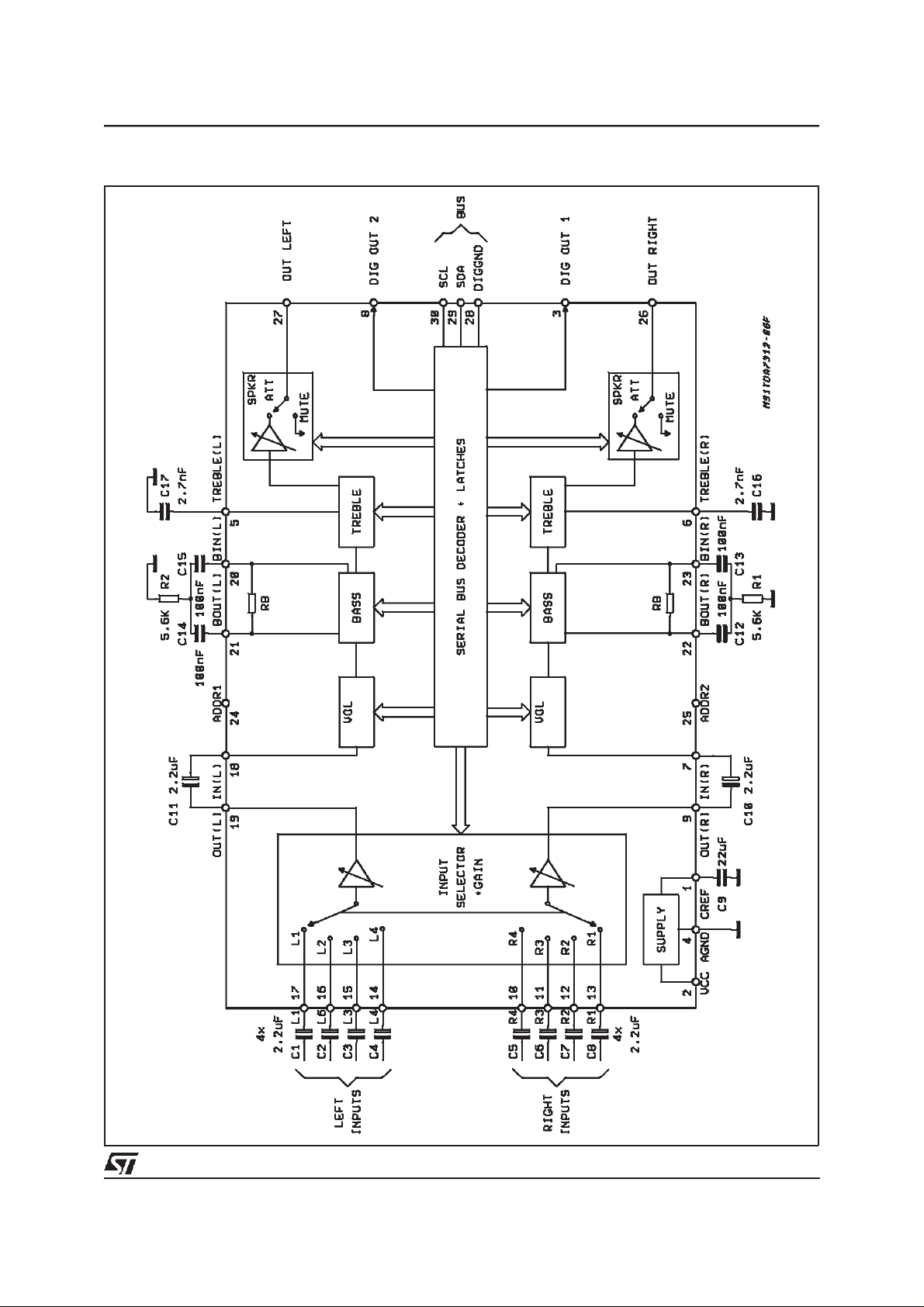
BLOCK DIAGRAM
TDA7312
3/13
TDA7312
ELECTRICALCHARACTERISTICS (refer to the test circuitT
R
= 600Ω, all controlsflat (G = 0), f =1KHz unless otherwise specified)
G
=25°C, VS= 9V,RL=10KΩ,
amb
Symbol Parameter Test Condition Min. Typ. Max. Unit
SUPPLY
V
S
I
S
SVR Ripple Rejection 60 80 dB
Supply Voltage 6 9 10 V
Supply Current 8 11 mA
INPUT SELECTORS
R
II
V
CL
S
IN
R
L
e
IN
Input Resistance Input 1, 2, 3 35 50 70 K
Clipping Level 2 2.5 Vrms
Input Separation (2) 80 100 dB
Output Load resistance 2 K
Input Noise 2
VOLUMECONTROL
R
IV
C
RANGE
A
VMIN
A
VMAX
A
STEP
E
A
E
T
V
DC
Input Resistance 20 33 50 kΩ
Control Range 70 75 80 dB
Min. Attenuation -1 0 1 dB
Max. Attenuation 70 75 80 dB
Step Resolution 0.5 1.25 1.75 dB
Attenuation Set Error Av = 0 to -20dB
Av = -20 to -60dB
-1.25
-3
0 1.25
2
Tracking Error 2dB
DC Steps adjacent attenuation steps
From 0dB to Av max
0
0.5
3
7.5
SPEAKERATTENUATORS
µ
dB
dB
mV
mV
Ω
Ω
V
C
S
A
range
STEP
E
MUTE
V
DC
A
Control Range 35 37.5 40 dB
Step Resolution 0.5 1.25 1.75 dB
Attenuation set error 1.5 dB
Output Mute Attenuation 80 100 dB
DC Steps adjacent att. steps
from 0 to mute
0
1
BASS CONTROL(1)
Gb Control Range Max. Boost/cut +12 +14 +16 dB
B
STEP
R
B
Step Resolution 1 2 3 dB
Internal Feedback Resistance 34 44 58 K
TREBLECONTROL(1)
Gt Control Range Max. Boost/cut +13 +14 +15 dB
T
STEP
Step Resolution 1 2 3 dB
DIGITALOUTPUTS
V
CESAT
I
leak
I leakage V
V
= Low IC=1mA 0.2 0.3 V
OUT
OUT=VS
3
10
mV
mV
10 µA
Ω
4/13

TDA7312
ELECTRICALCHARACTERISTICS (continued)
Symbol Parameter Test Condition Min. Typ. Max. Unit
AUDIO OUTPUTS
V
OCL
R
L
C
L
R
OUT
V
OUT
Clipping Level d = 0.3% 2 2.5 Vrms
Output Load Resistance 2 KΩ
Output Load Capacitance 10 nF
Output resistance 30 75 120
Ω
DC Voltage Level 4.2 4.5 4.8 V
GENERAL
e
NO
S/N Signal to Noise Ratio all gains = 0dB; V
d Distortion A
Sc Channel Separation left/right 80 103 dB
Output Noise BW = 20-20KHz, flat
output muted
all gains = 0dB
A curve all gains = 0dB 3 µV
O
=0,VIN= 1Vrms
V
A
= -20dB VIN= 1Vrms
Total Tracking error A
V
= 0 to -20dB
V
V
= 0.3Vrms
IN
-20 to -60 dB
2.5
515
µV
µ
= 1Vrms 106 dB
0.01
0.09
0.04
0
0
0.1
0.3
1
2
%
%
%
dB
dB
V
BUS INPUTS
V
IL
V
IH
I
IN
V
O
Input Low Voltage 1V
Input High Voltage 3 V
Input Current -5 +5
A
µ
OutputVoltageSDA Acknowledge IO= 1.6mA 0.4 V
ADDRESSPIN (Internal 50KΩ pull down resistor).
Notes:
SDA, SCL, DIG OUT 1, DIGOUT 2 Pins are high impedance when V
(1) Bass and Trebleresponse see attached diagram(fig.16). The center frequency and quality of the resonance behaviour can be choosen by
the external circuitry. A standard first order bass response can be realized by a standard feedback network
(2) The selected input is grounded thru the 2.2µF capacitor.
S
=0
Figure 1: Noisevs. Volume/GainSettings
Figure2: Signal to NoiseRatio vs. Volume
Setting
5/13

TDA7312
Figure 3: Distortion& Noisevs. Frequency Figure4: Distortion& Noise vs. Frequency
Figure 5: Distortionvs. Load Resistance
Figure 7: InputSeparation(L1 → L2, L3,L4) vs.
Frequency
Figure6: Channel Separation (L → R) vs.
Frequency
Figure8: SupplyVoltage Rejection vs.
Frequency
6/13

TDA7312
Figure 9: OutputClipping Level vs. Supply
Voltage
Figure 11: SupplyCurrent vs. Temperature
Figure10: QuiescentCurrent vs. Supply Voltage
Figure12: Bass Resistance vs. Temperature
Figure 13: TypicalTone Response (with the ext.
components indicatedin the test
circuit)
7/13

TDA7312
I2C BUS INTERFACE
Data transmission from microprocessor to the
TDA7312 and viceversa takes place thru the 2
wires I
2
C BUS interface, consisting of the two
lines SDA and SCL (pull-up resistors to positive
supply voltage must be connected).
Data Validity
As shown in fig. 14, the data on the SDA line
must be stable during the high period of the clock.
The HIGH and LOW state of the data line can
only change when the clock signal on the SCL
line is LOW.
Start and Stop Conditions
As shown in fig.15 a start condition is a HIGH to
LOW transition of the SDA line while SCL is
HIGH. The stop condition is a LOW to HIGH transition of the SDA line while SCL is HIGH.
Byte Format
Every byte transferred on the SDA line must contain 8 bits. Each byte must be followed by an ac-
2
Figure 14: Data Validityon the I
CBUS
knowledgebit. The MSB is transferredfirst.
Acknowledge
The master(µP)puts a resistive HIGHlevel on the
SDA line during the acknowledgeclock pulse(see
fig. 16). The peripheral (audioprocessor) that acknowledges has to pull-down (LOW) the SDA line
during the acknowledge clock pulse, so that the
SDAlineis stableLOWduringthis clockpulse.
The audioprocessor which has been addressed
has to generate an acknowledge after the reception of each byte, otherwise the SDAline remains
at the HIGH level during the ninth clock pulse
time. In this case the master transmitter can generate the STOP information in order to abort the
transfer.
Transmissionwithout Acknowledge
Avoiding to detect the acknowledge of the audioprocessor, the µP can use a simplier transmission: simply it waits one clock without checking
the slave acknowledging, and sends the new
data.
This approach of course is less protected from
misworkingand decreasesthe noise immunity.
Figure 15: TimingDiagram of I
2
Figure 16: Acknowledgeon the I
8/13
CBUS
2
CBUS

TDA7312
SOFTWARESPECIFICATION
Interface Protocol
The interface protocol comprises:
A start condition (s)
A chip address byte, containing the TDA7312
TDA7312 ADDRESS
MSB first byte LSB MSB LSB MSB LSB
S 1 0 0 0 1 ADDR2ADDR10
ACK = Acknowledge
S = Start
P = Stop
ACK
SOFTWARESPECIFICATION
Chip address
1
MSB
0001ADDR
DATA BYTES
ADDR10
2
LSB
address(the 8th bit of the byte must be 0).The
TDA7312must always acknowledgeat theend
of each transmittedbyte.
A sequenceof data(N-bytes + acknowledge)
A stopcondition (P)
DATA
Data Transferred (N-bytes + Acknowledge)
ADDR2 ADDR1 CHIP ADDRESS
0 0 88 HEX
0 1 8A HEX
1 0 8C HEX
1 1 8E HEX
ACK
DATA
AC K
P
MSB LSB FUNCTION
0
1
1
0
0
0
Ax = 1.25dB steps; Bx = 10dB steps; Cx = 2dB steps; Sx = Input Selector; D
0
0
0
1
1
1
B2
0
1
0
1
1
B1
B1
B1
D2
0
1
B0
B0
B0
D1
C3
C3
A2
A2
A2
S2
C2
C2
A1
A1
A1
S1
C1
C1
= Dig Out Pins
X
A0
A0
A0
S0
C0
C0
Volume control
Speaker ATT L
Speaker ATT R
Audio switch
Bass control
Treble control
9/13

TDA7312
SOFTWARESPECIFICATION(continued)
DATA BYTES (detailed description)
Volume
MSB LSB FUNCTION
0 0 B2 B1 B0 A2 A1 A0 Volume 1.25dB steps
0
0
0
0
1
1
1
1
0 0 B2 B1 B0 A2 A1 A0 Volume 10dB steps
0
0
0
0
1
1
1
1
0
0
1
1
0
0
1
1
0
1
0
1
0
1
0
1
0
0
1
1
0
0
1
1
For example a volume of -45dBis given by:
00100100
0
1
0
1
0
1
0
1
0
-1.25
-2.5
-3.75
-5
-6.25
-7.5
-8.75
0
-10
-20
-30
-40
-50
-60
-70
Speaker Attenuators
MSB LSB FUNCTION
1
1
0
0
0
1
B1
B1
0
0
1
1
11111 Mute
B0
B0
A2
A2
0
0
0
0
1
1
1
1
0
1
0
1
A1
A1
A0
A0
0
0
1
1
0
0
1
1
0
1
0
1
0
1
0
1
Speaker L
Speaker R
For example attenuationof 25dB on speakerR is given by:
10110100
0
-1.25
-2.5
-3.75
-5
-6.25
-7.5
-8.75
0
-10
-20
-30
10/13

Audio Switch
MSB LSB FUNCTION
0 1 0 D2 D1 S2 S1 S0 Audio Switch
1
1
1
1
0
1
0
1
0
0
1
1
0
1
0
1
Stereo 1
Stereo 2
Stereo 3
Stereo 4
DIG. OUT 1 = 0
DIG. OUT 1 = 1
DIG. OUT 2 = 0
DIG. OUT 2 = 1
Bass andTreble
TDA7312
0
0
1
1
1
1
0
1
C3
C3
0
0
0
0
0
0
0
0
1
1
1
1
1
1
1
1
C2
C2
0
0
0
0
1
1
1
1
1
1
1
1
0
0
0
0
C3 = Sign
For example Bass at -10dB is obtainedby the following8 bitstring:
01100010
Status at Poweron Reset
Volume= 78.75dB
Treble = Bass = +2dB
Spkrs Attenuators= Mute
Input = Stereo 1
Dig. OUT1 = Dig. OUT 2 = 1
C1
C1
0
0
1
1
0
0
1
1
1
1
0
0
1
1
0
0
C0
C0
0
1
0
1
0
1
0
1
1
0
1
0
1
0
1
0
Bass
Treble
-14
-12
-10
-8
-6
-4
-2
0
0
2
4
6
8
10
12
14
11/13

TDA7312
DIM.
MIN. TYP. MAX. MIN. TYP. MAX.
A 5.08 0.20
A1 0.51
A2 3.05 3.81 4.57 0.12 0.15 0.18
B 0.36 0.46 0.56 0.014 0.018 0.022
B1 0.76 0.99 1.40 0.030 0.039 0.055
C 0.20 0.25 0.36 0.008 0.01 0.014
D 27.43 27.94 28.45 1.08 1.10 1.12
E 10.16 10.41 11.05 0.400 0.410 0.435
E1 8.38 8.64 9.40 0.330 0.340 0.370
e 1.778 0.070
e1 10.16 0.400
L 2.54 3.30 3.81 0.10 0.13 0.15
M0°(min.),15°(max.)
S 0.31 0.012
mm inch
0.020
OUTLINE AND
MECHANICAL DATA
SDIP30 (0.400”)
12/13

TDA7312
Information furnished is believed to be accurate and reliable. However, STMicroelectronics assumes no responsibility for the consequences
of use of such information nor for any infringement of patents or other rights of third parties which may result from its use. No license is
granted by implication or otherwise under any patent or patent rights of STMicroelectronics. Specification mentioned in this publication are
subject to change without notice. This publication supersedes and replaces all information previously supplied. STMicroelectronics products
are not authorized for use as critical components in life support devices or systems without express written approval of STMicroelectronics.
The ST logo is a registered trademark of STMicroelectronics
1999STMicroelectronics – Printed in Italy – AllRights Reserved
2
Purchase of I
C Components of STMicroelectronics,conveys a license under the Philips I2C Patent Rights to use these components in an
2
C system, provided thatthe system conforms to the I2C Standard Specifications as defined by Philips.
I
Australia - Brazil - China - Finland - France - Germany- HongKong - India - Italy - Japan - Malaysia- Malta - Morocco -
Singapore - Spain - Sweden - Switzerland - United Kingdom - U.S.A.
STMicroelectronics GROUP OF COMPANIES
http://www.st.com
13/13
 Loading...