

SERIAL BUS CONTROLLED AUDIO PROCESSOR
INPUTMULTIPLEXER
– TWOSTEREODIFFERENTIAL INPUTS
– TWOSTEREOSINGLE ENDEDINPUTS
– ONE MONO DIFFERENTIAL INPUT
INPUT AND OUTPUT FOR EXTERNAL
EQUALIZER OR NOISE REDUCTION SYSTEM
VOLUMECONTROL IN 1.25dB STEPS
TREBLEAND BASS CONTROL
FOURSPEAKERATTENUATORS:
– 4 INDEPENDENTSPEAKERSCONTROL
IN 1.25dB STEPS FOR BALANCE AND
FADERFACILITIES
– INDEPENDENTMUTE FUNCTION
ALL FUNCTIONS PROGRAMMABLE VIA SPI
COMPATIBLESERIAL BUS
DESCRIPTION
The TDA7311 is a volume, tone (bass and treble)
and fader (front/rear) processor for high quality
audio applicationsin carradio and Hi-Fi systems.
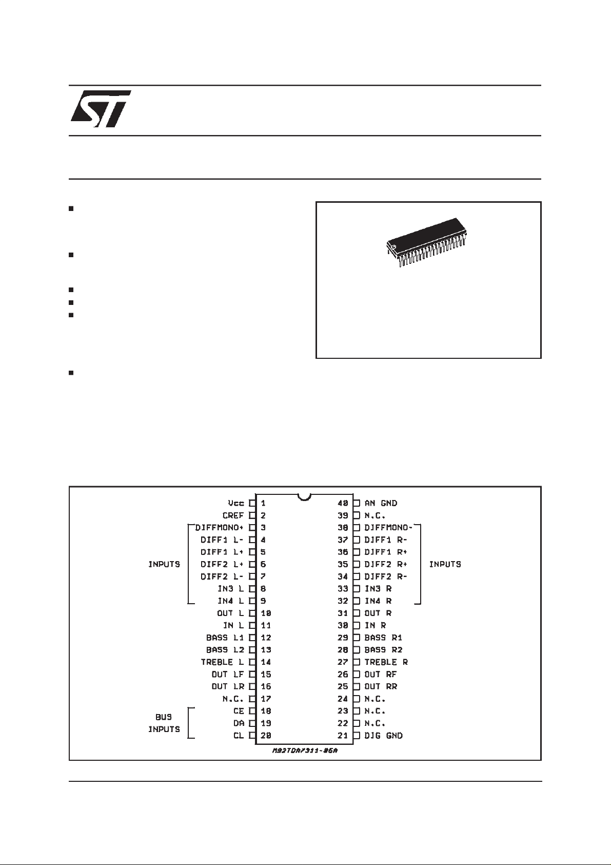
TDA7311
DIP40
ORDERING NUMBER: TDA7311
Control is accomplished by serial bus microprocessorinterface.
The AC signal setting is obtained by resistor networks and switches combined with operational
amplifiers.
Thanks to the used BIPOLAR/CMOStechnology,
low distortion, low noise and DC stepping are obtained.
PINS CONNECTION
July 1999
(Top view)
1/11
TDA7311
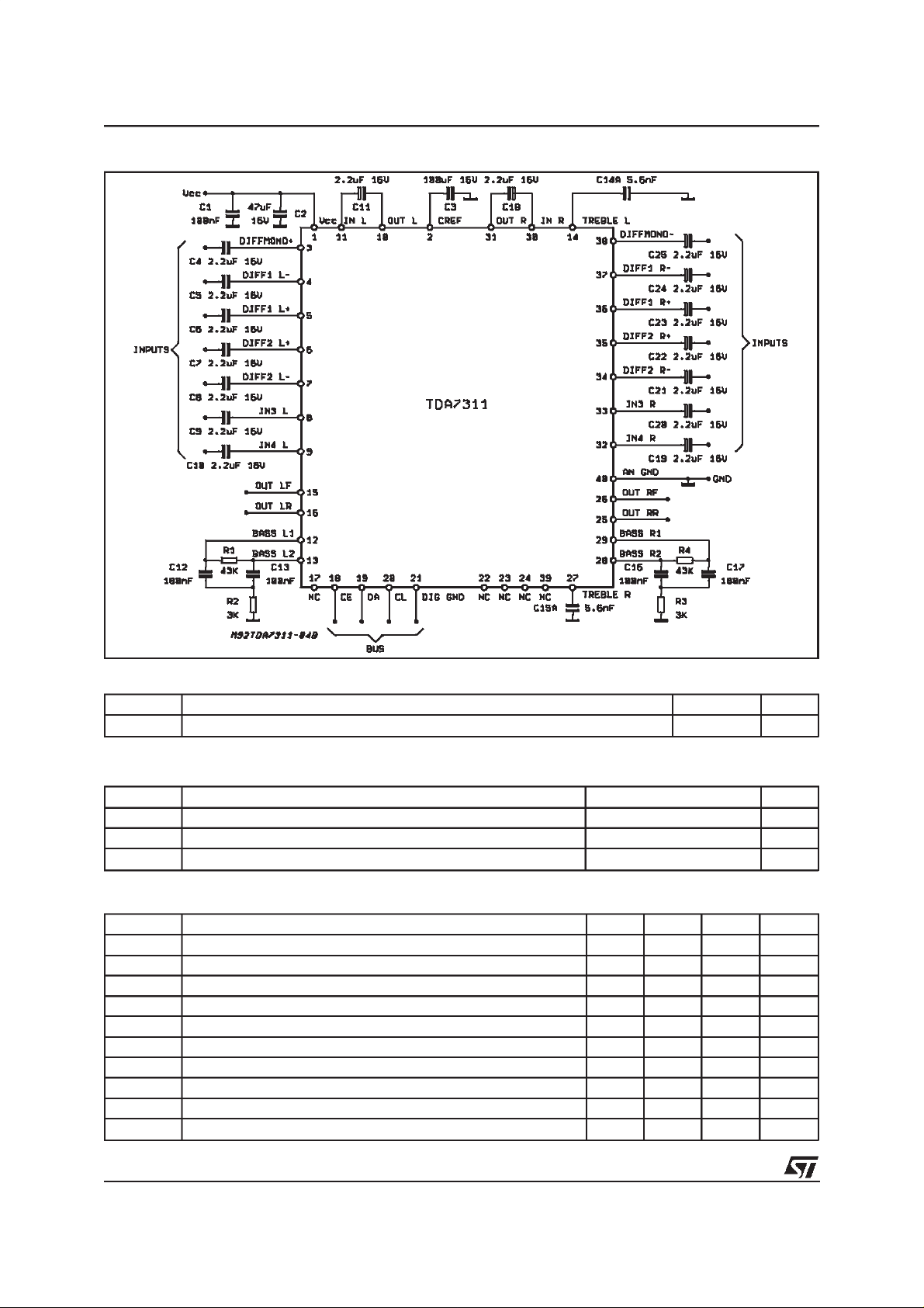
TEST CIRCUIT
THERMAL DATA
Symbol Description DIP40 Unit
R
thj-pins
Thermal Resistance Junction-pins max 85
ABSOLUTE MAXIMUM RATINGS
Symbol Parameter Value Unit
V
T
T
Operating Supply Voltage 11.2 V
S
Operating Temperature Range -40 to 85
op
Storage Temperature Range -55 to +150
stg
QUICK REFERENCE DATA
Symbol Parameter Min. Typ. Max. Unit
V
V
CL
THD Total Harmonic Distortion V = 1Vrms f = 1KHz 0.01 %
S/N Signal to Noise Ratio 106 dB
S
BR
Supply Voltage 8 10 11 V
S
Max. input signal handling 2.3 Vrms
Channel Separation f = 1KHz 95 dB
C
Volume Control 1.25dB step -78.75 +11.25 dB
Treble Control 2dB step -14 +14 dB
Bass Control 2dB step –20 +20 dB
SS
Fader and Balance Control 1.25dB step -38.75 0 dB
Mute Attenuation 92 dB
C/W
°
°
°
C
C
2/11
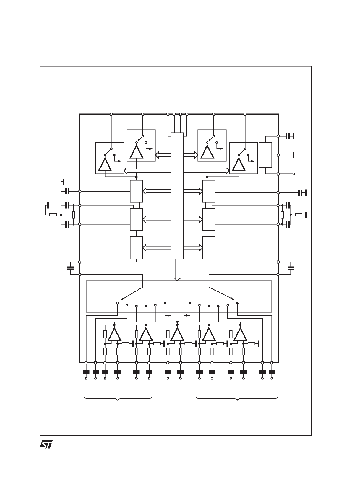
BLOCK DIAGRAM
TDA7311
ATT
SPKR
OUT
LEFT REAR
16
TREBLE
VOL BASS
MUTE
CLDACE
201918
DIG GND
21
SPI BUS DECODER + LATCHES
OUT
LEFT FRONT
15
ATT
SPKR
14
12 13
MUTE
ATT
SPKR
OUT
RIGHT FRONT
26
MUTE
VOL BASS TREBLE
ATT
SPKR
OUT
25
RIGHT REAR
MUTE
SUPPLY
1402
27
AN-GND CREF
CC
V
10 11
SECMUTE
9
8
4
IN4
IN3
DIFF
5
STEREO 1
LEFT
INPUTS
7
DIFF
6
STEREO 2
38
3
DIFF MONO
SECMUTE
34
DIFF
STEREO 2
35
37
36
DIFF
STEREO 1
RIGHT
INPUTS
31 30 29 28
33
IN3
D94AU178
32
IN4
3/11
TDA7311
ELECTRICALCHARACTERISTICS (T
=25°C,VCC= 10V, RL= 10KΩ,RG= 600Ω,GV=0dB,
amb
f = 1KHzunless otherwise specified)(referto thetest circuit)
Symbol Parameter Test Condition Min. Typ. Max. Unit
SUPPLY
V
S
I
S
SVR Ripple Rejection 55 80 dB
Supply Voltage 8 10 11 V
Supply Current 15 20 mA
INPUT SELECTORS
R
II
V
CL
CMRR Common Mode Rejection Differential Inputs 65 dB
INS Input Separation (2) 70 90 dB
R
L
C
L
R
O
G
IN
Input Resistance Single Ended inputs 30 50 70 K
Differential Inputs 10 20 KΩ
Clipping Level Single Ended Inputs 2.3 2.8 Vrms
Differential Inputs 4.6 5.6 Vrms
Output Load resistance 2 K
Output Load capacitance 1 nF
Output Impedance 15 50 Ω
Input Gain Single Ended Inputs -1 0 1 dB
differential Inputs -7 -6 -5 dB
VOLUMECONTROL
Ω
Ω
R
IN
G
R
Input Resistance 15 30 k
Control Range Max. Attenuation – 75 dB
Max. Gain +11.25 dB
A
STEP
E
A
E
T
V
DC
Step Resolution 1.25 dB
Attenuation Set Error AV= +11.25 to -20dB
A
= -20 to -60dB
V
-1.25
-3
0 1.25
2
Tracking Error 2dB
DC Steps adjacent attenuationsteps
From 0dB to A
Vmax
0
1
3.0
10.0mVmV
Vimax. Max. Input Voltage 2.3 2.8 Vrms
SPEAKERATTENUATORS
A
R
A
step
E
A
V
DC
Control Range 37.5 dB
Step Resolution 1.25 dB
Attenuation set error 1.5 dB
DC Steps adjacent att.steps
from 0 to mute
0
1
BASS CONTROL(1)
Control Range +20 dB
Step Resolution 2 dB
Attenuation / Gain set error –2.0 2.0 dB
TREBLECONTROL(1)
Ω
dB
dB
mV
mV
4/11
Control Range +14 dB
Step Resolution 2.0 dB
Attenuation / Gain set error –1.0 0 1.0 dB

TDA7311
ELECTRICALCHARACTERISTICS (continued)
Symbol Parameter Test Condition Min. Typ. Max. Unit
AUDIO OUTPUTS
Output Voltage d = 0.3% 2.3 2.8 Vrms
Output Load Resistance 2 KΩ
Output Load Capacitance 10 nF
Output resistance 25 75
DC Voltage Level 4.6 5.0 5.4 V
GENERAL
Ω
e
NO
S/N Signal to Noise Ratio all gains = 0dB; V
d Distortion V
Output Noise BW = 20-20KHz, flat
output muted
all gains = 0dB Single Ended
all gains = 0dB Diff. Inputs
O
Single Ended
DifferentialInputs
= 1Vrms 0.01 %
IN
= 1Vrms
4
5
10
106
100
15
30
µ
µ
µV
dB
dB
V
V
Sc Channel Separation left/right 70 95 dB
Total Tracking error A
= 0 to -20dB
V
A
= -20 to -60 dB
V
A
= 0dB to 11.25dB
V
0
0
0
1
2
1
dB
dB
dB
Output Attenuation MuteCondition (3) 80 90 dB
BUS INPUTS
V
IL
V
IH
Notes:
(1) Bass and Trebleresponse see attached diagram (fig.17). The center frequency and quality of the resonance behaviour can be choosen by
the external circuitry. A standard first order bass response can be realized by a standard feedback network
(2) The selected input is groundedthru the 2.2µF capacitor.
(3) Condition obtained programming: mute on speaker attenuators (1X111111) followed by selection of SECMUTE (1XXXX111).
Input Low Voltage 1V
Input High Voltage 3 V
5/11

TDA7311
APPLICATIONINFORMATION
SERIALBUS INTERFACE
The serial bus interface is compatible to SPI bus
systems.
During the LOW state of the chip enable signal
(CE) the data on pin DA are clocked into the shift
register at the LOW to HIGH transition of the
clock signal CL.
At the LOW to HIGH transition of the CE signal
the content of the internal shift register is stored
into the addressedlatches.
Figure 1:
BUSTiming
The transmissionis separatedinto byteswith 8 bit
according to the data specification of the audioprocessor. After every byte a positive slope of the
CE signal has to be generated in order to store
the data byte.
A special clock counter enables the latch of the
data byte only, if exactly 8 clocks were present
during the LOW state of the CE signal. This results in a high immunity against spikes on the
clock line and avoids a storage of wrong databytes.
Nr. Parameter Min. Max. Units
Clock Frequency 250 KHz
1 CE Lead time 4 µs
2 Clock High Time 2
3 Clock Low Time 2
4 Data Hold Time 1.8 µs
5 Data Setup Time 1.8
6 Clock Setup Time 0
7 CE lagtime 0
8 Clock Hold Time 6 µs
9 CE High TIme 6
6/11
s
µ
s
µ
s
µ
s
µ
s
µ
s
µ

STATUSAFTER POWER-ONRESET
Volume –78.75dB
Speaker Mute
Audio Switch Mute
Bass –20dB
Treble –14dB
SOFTWARESPECIFICATION
Data Bytes
FIRST BYTE
MSB LSB Function
0 0 0 0 X X X X VOL ATTENUATION
0 1 0 0 X X X X VOL GAIN
0 0 1 0 X X X X BASS
0 1 1 0 X X X X TREBLE
0 0 0 1 X X X X ATT RF (speaker)
0 1 0 1 X X X X ATT RR (speaker)
0 0 1 1 X X X X ATT LF (speaker)
0 1 1 1 0 X X X ATT LR (speaker)
0 1 1 1 1 X X X AUDIO SWITCH
TDA7311
SECONDBYTE
VOLUMEATTENUATION
MSB LSB
1 X B2 B1 B0 A2 A1 A0 Volume 1.25dB Steps
0
0
0
0
0
0
1
0
1
0
0
1
0
1
1
1
1
1
1 X B2 B1 B0 Volume 10dB Steps
0
0
0
0
0
0
1
1
1
1
1
0
0
1
1
1
0
0
1
0
0
1
1
1
-1.25
1
-2.5
0
-3.75
1
-5.00
0
-6.25
1
-7.50
0
-8.75
1
0
-10
-20
-30
-40
-50
-60
-70
7/11
TDA7311
SOFTWARESPECIFICATION (continued)
VOLUMEGAIN
MSB LSB 1.25dB STEPS
1 X X X 0 0 0 0 0.00
1 X X X 0 0 0 1 1.25
1 X X X 0 0 1 0 2.50
1 X X X 0 0 1 1 3.75
1 X X X 0 1 0 0 5.00
1 X X X 0 1 0 1 6.25
1 X X X 0 1 1 0 7.50
1 X X X 0 1 1 1 8.75
1 X X X 1 0 0 0 10.00
1 X X X 1 0 0 1 11.25
SPEAKERATTENUATION
MSB LSB 1.25dB STEPS
10000
1 0 0 1 -1.25
1 0 1 0 -2.50
1 0 1 1 -3.75
1 1 0 0 -5.00
1 1 0 1 -6.25
1 1 1 0 -7.50
1 1 1 1 -8.75
10dB STEPS
1X000 0
1X001 -10
1X010 -20
1X011 -30
1X111111 MUTE
AUDIO SWITCH
MSB LSB INPUT
1 X X X X 0 0 0 MONO
1 X X X X 0 0 1 DIFF1
1 X X X X 0 1 0 DIFF2
1XXXX011IN3
1XXXX100IN4
1 X X X X 1 1 1 SECMUTE
8/11

SOFTWARESPECIFICATION (continued)
TREBLE
MSB LSB 2dB STEPS
1XXX0111 14
1XXX0110 12
1XXX0101 10
1XXX0100 8
1XXX0011 6
1XXX0010 4
1XXX0001 2
1XXX0000 0
1XXX1000 -0
1XXX1001 -2
1XXX1010 -4
1XXX1011 -6
1XXX1100 -8
1XXX1101 -10
1XXX1110 -12
1XXX1111 -14
BASS
TDA7311
MSB LSB 2dB STEPS
1XX11111 -20
1XX11001 -18
1XX11000 -16
1XX10111 -14
1XX10110 -12
1XX10101 -10
1XX10100 -8
1XX10011 -6
1XX10010 -4
1XX10001 -2
1XX10000 0
1XX00000 0
1XX00001 2
1XX00010 4
1XX00011 6
1XX00100 8
1XX00101 10
1XX00110 12
1XX00111 14
1XX01000 16
1XX01001 18
1XX01111 20
9/11

TDA7311
DIM.
MIN TYP MAX MIN TYP MAX
a1 0.63 0.025
b 0.45 0.018
b1 0.23 0.31 0.009
b2 1.27 0.050
D 52.58 2.070
E 15.2 16.68 0.598 0.657
e 2.54 0.100
e3 48.26 1.900
F 14.1 0.555
I 4.445 0.175
L 3.3 0.130
mm inch
0.012
OUTLINE AND
MECHANICAL DATA
DIP40
10/11

TDA7311
Information furnished is believed to be accurate and reliable. However, STMicroelectronics assumes no responsibility for the consequences
of use of such information nor for any infringement of patents or other rights of third parties which may result from its use. No license is
granted by implication or otherwise under any patent or patent rights of STMicroelectronics. Specification mentioned in this publication are
subject to change without notice. This publication supersedes and replaces all information previously supplied. STMicroelectronics products
are not authorized for use as critical components in life support devices or systems without express written approval of STMicroelectronics.
The ST logo is a registered trademark of STMicroelectronics
1999STMicroelectronics – Printed in Italy – All Rights Reserved
STMicroelectronics GROUP OF COMPANIES
Australia - Brazil - China - Finland - France - Germany - Hong Kong - India - Italy - Japan - Malaysia - Malta - Morocco -
Singapore - Spain - Sweden - Switzerland - United Kingdom - U.S.A.
http://www.st.com
11/11
 Loading...