

DIGITAL CONTROLLEDSTEREO AUDIO PROCESSOR
INPUTMULTIPLEXER:
3 STEREOINPUTS
RECORDOUTPUTFUNCTION
LOUDNESSFUNCTION
VOLUMECONTROL IN 1dB STEPS
INDEPENDENT LEFT AND RIGHT VOLUME
CONTROL
SOFTMUTEFUNCTION
ALL FUNCTIONS PROGRAMMABLE VIA SE-
2
RIAL I
DESCRIPTION
The TDA7309 is a control processor with independent left and right volume control for quality
audio applications. Selectable external loudness
and softmute functions are provided.
Control is accomplished by serial I
processorinterface.
The AC signal setting is obtained by resistor net-
C BUS
2
C bus micro-
TDA7309
WITH LOUDNESS
DIP20 SO20
ORDERING NUMBER:
TDA7309 TDA7309D
works and switches combined with operational
amplifiers.
Thanks to the used BIPOLAR/CMOSTechnology,
Low Distortion, Low Noise and Low DC stepping
are obtained.
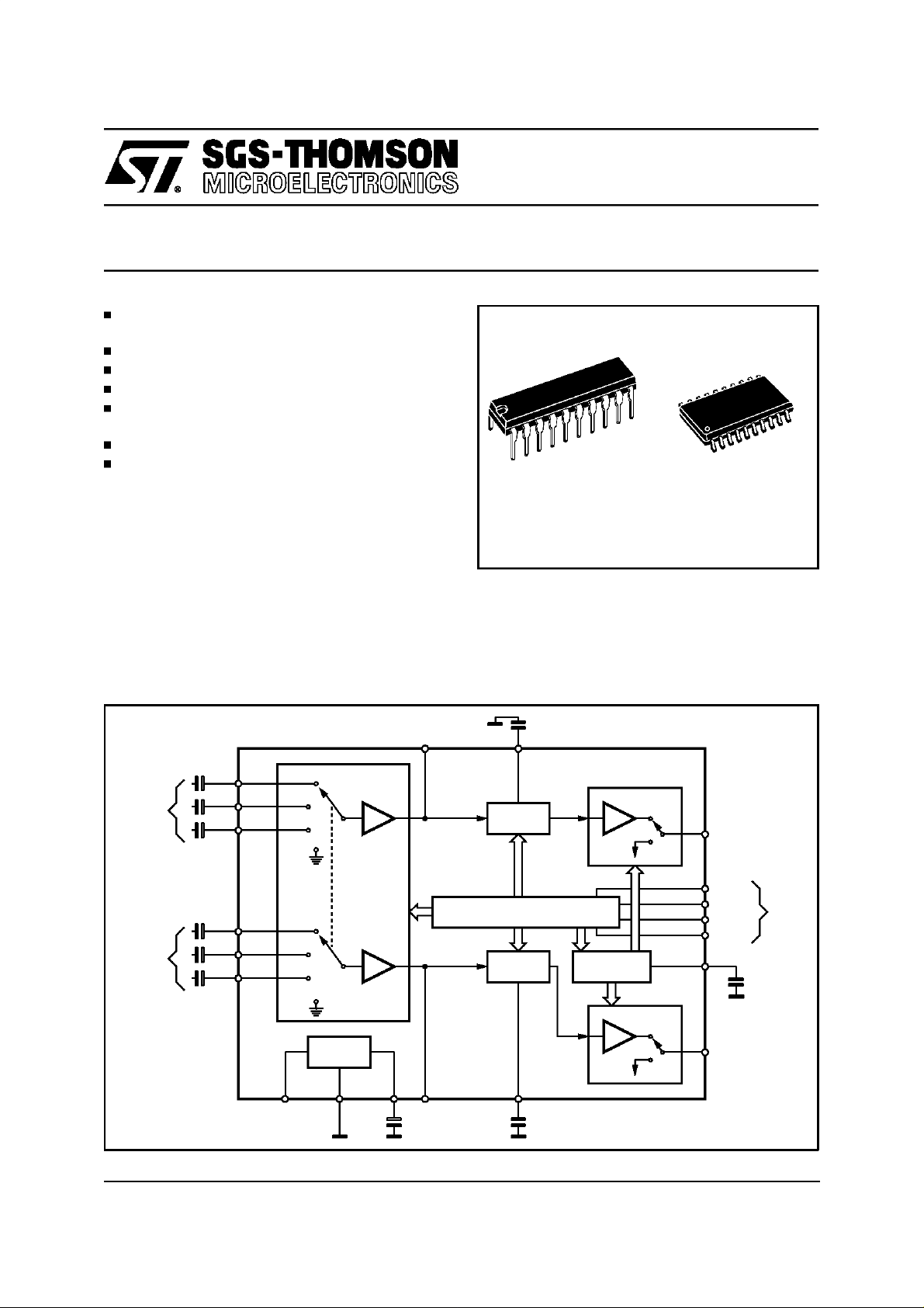
BLOCK DIAGRAM
x
3
2.2µF
LEFT
INPUTS
x
3
2.2µF
RIGHT
INPUTS
17
18
20
14
13
11
INPUT
SELECTOR
SUPPLY
16 7 15
AGNDV
S
CREF
Recout(L)
1
TDA7309
10
Recout(R)
22µF
LOUD(L)
VOLUME
LOUDNESS
VOLUME
LOUDNESS
LOUD(R)
100nF
19
+
+
12
100nF
SOFT
MUTE
MUTE
MUTE
2
6
4
5
8
3 CSM
9
D93AU045A
OUT
LEFT
DIGGND
SDA
SCL
ADDR
OUT
RIGHT
BUSSERIAL BUS DECODER+ LATCHES
September 1997
1/12

TDA7309
PIN CONNECTION
(Top View)
RecoutL
OUTL
CSM
SDA
SCL
DGND
GND
ADD
OUTR
1
2
3
4
5
6
7
8
9 LOUDR
19
18
17
16
15
14
13
12
IN3L20
LOUDL
IN2L
IN1L
V
S
CREF
IN1R
IN2R
RecoutR 10 IN3R11
D94AU058A
ABSOLUTE MAXIMUM RATINGS
Symbol Parameter Value Unit
V
S
T
amb
T
stg
Operating Supply Voltage 10.5 V
Operating Ambient Temperature –40 to85 °C
Storage Temperature Range –55 to +150 °C
QUICK REFERENCE DATA
Symbol Parameter Test Condition Min. Typ. Max. Unit
V
S
V
CL
Operating Supply Voltage 6 10 V
Max. Input SignalHandling 2 Vrms
THD Total Harmonic Distortion V = 1Vrms, f= 1KHz 0.01 0.1 %
S/N Signal to Noise Ratio 106 dB
Sc Channel Separation f = 1KHz 100 dB
Volume Control 1.0dB step –95 0 dB
Soft Mute Attenuation 60 dB
Direct Mute Attenuation 100 dB
TEST CIRCUIT
IN1L
IN2L
IN3L
RecoutL
IN1R
IN2R
IN3R
RecoutR
17
18
20
1
TDA7309
14
13
101119 12 5 4 6
LL LR
SCL SDA DIGGND
CSM
3
2
OUTL
16
V
S
15 CREF
AGND7
OUTR9
8
ADD
2/12
D94AU057A

THERMAL DATA
Symbol Parameter SO20 DIP20 Unit
R
th j-pins
Thermal resistanceJunction to Pins 150 100
TDA7309
C/W
°
ELECTRICALCHARACTERISTICS (Refer to the test circuit, T
=50Ω, all controls flat (G = 0), f = 1KHzunless otherwisespecified.)
R
G
=25°C, VS= 9V, RL= 10KΩ,
amb
Symbol Parameter Test Condition Min. Typ. Max. Unit
SUPPLY
V
S
I
S
SVR Ripple Rejection 60 85 dB
Supply Voltage 5 (*) 9 10 V
Supply Current 7 10 mA
INPUT SELECTORS
R
S
in
Input Resistance 35 50 65 KΩ
I
Input Separation 80 90 dB
VOLUMECONTROL
C
RANGE
A
VMAX
A
STEP
E
A
E
T
V
DC
A
mute
Control Range 92 dB
Max. Attenuation 87 92 95 dB
Step resolution 0.5 1 1.5 dB
Attenuation Set Error AV= 0to -24dB -1.2 1.2 dB
A
= -24to -56dB -3 2 dB
V
Tracking Error 2dB
DC Steps adjacent attenuationsteps 0 3 mV
from 0dB to A
max. 0.5 5 mV
V
Output Mute Attenuation 80 100 dB
SOFT MUTE
T
d
Delay Time C
= 22nF 0 to –20dB
smute
Fast Mode
Slow Mode
1
20
AUDIO OUTPUTS
ms
ms
V
R
R
V
CLIP
L
out
DC
Clipping Level d = 0.3% 2 2.6 Vrms
Output Load Resistance 2 KΩ
Output Impedance 100 200 300 Ω
DC Voltage Level 3.8 V
GENERAL
e
NO
Et Total Tracking Error A
S/N Signal to Noise Ratio all gains = 0dB; V
d Distortion 0.01 0.1 %
S
C
Output Noise BW = 20-20KHz, flat
output muted
all gains = 0dB
2.5
515
A curve allgains = 0dB 3 µV
= 0to –24dB
V
A
= -24to –56dB
V
= 1Vrms 95 106 dB
O
0
0
Channel Separation 80 100 dB
BUS INPUTS
V
IL
V
IH
I
IN
V
O
(*) Hedevice work until 5V but noguarantee about SVR
Input Low Voltage 1V
Input High Voltage 3 V
Input Current Vin= 0.4V -5 +5
Output Voltage SDA
IO= 1.6mA 0.4 0.8 V
Acknowledge
µV
V
µ
1
2
dB
dB
µ
A
3/12
TDA7309
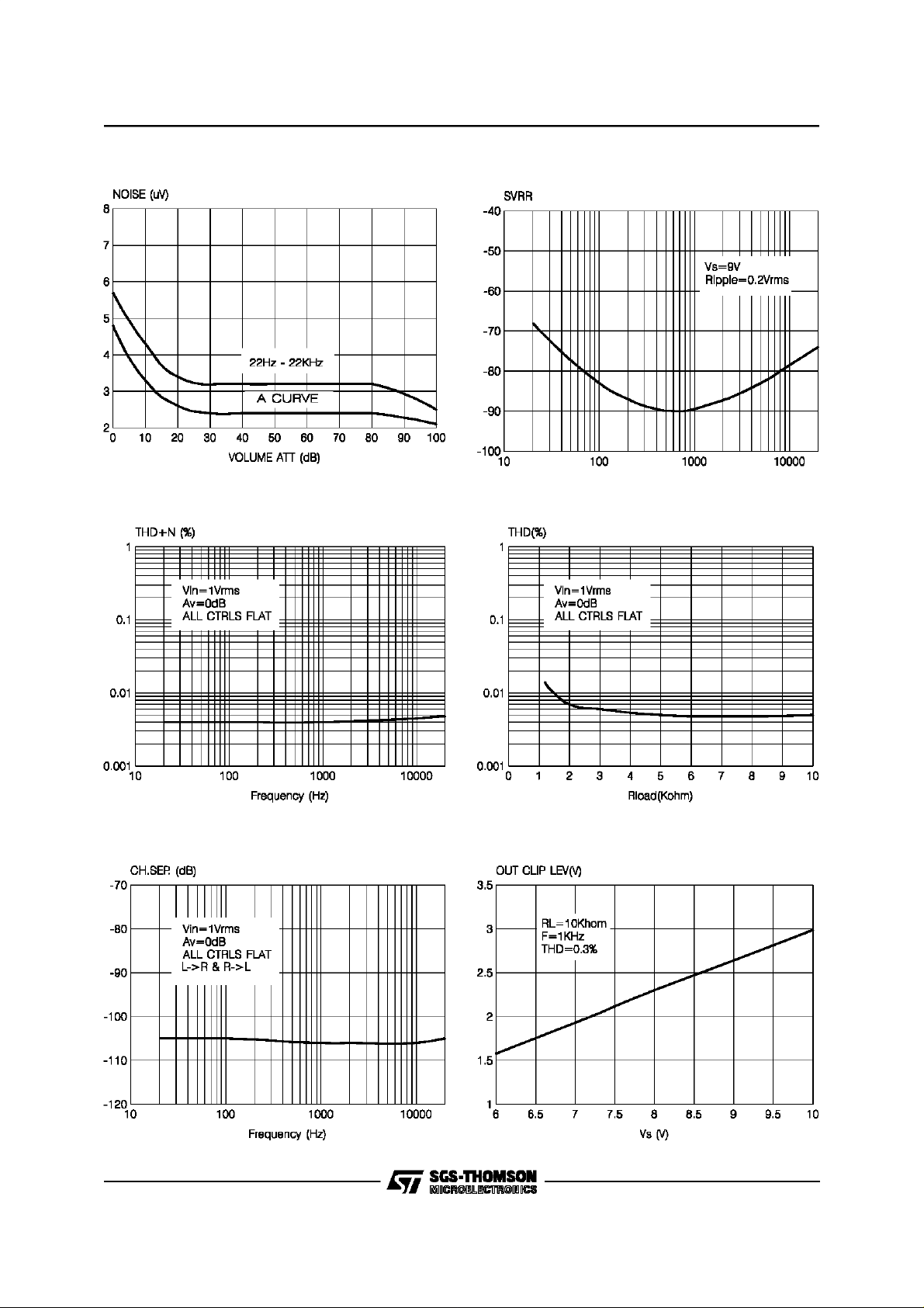
Figure 1:
Noisevs. volumesetting.
Figure 3: THD vs. frequency
Figure2: SVRR vs. frequency.
Figure4: THD vs. R
LOAD
.
Figure 5:
4/12
Channelseparationvs. frequency.
Figure6:
Outputclip level vs.Supply Voltage.

TDA7309
Figure 7:
Quiescentcurrent vs.supply voltage.
Figure 9: Loudnesvs. Frequency
(C
= 100nF)vs. Volume
LOUD
Figure8: Loudnessvs. VolumeAttenuation.
Figure10:
Loudnessvs. External Capacitors
5/12

TDA7309
I2C BUSINTERFACE
Data transmission from microprocessor to the
TDA7313 and viceversa takes place thru the 2
wires I
2
C BUS interface, consisting of the two
lines SDA and SCL (pull-up resistors to positive
supply voltage must be connected).
Data Validity
As shown in fig. 11, the data on the SDA line
must be stable during the high period of theclock.
The HIGH and LOW state of the data line can
only change when the clock signal on the SCL
line is LOW.
Start and Stop Conditions
As shown in fig. 12 a start condition is a HIGH to
LOW transition of the SDA line while SCL is
HIGH. The stop condition is a LOW to HIGH transition of the SDA line while SCL is HIGH.
Byte Format
Every byte transferred on the SDA line must contain 8 bits. Each byte must be followed by an acknowledgebit. The MSB istransferredfirst.
Figure11:
DataValidity on the I
2
CBUS
Acknowledge
The master(µP) puts a resistive HIGH level on the
SDA line during the acknowledgeclock pulse (see
fig. 13). The peripheral (audioprocessor) that acknowledges has to pull-down (LOW) the SDA line
during the acknowledge clock pulse, so that the
SDAlineis stableLOWduringthisclockpulse.
The audioprocessor which has been addressed
has to generate an acknowledge after the reception of each byte, otherwise the SDAline remains
at the HIGH level during the ninth clock pulse
time. In this case the master transmitter can generate the STOP information in order to abort the
transfer.
Transmissionwithout Acknowledge
Avoiding to detect the acknowledge of the audioprocessor, the µP can use a simplier transmission: simply it waits one clock without checking
the slave acknowledging, and sends the new
data.
This approach of course is less protected from
misworkingand decreasesthe noiseimmunity.
Figure 12:
Figure 13:
6/12
TimingDiagramof I
2
Acknowledgeon the I
CBUS
2
CBUS

TDA7309
SDA, SCLI2CBUSTIMING
Symbol Parameter Min. Typ. Max. Unit
f
SCL
t
BUF
t
HD:STA
t
LOW
t
HIGH
t
SU:STA
t
HD:DA
t
SU:DAT
t
R
t
F
t
SU:STO
All values referred to V
(*) Must be guaranteed by the I
SCL clock frequency 0 400 kHz
Bus free timebetween a STOP and START condition 1.3 µs
Hold time (repeated)START condition. After this period,the first
0.6
clock pulse is generated
LOW period of the SCL clock 1.3 µs
HIGH period of the SCL clock 0.6 µs
Set-up time for a repeated START condition 0.6 µs
Data hold time 0.300 µs
Data set-up time 100 ns
Rise time ofboth SDA and SCL signals 20 300 ns (*)
Fall time of both SDA and SCL signals 20 300 ns (*)
Set-up time for STOP condition 0.6 µs
IH min.
and V
levels
IL max.
2
C BUS master.
s
µ
Definitionof timingon the I2C-bus
SDA
t
SCL
PS
P=
S = START
BUF
STOP
t
HD;STA
t
LOW
t
RtF
t
HD;DAT
t
HIGH
t
t
HD;STA
t
t
SU;DAT
SU;STA
Sr P
D95AU314
t
F
SU;STO
t
SP
7/12

TDA7309
SOFTWARESPECIFICATION
Interface Protocol
The interface protocol comprises:
A start condition (s)
A chip address byte, containing the TDA7309
TDA7309 ADDRESS
MSB
S001100A0
ACK = Acknowledge
S = Start
P = Stop
MAX CLOCK SPEED 100kbits/s
first byte
LSB MSB LSB MSB LSB
ACK DATA ACK DATA ACK P
SOFTWARESPECIFICATION
Chip address
address(the 8th bit of the byte must be 0). The
TDA7309must always acknowledgeat the end
of each transmittedbyte.
A sequenceof data (N-bytes + acknowledge)
A stopcondition (P)
Data Transferred (N-bytes + Acknowledge)
MSB LSB
00110010pin address open
00110000pin address close to ground
FUNCTIONCODES
MSB F6 F5 F4 F3 F2 F1 LSB
VOLUME 0XXXXXXX
MUTE/LOUD 100XXXXX
INPUTS 101XXXXX
CHANNEL 110XXXXX
CHANNEL ABILITATIONCODES
MSB F6 F5 F4 F3 F2 F1 LSB FUNCTION
1 1 0 channel
X X X 0 0 RIGHT
X X X 0 1 LEFT
X X X 1 0 BOTH
X X X 1 1 BOTH
Power on reset condition
11111110
8/12

VOLUMECODES
MSB F6 F5 F4 F3 F2 F1 LSB FUNCTION
0 step 1dB
0 0 0 0dB
0 0 1 -1dB
0 1 0 -2dB
0 1 1 -3dB
1 0 0 -4dB
1 0 1 -5dB
1 1 0 -6dB
1 1 1 -7dB
0 step 8dB
0000 0dB
0 0 0 1 -8dB
0 0 1 0 -16dB
0 0 1 1 -24dB
0 1 0 0 -32dB
0 1 0 1 -40dB
0 1 1 0 -48dB
0 1 1 1 -56dB
1 0 0 0 -64dB
1 0 0 1 -72dB
1 0 1 0 -80dB
1 0 1 1 -88dB
1 1 X X MUTE
MUTE LOUDNESS CODES
TDA7309
MSB F6 F5 F4 F3 F2 F1 LSB FUNCTION
1 0 0 mute/loud
X 0 0 slow soft mute on
X 0 1 fast soft mute on
1 soft mute off
1 LOUD OFF
X 0 0 loud on (10dB)
X 1 0 loud on (20dB)
INPUT MULTIPLEXERCODES
MSB F6 F5 F4 F3 F2 F1 LSB FUNCTION
101 inputs
XXX00 MUTE
X X X 0 1 IN2
X X X 1 0 IN3
X X X 1 1 IN1
Purchaseof I
2
I
C Patent Rights to use these components in an I2C system, provided that the system conforms to
2
C StandardSpecificationsas defined by Philips.
the I
2
C Componentsof SGS-THOMSON Microlectronics, conveys a license underthe Philips
9/12

TDA7309
SO20 PACKAGEMECHANICAL DATA
DIM.
MIN. TYP. MAX. MIN. TYP. MAX.
A 2.65 0.104
a1 0.1 0.3 0.004 0.012
a2 2.45 0.096
b 0.35 0.49 0.014 0.019
b1 0.23 0.32 0.009 0.013
C 0.5 0.020
c1 45 (typ.)
D 12.6 13.0 0.496 0.512
E 10 10.65 0.394 0.419
e 1.27 0.050
e3 11.43 0.450
F 7.4 7.6 0.291 0.299
L 0.5 1.27 0.020 0.050
M 0.75 0.030
S 8 (max.)
mm inch
10/12

DIP20 PACKAGE MECHANICAL DATA
TDA7309
DIM.
MIN. TYP. MAX. MIN. TYP. MAX.
a1 0.254 0.010
B 1.39 1.65 0.055 0.065
b 0.45 0.018
b1 0.25 0.010
D 25.4 1.000
E 8.5 0.335
e 2.54 0.100
e3 22.86 0.900
F 7.1 0.280
I 3.93 0.155
L 3.3 0.130
Z 1.34 0.053
mm inch
11/12

TDA7309
Information furnished is believed to be accurate and reliable. However, SGS-THOMSON Microelectronics assumes no responsibility for the
consequences of use of such information nor for any infringement of patents or other rights of third parties which may result from its use.No
license is granted by implication or otherwise under any patent or patent rights of SGS-THOMSON Microelectronics. Specification mentioned
in this publication are subject to change without notice. This publication supersedes and replaces all information previously supplied. SGSTHOMSON Microelectronics products are not authorized for use as critical components in life support devices or systems without express
written approval of SGS-THOMSON Microelectronics.
1997 SGS-THOMSON Microelectronics – Printed in Italy – All Rights Reserved
SGS-THOMSON Microelectronics GROUP OF COMPANIES
Australia - Brazil - Canada - China - France - Germany - HongKong - Italy - Japan - Korea - Malaysia - Malta - Morocco - The Netherlands -
Singapore - Spain - Sweden - Switzerland - Taiwan - Thailand - United Kingdom - U.S.A.
12/12
 Loading...