

DIGITAL CONTROLLED STEREO AUDIO PROCESSOR
SINGLESUPPLYOPERATION
FOUR STEREO INPUT SOURCE SELEC-
TION
MONOINPUT
TREBLE, BASS, VOLUME, AND BALANCE
CONTROL
FOUR INDEPENDENT SPEAKER CONTROL
(FRONT/REAR)
SINGLESUPPLYOPERATION
ALL FUNCTIONS PROGRAMMABLE VIA SE-
RIALBUS
VERY LOW NOISE AND VERY LOW DIS-
TORTION
POP FREE SWITCHING
DESCRIPTION
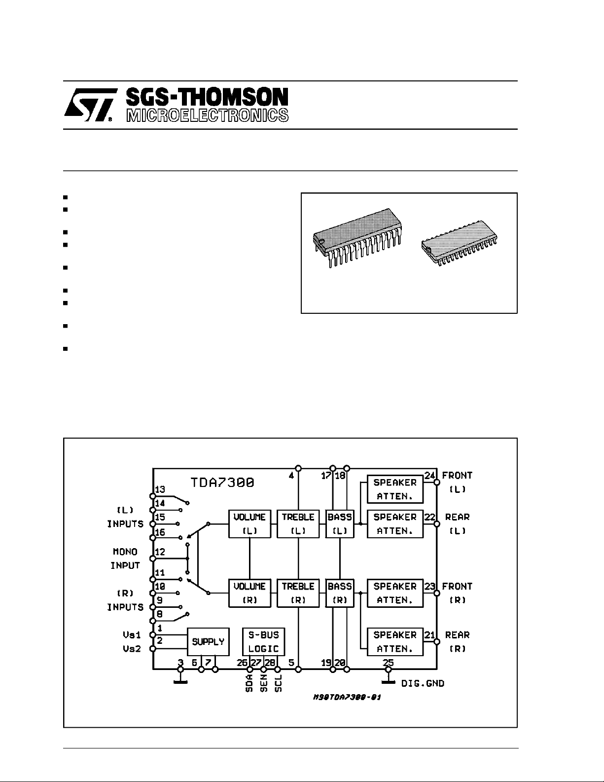
The TDA7300 is a volume, tone (bass and treble),
balance (left/right) and fader (front/rear) proces-
TDA7300
DIP28 SO28
ORDERING NUMBERS:
TDA7300 TDA7300D
sor for high quality audio applicationsin car radio
and Hi-Fi systems.
Control is accomplished by serial bus microprocessorinterface.
The AC signal setting is obtained by resistor networksand analog switches combined with operational amplifiers.
The results are: low noise, low distortion andhigh
dynamicrange.
BLOCK DIAGRAM
May 1991
This isadvanced information on anew product now in development or undergoing evaluation. Details are subject tochange withoutnotice.
1/16
TDA7300
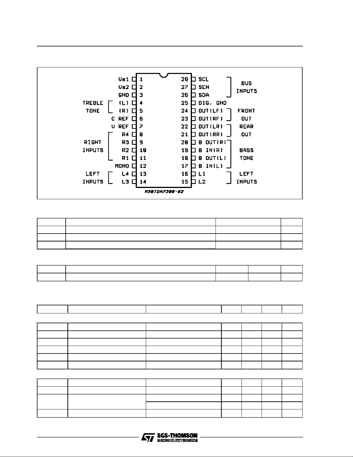
PIN CONNECTION (Top view)
ABSOLUTE MAXIMUM RATINGS
Symbol Parameter Value Unit
V
T
amb
T
Supply Voltage (VS1)18V
S
Operating Ambient Temperature Range -40 to +85 °C
Storage Temperature -40 to 150 °C
stg
THERMAL DATA
Symbol Description SO28 DIP28 Unit
R
th j-pins
ELECTRICALCHARACTERISTICS (T
Thermal Resistance Junction-pins Max 85 65 °C/W
=25°C,VS1= 12V or VS2= 8.5V , RL= 10kΩ andRg=600Ω ,
amb
f = 1KHz unlessotherwisespecified)
Symbol Parameter Test Condition Min. Typ. Max. Unit
SUPPLY(1)
V
S1
V
S2
I
S2
V
ref
SVR Ripple Rejection at V
SVR Ripple Rejection at V
Supply VoltageVS1 10 12 16 V
Supply VoltageVS2 6 8.5 10 V
Supply Current 15 30 40 mA
Reference Voltage (pin 7) 3.5 4.3 5 V
S1
S2
f = 300Hz to 10KHz 80 97 dB
f = 300Hz to 10KHz 50 58 dB
INPUTSELECTORS
V
V
R
IN max
IN
i (DC)
Input Resistance 30 45 KΩ
i
Max. Input Signal GV = 0dB d =0.3% 1.5 2.2 Vrms
Input Separation f = 1KHz (2) 90 100 dB
S
f = 10KHz (2) 70 80 dB
Input DC Voltage 3.5 4.3 5 V
2/16
TDA7300
ELECTRICALCHARACTERISTICS (continued)
Symbol Parameter Test Condition Min. Typ. Max. Unit
VOLUMECONTROLS
Control Range 78 dB
G
max
SPEAKERATTENUATORS
BASSAND TREBLE CONTROL (3)
AUDIOOUTPUT
V
O
R
L
C
L
R
O
(DC) DC Voltage Level 3 3.8 4.5 V
V
O
GENERAL
e
NO
S/N Signal to Noise Ratio All gain= 0dB V
d Distortion f = 1KHz; V
S
C
BUS INPUTS
V
IL
V
IH
V
O
Notes:
(1) The circuit can be supplied either at V
voltage V
of about 0.8V.
(2) The selected input is grounded thru the 2.2µF capacitor.
(3) Bass and Trebleresponse see attacheddiagram. The center frequencyand quality of the resonance behaviour can be choosenby the
external circuitry. A standard firstorder bassresponse can berealized by a standard feedback network.
Max Gain 8 10 12 dB
Max Attenuation 64 68 dB
Step Resolution G
= -50 to 10dB 2 3 dB
V
Attenuator Set Error 2 dB
Tracking Error 2dB
Control Range 35 38 41 dB
Step Resolution 2 3 dB
Attenuator Set Error 2 dB
Tracking Error 2dB
Control Range ±15 dB
Step Resolution 2.5 3.5 dB
Max. Output Voltage d = 0.3% 1.5 2.2 Vrms
Output Load Resistance 2 KΩ
Output Load Capacitance 1 nF
Output Resistance 70 150 Ω
Output Noise BW = 22Hz to 22KHz, Gv= 0dB 6 15
Curve A Gv= 0dB 4
= 1Vrms
O
105 dB
BW = 22Hz to 22KHz
= 1V; Gv= 0 0.01 0.1 %
O
Frequency Response (-1dB) G
= 0 High
v
Channnel Separation left/right f = 1KHz
f = 10KHz
Low
20
90
70
20
KHz
100
80
Input LOW Voltage 0.8 V
Input HIGH Voltage 2.4 V
OutputVoltageSDAAcknowledge I = 1.6mA 0.4 V
Digital Input Current -5 +5 µA
or without the use of the internal voltage regulator at VS2. The circuit also operates at a supply
lower than 10V. In this case the ripple rejection of VS2is valid, because the voltage regulator saturates to asaturation voltage
S1
S1
µV
Hz
dB
dB
3/16
TDA7300
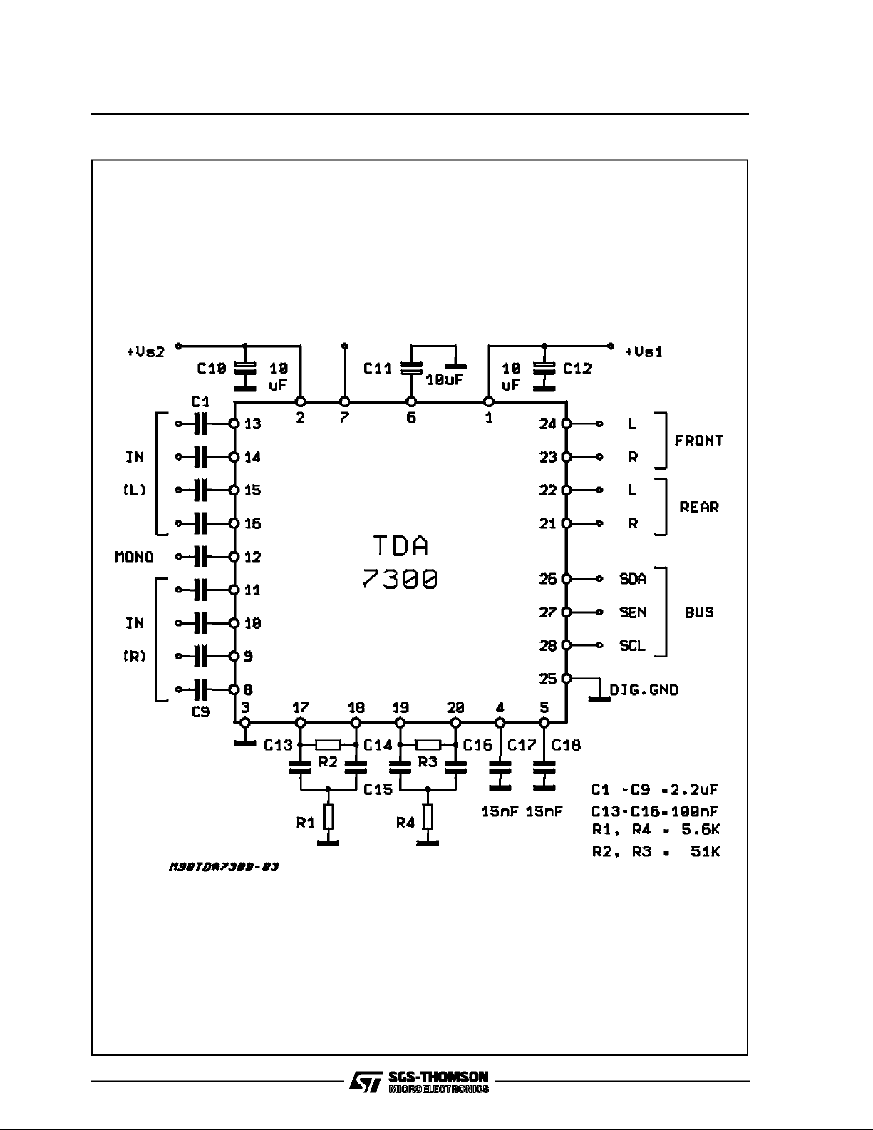
Figure1: ApplicationCircuit
4/16
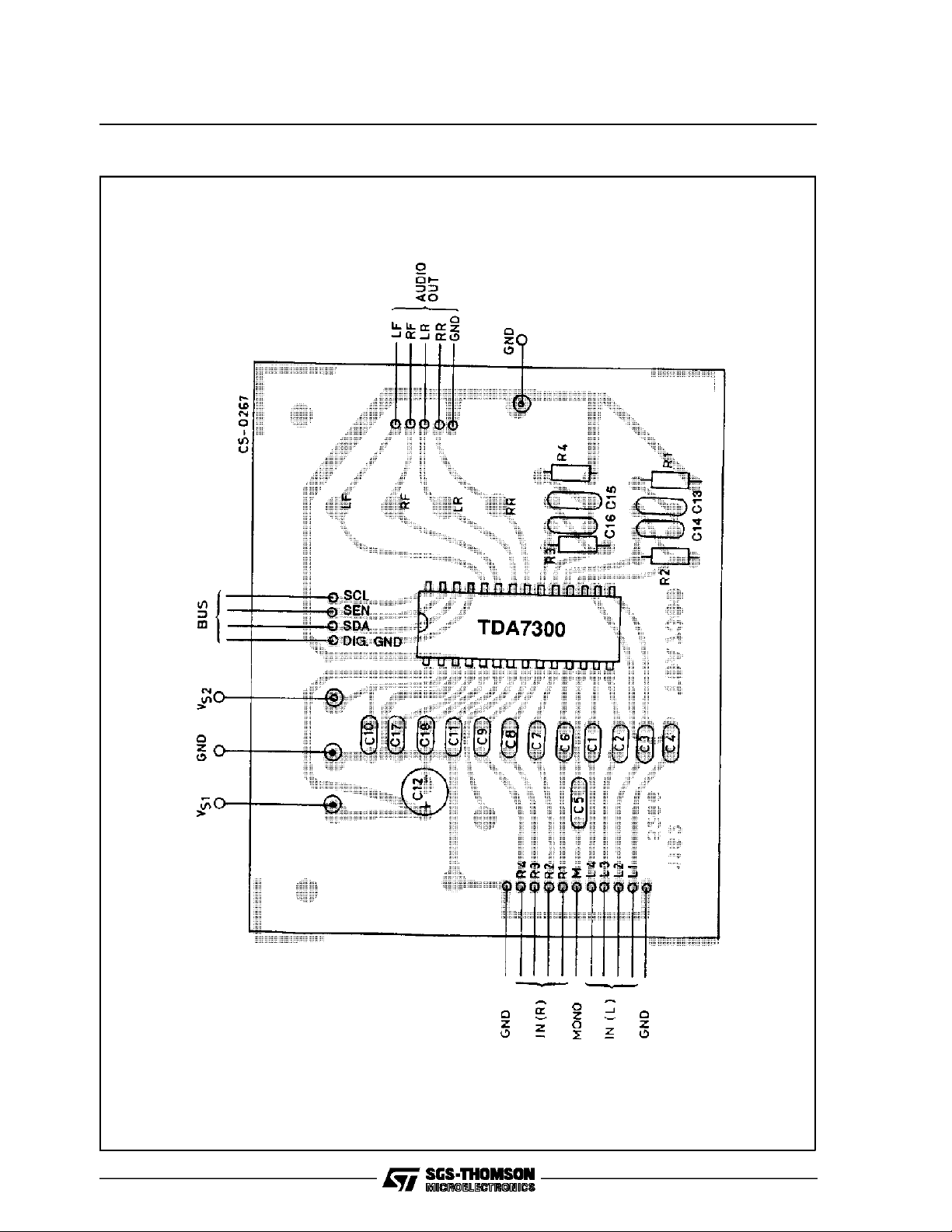
Figure2: P.C. Board and ComponentsLayout of theFig.1 (1:1scale)
TDA7300
5/16
TDA7300
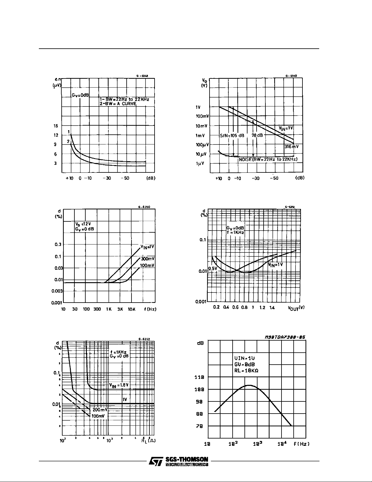
Figure3: Total Output Noisevs. VolumeSetting
Figure5: Distortion+ Noise vs. Frequency
Figure4: Signalto NoiseRatio vs. Volume
Setting
Figure6: Distortionvs. OutputVoltage
Figure7: Distortionvs. LoadResistance
6/16
Figure8: ChannelSeparation(L1 -R1) vs.
Frequency

TDA7300
Figure9: Input Separation(L1 - L2) vs. (VS1)
Frequency
Figure11: SupplyVoltageRejection (V
S2
)vs.
Frequency
Figure10: Supply VoltageRejection(V
S1
Frequency
Figure12: SupplyVoltageRejection vs. V
)vs.
S1
Figure13: SupplyVoltageRejection vs. V
S2
Figure14: Clipping Level(Vrms) vs. Supply
Voltage
7/16

TDA7300
APPLICATIONINFORMATION
Volume Control Concept
Traditionalelectronic volume control circuitsuse a
multiplier technique with all the disadvantages of
high noise anddistortion.
The used concept, as shown in Fig. 15 with digital
switchedresistor dividers, providesextremely low
noise anddistortion. The multiplexing of the resistive dividers is realized with a multiple-input operationalamplifier.
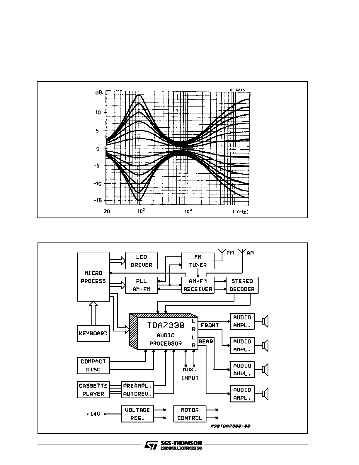
Bass and TrebleControl
The principle operation of the bass control is
shown in Fig. 16. The external filter together with
the internalbufferallows a flexible filterdesign according to the differentrequirementsin car radios.
The functionof the treble issimilar to thebass.
A typicalcurve is shown in Fig.19.
Outputs
A special class-A output amplifier with a modulated sink current provides low distortion and
ground compatibility with low current consumption.
Figure16: BassControl
Figure17: QuiescentCurrent vs. SupplyVoltage
Figure15: VolumeControl
Figure18: QuiescentCurrent vs. Temperature
8/16
APPLICATION INFORMATION (continued)
Figure 19: TypicalTone Response
TDA7300
Figure20: CompleteCar-RadioSystemusing DigitalControlledAudioProcessor
9/16

TDA7300
APPLICATIONINFORMATION (continued)
SERIALBUS INTERFACE
S-BUS Interfaceand I
2
CBUSCompatibility
Data transmission from microprocessor to the
TDA7300 and viceversa takes place thru the 3wire S-BUS interface, consisting of the three lines
SDA, SCL, SEN. If SDA and SEN inputs are
short-circuited together, then the TDA7300 appearsas a standardI
According to I
2
CBUS slave.
2
CBUS specification the S-BUS
lines are connected to a positive supply voltage
via pull-up resistors.
DataValidity
As shown in fig. 21, the data on the SDA line
mustbe stable during the highperiod of the clock.
The HIGH and LOW state of the data line can
only change when the clock signal on the SCL
line is LOW.
2
Figure21: Data Validity on the I
CBUS
Startand StopConditions
2
I
CBUS:
as shown in fig.22 a start condition is a HIGH to
2
Figure22: TimingDiagram of S-BUSand I
CBUS
LOW transition of the SDA line while SCL is
HIGH. The stop condition is a LOWto HIGH transitionof the SDA line while SCL is HIGH.
S-bus:
the start/stop conditions (points 1 and 6) are detected exclusively by a transition of the SEN line
(1 → 0/0→1)while the SCLline is at the HIGH
level.
TheSDA line is only allowed to change during the
time the SCL line is low (points 2, 3, 4, 5). After
the start information(point 1) the SEN line returns
to the HIGH level and remains unchanged for all
the timethe transmission is performed.
Byte Format
Every byte transferred on the SDA line must contain 8 bits. Each byte must be followed by an acknowledgebit. TheMSBis transferredfirst.
Acknowledge
The master (µP) puts a resistive HIGH level on the
SDA line during the acknowledgeclock pulse (see
fig. 23). The peripheral (audioprocessor) that acknowledgeshas to pull-down (LOW) the SDA line
during the acknowledge clock pulse, so that the
SDAline is stableLOW duringthisclockpulse.
The audioprocessor which has been addressed
has to generate an acknowledge after the receptionof each byte, otherwisethe SDA line remains
at the HIGH level during the ninth clock pulse
time. In this case the master transmitter can generate the STOP information in order to abort the
transfer.
10/16

TDA7300
APPLICATIONINFORMATION (continued)
Figure23: Acknowledgeon the I
2
CBUS
TransmissionwithoutAcknowledge
Avoiding to detect the acknowledge of the audioprocessor,the µP can use a simplier transmission:
simplyit waitsone clockwithoutcheckingthe slave
acknowledging,and sendsthenewdata.
This approach of course is less protected from
misworking and decreasesthe noiseimmunity.
TDA7300 ADDRESS
InterfaceProtocol
Theinterface protocol comprises:
A start condition (S)
A chip address byte, containing the TDA7300
address(the 8th bitof the byte must be 0).The
TDA7300mustalways acknowledge at theend
ofeach transmittedbyte.
A sequence of data (N-bytes+ acknowledge)
A stop condition(P)
MSB first byte LSB MSB LSB MSB LSB
S10001000
ACK = Acknowledge
S = Start
P = Stop
MAX CLOCK SPEED100kbits/s
DATABYTES
MSB LSB
A1
A2
B0
B1
B2
0
0
1
1
1
1
0
1
0
1
1
0
1
0
1
0
X = don’t care
Ax = 2dB steps
Bx =10dB steps
Cx = 2.5dB steps
B1
0
B1
1
B1
0
B1
1
X
0
0
1
1
1
B0
B0
B0
B0
X
C3
C3
A2
A2
A2
A2
S2
C2
C2
A1
A1
A1
A1
S1
C1
C1
ACK DATA ACK DATA AC K P
Data Transferred (N-bytes + Acknowledge)
SOFTWARE SPECIFICATION
Chip address(TDA7300address)
10001000
MSB IIIIILSB
Statusafter power-on reset
Function
Volume Control
A0
Speaker ATT LR
A0
Speaker ATT RR
A0
Speaker ATT LF
A0
Speaker ATT RF
A0
Audio switch
S0
Bass control
C0
Treble control
C0
Volume
Speaker
Audio Switch
Bass
Treble
–68dB
–38dB
Mono
+2.5dB
+2.5dB
11/16

TDA7300
SOFTWARE SPECIFICATION (continued)
DATABYTES (detaileddescription)
VOLUME
MSB LSB
0 0 B2 B1 B0 A2 A1 A0 Volume 2dB Steps
0
0
0
0
0
0
1
0
1
0
0
1
0
1
1
1
1
1
0 0 B2 B1 B0 Volume 10dB steps
0
0
0
0
0
0
1
1
1
1
1
0
0
1
1
1
0
0
1
0
0
1
1
1
1
0
1
0
1
0
1
-2
-4
-6
-8
Not allowed
Not allowed
Not allowed
+10
0
-10
-20
-30
-40
-50
-60
For example if you want setting the volumeat -32dBthe 8 bit stringis: 0 0 1 0 0 00 1
SPEAKERATTENUATORS
MSB LSB
Speaker LF
A0
A1
A2
B0
B1
0
0
1
1
1
1
1
0
0
1
1
1
B1
B1
B1
B0
B0
B0
0
0
1
0
0
1
1
1
A2
A2
A2
A1
A1
A1
0
0
0
0
1
0
1
0
0
1
0
1
1
1
1
1
A0
A0
A0
0
1
0
1
0
1
0
1
Speaker RF
Speaker LR
Speaker RR
0
-2
-4
-6
-8
Not allowed
Not allowed
Not allowed
0
-10
-20
-30
For example attenuationof 24dBon speakerRF is given by: 1 0 1 10010
12/16

SOFTWARE SPECIFICATION (continued)
AUDIOSWITCH - Select the inputChannel to Activate
MSB LSB
0 1 0 X X S2 S1 S0 Audio Switch
Stereo 1
0
0
0
X
X
X
X
X
X
X
X
X
X
X
X
X
X
X
X
0
0
1
0
1
0
0
1
0
1
1
1
1
1
1
0
1
0
1
0
1
Stereo 2
Stereo 3
Stereo 4
Mono
Not Allowed
Not Allowed
Not Allowed
X =don’t care
For example to set the stereo 2 channelthe 8 bit stringmay be: 01 0 00 0 0 1
BASSAND TREBLE - ControlRangeof ± 15dB (boost and cut) Stepsof 2.5dB
0
1
0
1
1
1
0
C3C3C2C2C1C1C0
1
0
0
0
0
0
0
0
0
0
0
0
0
1
1
1
1
C0
0
0
1
1
0
0
1
1
0
1
0
1
0
1
0
1
Treble
TDA7300
Bass
-15
-15
- 12.5
-10
- 7.5
-5
- 2.5
-0
1
1
1
1
1
1
1
1
1
1
1
1
0
0
0
0
1
1
0
0
1
1
0
0
1
0
1
0
1
0
1
0
0
2.5
5
7.5
10
12.5
15
15
C3 =Sign
For example Bass at -12.5dBis obtained by thefollowing8 bit string: 0 1 1 0 0 0 10
13/16

TDA7300
DIP28 PACKAGEMECHANICAL DATA
DIM.
MIN. TYP. MAX. MIN. TYP. MAX.
a1 0.63 0.025
b 0.45 0.018
b1 0.23 0.31 0.009 0.012
b2 1.27 0.050
D 37.34 1.470
E 15.2 16.68 0.598 0.657
e 2.54 0.100
e3 33.02 1.300
F 14.1 0.555
I 4.445 0.175
L 3.3 0.130
mm inch
14/16

SO28PACKAGE MECHANICAL DATA
TDA7300
DIM.
MIN. TYP. MAX. MIN. TYP. MAX.
A 2.65 0.104
a1 0.1 0.3 0.004 0.012
b 0.35 0.49 0.014 0.019
b1 0.23 0.32 0.009 0.013
C 0.5 0.020
c1 45° (typ.)
D 17.7 18.1 0.697 0.713
E 10 10.65 0.394 0.419
e 1.27 0.050
e3 16.51 0.65
F 7.4 7.6 0.291 0.299
L 0.4 1.27 0.016 0.050
S8°(max.)
mm inch
15/16

TDA7300
Information furnished is believed to be accurate and reliable. However, SGS-THOMSON Microelectronics assumes no responsibility for the
consequences of use of such informationnor forany infringement ofpatents or otherrights of third partieswhich may resultfrom itsuse. No
license is granted by implication or otherwise under any patent or patent rights of SGS-THOMSON Microelectronics. Specifications mentioned in this publication are subject to change without notice. This publication supersedesand replaces all informationpreviously supplied.
SGS-THOMSON Microelectronics products are not authorized for use as critical components in life support devices or systems without express written approval of SGS-THOMSONMicroelectronics.
2
Purchase of I
Australia - Brazil- France -Germany - Hong Kong-Italy - Japan - Korea -Malaysia - Malta - Morocco - The Netherlands- Singapore -
C Components ofSGS-THOMSONMicroelectronics, conveys a licenseunder the PhilipsI2C PatentRights touse thesecompo-
nents in an I
2
C system, providedthat the systemconforms to the I2C Standard Specifications as defined by Philips.
1994 SGS-THOMSON Microelectronics - All RightsReserved
SGS-THOMSON Microelectronics GROUPOF COMPANIES
Spain - Sweden - Switzerland - Taiwan - Thaliand- United Kingdom - U.S.A.
16/16
 Loading...