

SGS Thomson Microelectronics TDA7300D, TDA7300 Datasheet
DIGITAL CONTROLLED STEREO AUDIO PROCESSOR
SINGLESUPPLYOPERATION
FOUR STEREO INPUT SOURCE SELEC-
TION
MONOINPUT
TREBLE, BASS, VOLUME, AND BALANCE
CONTROL
FOUR INDEPENDENT SPEAKER CONTROL
(FRONT/REAR)
SINGLESUPPLYOPERATION
ALL FUNCTIONS PROGRAMMABLE VIA SE-
RIALBUS
VERY LOW NOISE AND VERY LOW DIS-
TORTION
POP FREE SWITCHING
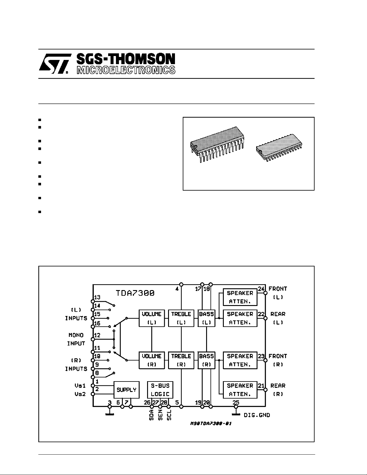
DESCRIPTION
The TDA7300 is a volume, tone (bass and treble),
balance (left/right) and fader (front/rear) proces-
TDA7300
DIP28 SO28
ORDERING NUMBERS:
TDA7300 TDA7300D
sor for high quality audio applicationsin car radio
and Hi-Fi systems.
Control is accomplished by serial bus microprocessorinterface.
The AC signal setting is obtained by resistor networksand analog switches combined with operational amplifiers.
The results are: low noise, low distortion andhigh
dynamicrange.
BLOCK DIAGRAM
May 1991
This isadvanced information on anew product now in development or undergoing evaluation. Details are subject tochange withoutnotice.
1/16
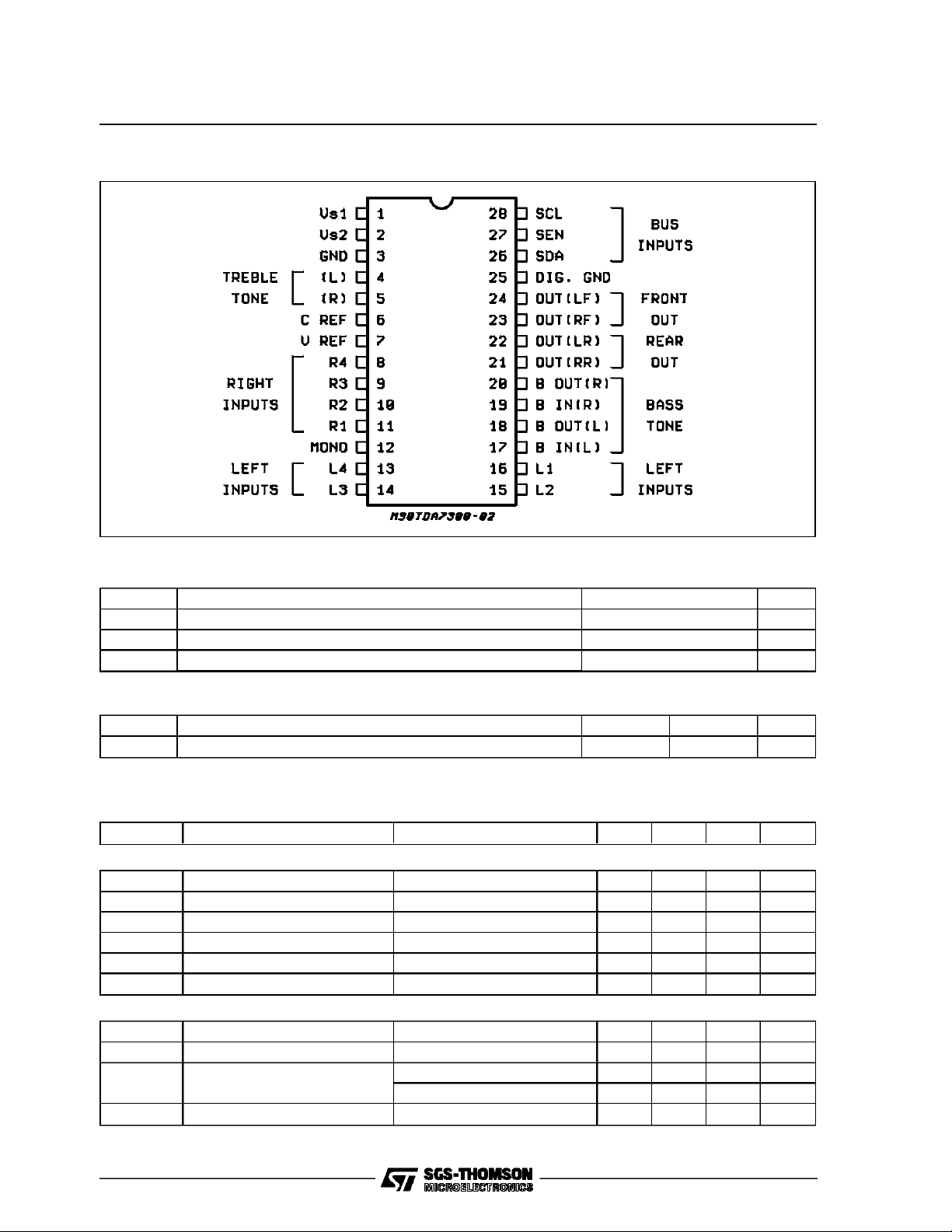
TDA7300
PIN CONNECTION (Top view)
ABSOLUTE MAXIMUM RATINGS
Symbol Parameter Value Unit
V
T
amb
T
Supply Voltage (VS1)18V
S
Operating Ambient Temperature Range -40 to +85 °C
Storage Temperature -40 to 150 °C
stg
THERMAL DATA
Symbol Description SO28 DIP28 Unit
R
th j-pins
ELECTRICALCHARACTERISTICS (T
Thermal Resistance Junction-pins Max 85 65 °C/W
=25°C,VS1= 12V or VS2= 8.5V , RL= 10kΩ andRg=600Ω ,
amb
f = 1KHz unlessotherwisespecified)
Symbol Parameter Test Condition Min. Typ. Max. Unit
SUPPLY(1)
V
S1
V
S2
I
S2
V
ref
SVR Ripple Rejection at V
SVR Ripple Rejection at V
Supply VoltageVS1 10 12 16 V
Supply VoltageVS2 6 8.5 10 V
Supply Current 15 30 40 mA
Reference Voltage (pin 7) 3.5 4.3 5 V
S1
S2
f = 300Hz to 10KHz 80 97 dB
f = 300Hz to 10KHz 50 58 dB
INPUTSELECTORS
V
V
R
IN max
IN
i (DC)
Input Resistance 30 45 KΩ
i
Max. Input Signal GV = 0dB d =0.3% 1.5 2.2 Vrms
Input Separation f = 1KHz (2) 90 100 dB
S
f = 10KHz (2) 70 80 dB
Input DC Voltage 3.5 4.3 5 V
2/16
TDA7300
ELECTRICALCHARACTERISTICS (continued)
Symbol Parameter Test Condition Min. Typ. Max. Unit
VOLUMECONTROLS
Control Range 78 dB
G
max
SPEAKERATTENUATORS
BASSAND TREBLE CONTROL (3)
AUDIOOUTPUT
V
O
R
L
C
L
R
O
(DC) DC Voltage Level 3 3.8 4.5 V
V
O
GENERAL
e
NO
S/N Signal to Noise Ratio All gain= 0dB V
d Distortion f = 1KHz; V
S
C
BUS INPUTS
V
IL
V
IH
V
O
Notes:
(1) The circuit can be supplied either at V
voltage V
of about 0.8V.
(2) The selected input is grounded thru the 2.2µF capacitor.
(3) Bass and Trebleresponse see attacheddiagram. The center frequencyand quality of the resonance behaviour can be choosenby the
external circuitry. A standard firstorder bassresponse can berealized by a standard feedback network.
Max Gain 8 10 12 dB
Max Attenuation 64 68 dB
Step Resolution G
= -50 to 10dB 2 3 dB
V
Attenuator Set Error 2 dB
Tracking Error 2dB
Control Range 35 38 41 dB
Step Resolution 2 3 dB
Attenuator Set Error 2 dB
Tracking Error 2dB
Control Range ±15 dB
Step Resolution 2.5 3.5 dB
Max. Output Voltage d = 0.3% 1.5 2.2 Vrms
Output Load Resistance 2 KΩ
Output Load Capacitance 1 nF
Output Resistance 70 150 Ω
Output Noise BW = 22Hz to 22KHz, Gv= 0dB 6 15
Curve A Gv= 0dB 4
= 1Vrms
O
105 dB
BW = 22Hz to 22KHz
= 1V; Gv= 0 0.01 0.1 %
O
Frequency Response (-1dB) G
= 0 High
v
Channnel Separation left/right f = 1KHz
f = 10KHz
Low
20
90
70
20
KHz
100
80
Input LOW Voltage 0.8 V
Input HIGH Voltage 2.4 V
OutputVoltageSDAAcknowledge I = 1.6mA 0.4 V
Digital Input Current -5 +5 µA
or without the use of the internal voltage regulator at VS2. The circuit also operates at a supply
lower than 10V. In this case the ripple rejection of VS2is valid, because the voltage regulator saturates to asaturation voltage
S1
S1
µV
Hz
dB
dB
3/16
TDA7300
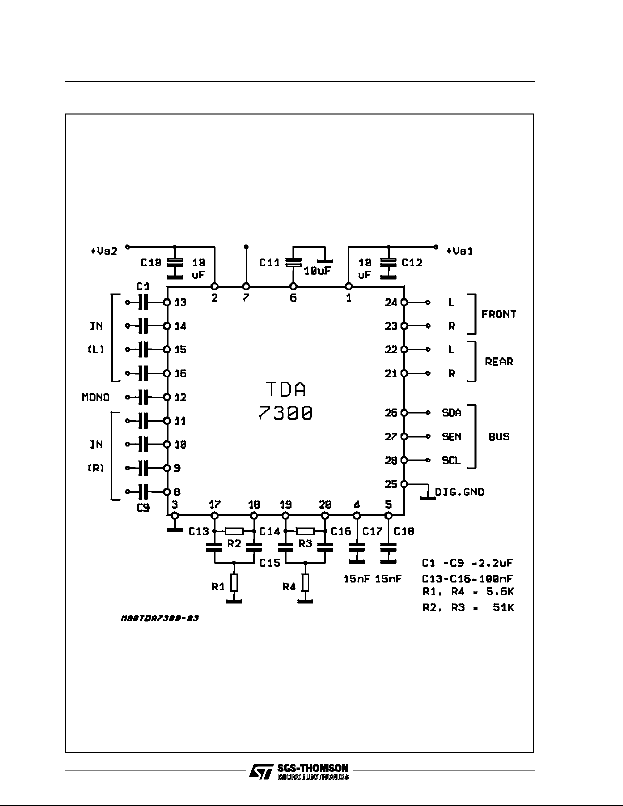
Figure1: ApplicationCircuit
4/16
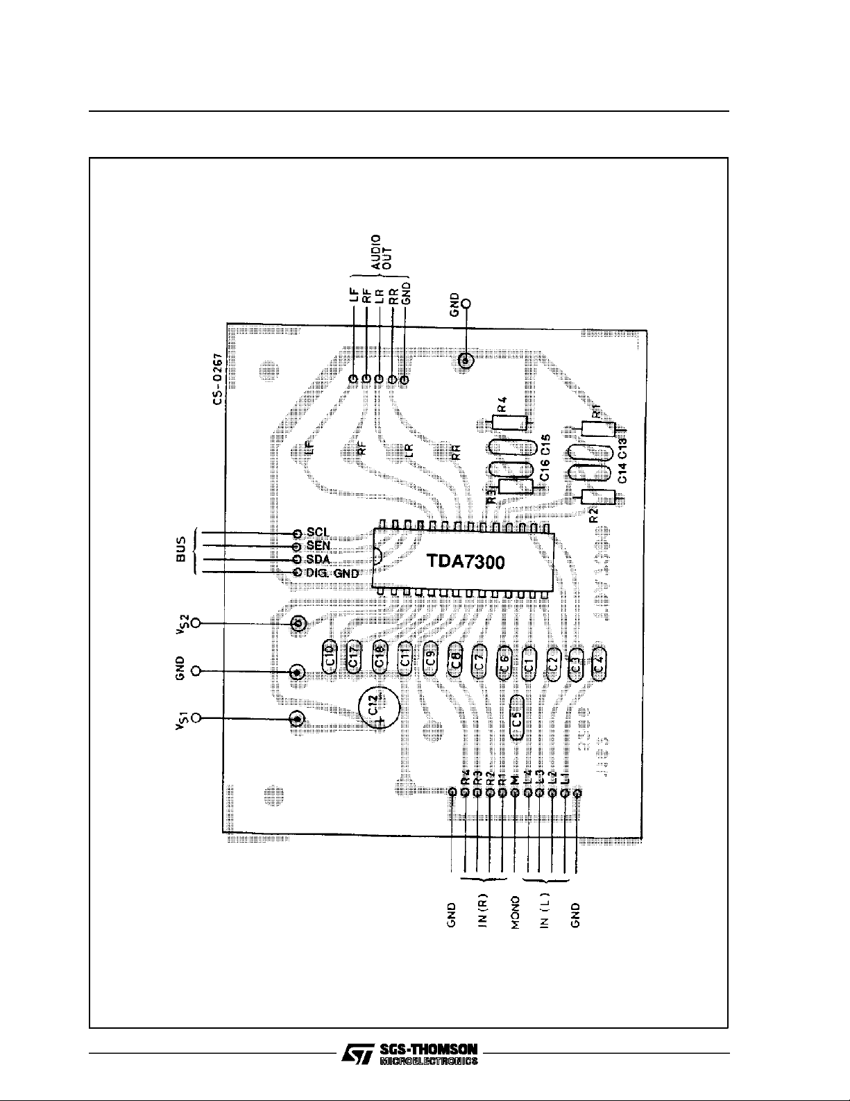
Figure2: P.C. Board and ComponentsLayout of theFig.1 (1:1scale)
TDA7300
5/16
 Loading...