

28W Hi-Fi AUDIO POWER AMPLIFIER
SUPPLYVOLTAGERANGEUP TO ±22V
SPLIT SUPPLY OPERATION
HIGHOUTPUT POWER
(UP TO 28W MUSICPOWER)
LOW DISTORTION
MUTE/STAND-BY FUNCTION
NO SWITCH ON/OFF NOISE
AC SHORT CIRCUIT PROTECTION
THERMALSHUTDOWN
ESDPROTECTION
DESCRIPTION
The TDA7298 is a monolithic integrated circuit in
Heptawatt package, intended for use as audio
class AB amplifier in TV or Hi-Fi field application.
Thanks to the wide voltage range and to the high
out current capability it’s able to supply the high-
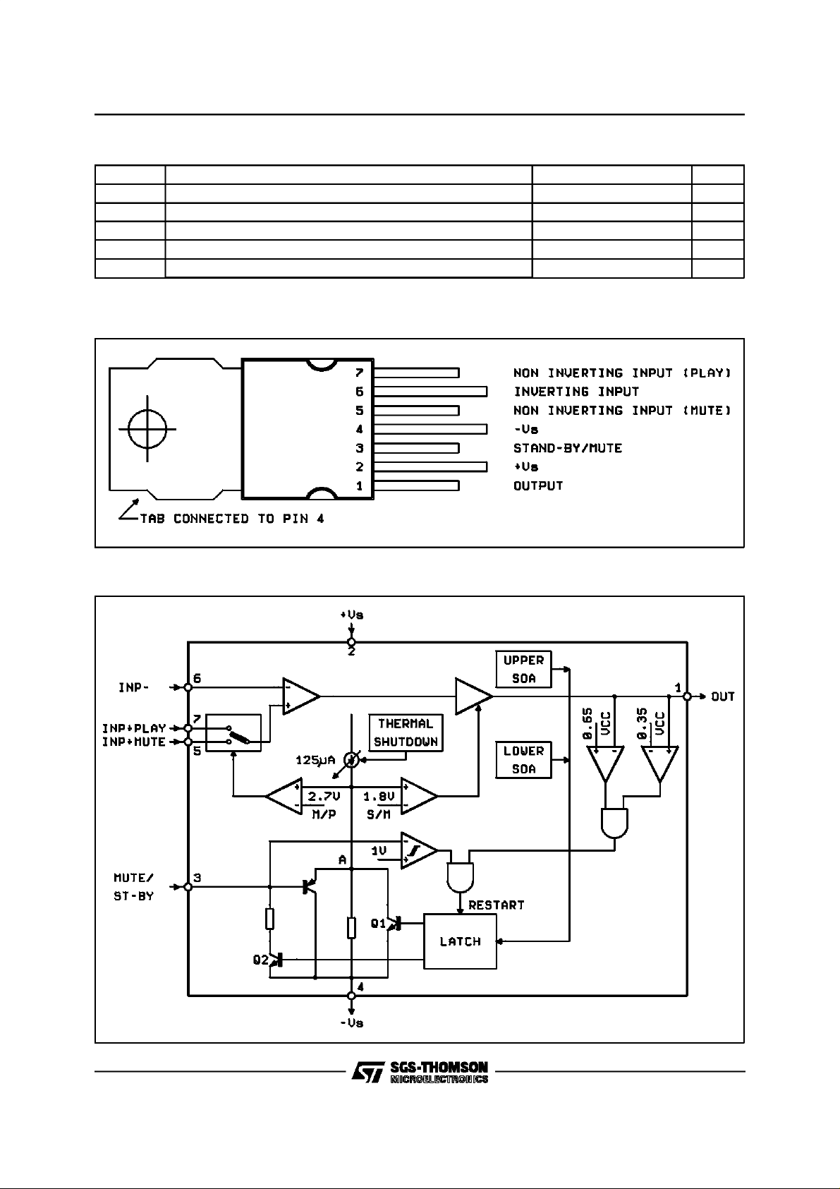
TEST AND APPLICATION CIRCUIT
TDA7298
WITH MUTE / STAND-BY
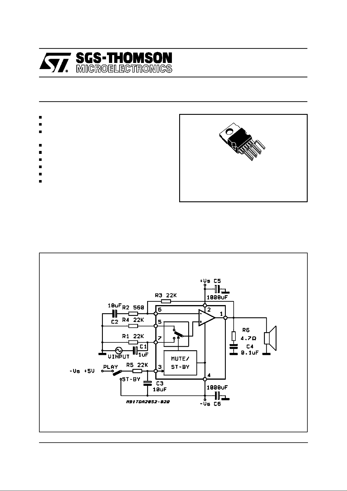
Heptawatt
ORDERING NUMBER: TDA7298
est power into both 4Ωand 8Ωloads even in
presenceof poorsupply regulation.
The built in Muting/Stand-by function simplifies
the remote operationsavoiding also switching onoff noises.
May 1997
1/11
TDA7298
ABSOLUTE MAXIMUM RATINGS
Symbol Parameter Value Unit
V
I
O
P
tot
T
op
T
stg,Tj
PIN CONNECTION (Topview)
DC Supply Voltage ±22 V
S
Output PeakCurrent (internally limited) 4 A
Power DissipationT
=70°C30W
case
Operating Temperature Range 0 to +70 °C
Storage and Junction Temperature -40 to +150 °C
BLOCK DIAGRAM
2/11
TDA7298
THERMAL DATA
Symbol Description Value Unit
R
th j-case
Thermal Resistance Junction-case Max 2.5
C/W
°
ELECTRICAL CHARACTERISTICS (Refer to the test circuit, GV= 32dB; VS+ 18V; f = 1KHz; T
25°C, unlessotherwisespecified.)
Symbol Parameter Test Condition Min. Typ. Max. Unit
V
S
I
q
I
b
V
OS
I
OS
P
O
P
O
Supply Range +6 +22 V
Total Quiescent Current VS= +22V 20 40 70 mA
Input Bias Current +0.5
Input Offset Voltage +15 mV
Input Offset Current +200 nA
Music Output Power
IEC268-3 Rules (*)
VS= + 20, RL=8Ω,
d = 10%, t = 1s
28 W
Output Power(continuous RMS) d = 10%
RL = 4Ω V
R
=8
L
Ω
= +14V
S
20
20
24
24
d=1%
R
d Total Harmonic Distortion R
=4Ω VS= +14V
L
R
=8Ω
L
=4ΩVS= +14V
L
P
= 0.1 to 10W;
O
f = 100Hz to 15KHz
=8Ω
R
L
P
= 0.1 to 10W;
O
f = 100Hz to 15KHz
17
17
0.1
0.1
0.7
0.5
SR Slew Rate 3 5 V/µs
G
V
e
N
R
SVR Supply Voltage Rejection f = 100Hz, V
T
S
Open Loop Voltage Gain 80 dB
Total Input Noise A Curve
f = 20Hz to 20KHz
Input Resistance 500 KΩ
i
ripple =1VRMS 40 50 dB
2
310
Thermal Shutdown 145
MUTE/STAND-BY FUNCTION (Ref. –VS)
=
amb
A
µ
W
W
W
W
%
%
µV
V
µ
C
°
VT
ST-BY
VT
PLAY
I
q ST-BY
ATT
ST-BY
I
pin3
Note (*):
MUSIC POWER CONCEPT
MUSIC POWER is ( according tothe IECclauses n.268-3of Jan 83) the maximalpowerwhichtheamplifier is capable of producingacrossthe
rated load resistance (regardless of non linearity) 1 sec after the application of a sinusoidalinput signal of frequency 1KHz.
According to this definition our method of measurement comprises the following steps:
1) Set the voltage supply at the maximumoperatingvalue -10%
2) Apply a input signal in the formofa 1KHz tone burst of 1 sec duration; the repetition period of the signal pulses is > 60 sec
3) The output voltage is measured 1 sec from the start of the pulse
4) Increase the input voltage until the outputsignal show a THD = 10%
5) The music power is thenV
The target of this method isto avoidexcessive dissipation in theamplifier.
Stand-by - Threshold 1 1.8 V
Play Threshold 2.7 4 V
Quiescent Current @ Stand-by V
= 0.5V 1 3 mA
pin 3
Stand-by Attenuation 70 90 dB
Pin 3 Current @ Stand-by –1 +10
2
/R1,where V
out
istheoutputvoltage measured in the condition of point 4) and R1 is the rated load impedance
out
µ
A
3/11
TDA7298
APPLICATIONS SUGGESTIONS (See Testand ApplicationCircuit)
The recommended values of the externalcomponents are those shown on the application circuit. Different values can be used;the followingtable can help the designer.
Comp. Value Purpose Larger Than Smaller Than
Ω
R1 22K
R2 560Ω Closed LoopGain set to
R3 22K
R4 22K
R5 22K
R6 4.7Ω Frequency Stability Danger of oscillations Danger of oscillations
C1 1µF Input DC Decoupling Higher Low-frequency
C2 10µF Feedback DC Decoupling Higher Low-frequency
C3 10µF Stand-by Time Constant
C4 0.100µF Frequency Stability Danger of Oscillations
C5, C6 1000µF Supply Voltage Bypass
(*) R1 = R3= R4 for POP optimization
(**) Closed Loop Gain hasto be ≥ 30dB
(*) Input Impedance Increase of Input
(*) Increase of Gain Decrease of Gain
Ω
Ω
(*) Input Impedance @ Mute
Ω
32dB (**)
Stand-by Time Constant
Impedance
Decrease of Gain Increase of Gain
Decrease of Input
Impedance
cut-off
cut-off
TYPICALCHARACTERISTICS
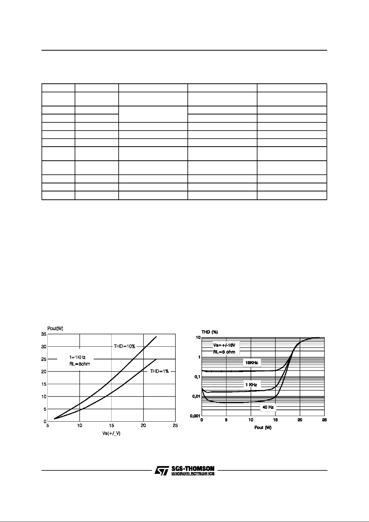
Figure 1: OutputPower vs. Supply Voltage
4/11
Figure2: Distortionvs. Output Power

Figure 3: OutputPower vs. Supply Voltage. Figure 4: Distortionvs. OutputPower.
TDA7298
Figure 5: Distortionvs. Frequency.
Figure 7: QuiescentCurrent vs. Supply Voltage
Figure6: Distortionvs. Frequency.
Figure8: SupplyVoltage Rejectionvs.Frequency.
5/11

TDA7298
Figure 9: Bandwidth.
Figure 11: Total Power Dissipation& Efficiency
vs. OutputPower.
Figure10: OutputAttenuation & Quiescent Cur-
rent vs. V
pin3
.
Figure12: Total Power Dissipation & Efficiency
vs. Output Power.
6/11

Figure 13: P.C.Board and Components Layoutof the Circuit of Fig. 14 (1:1scale)
TDA7298
Figure 14: Demo Board Schematic.
7/11

TDA7298
MUTE/STAND-BY FUNCTION
The pin 3 (MUTE/STAND-BY) controls the amplifier status by three different thresholds, referred
to-V
S.
When its voltage is lower than the first threshold
(1V, with a +70mVhysteresis), the amplifier is in
STAND-BY and all the final stage current gener-
Figure 15.
ators are off. Only the input MUTE stage is on in
orderto prevent pop-on problems.
At V
=1.8V the final stage current generators
pin3
are switched on and the amplifier operates in
MUTE.
For V
=2.7V the amplifier is definitely on
pin3
(PLAYcondition)
8/11

TDA7298
SHORT-CIRCUIT PROTECTION
The TDA7298 has an original circuit which protects the device during accidental short-circuit between output and GND / -Vs / +Vs, taking it in
STAND-BY mode, so limiting also dangerous DC
current flowing throught the loudspeaker.
If a short-circuit or an overload dangerous for the
final transistors are detected, the concernedSOA
circuit sends out a signal to the latching circuit
(with a 10µs delay time that prevents fast random
spikes from inadvertently shutting the amplifier
off) which makes Q
Diagram). Q
immediatelyshort-circuits to ground
1
and Q2saturate (see Block
1
the A point turning the final stage off while Q
short-circuits to ground the external capacitor
driving the pin 3 (Mute/Stand-by) towards zero
potential.
Only when the pin 3 voltage becomes lower than
1V, the latching circuit is allowed to reset itself
and restart the amplifier, provided that the shortcircuit condition has been removed.In fact, a window comparator is present at the output and it is
aimed at preventingthe amplifier from restarting if
the output voltageis lowerthan 0.35 Total Supply
Voltage or higher than 0.65 Total Supply Voltage.
If the output voltage lies between these two
thresholds, one may reasonably suppose the
short-circuit has been removed and the amplifier
may start operating again.
The PLAY/MUTE/STAND-BY function pin (pin 3)
is both ground- and positive supply-compatible
and can be interfaced by means of the R
5,C3
net
either to a TTL or CMOS output (µ-Processor) or
to a specificapplicationcircuit.
The R
net is fundamental, because connect-
5,C3
ing this pin directly to a low output impedance
driver such as TTL gate would prevent the correct
operation during a short-circuit. Actually a final
stage overload turns on the protection latching
circuit that makes Q
try to drivethe pin 3 voltage
2
under 0.8 V. Since the maximum current this pin
can stand is 3 mA, one must make sure the following condition is met:
THERMAL PROTECTION
The thermal protection operates on the 125µA
current generator, linearly decreasing its value
from 90°C on. By doing this, the A voltage slowly
decreases thus switching the amplifier first to
MUTE (at 145°C) and then to STAND-BY
(155°C).
Figure16: ThermalProtectionBlockDiagram
2
The maximum allowable power dissipation depends on the size of the external heatsink (thermal resistance case-ambient); figure 17 shows
the dissipable power as a function of ambient
temperaturefor differentthermalresistance.
Figure17: MaximumAllowablePower Dissipa-
tion vs. AmbientTemperature.
− 0.7V)
(V
A
≥
R
that yields: R
5
5, min
3mA
= 1.5KΩwithVA=5V.
In order to prevent pop-on and -off transients,it is
advisable to calculate the C
,R5net in such a
3
way that the STAND-BY/MUTE and MUTE/PLAY
threshold crossing slope (positive at the turn-on
and vice-versa)isless than100 V/sec.
9/11

TDA7298
HEPTAWATT PACKAGEMECHANICAL DATA
DIM.
A 4.8 0.189
C 1.37 0.054
D 2.4 2.8 0.094 0.110
D1 1.2 1.35 0.047 0.053
E 0.35 0.55 0.014 0.022
F 0.6 0.8 0.024 0.031
F1 0.9 0.035
G 2.41 2.54 2.67 0.095 0.100 0.105
G1 4.91 5.08 5.21 0.193 0.200 0.205
G2 7.49 7.62 7.8 0.295 0.300 0.307
H2 10.4 0.409
H3 10.05 10.4 0.396 0.409
L 16.97 0.668
L1 14.92 0.587
L2 21.54 0.848
L3 22.62 0.891
L5 2.6 3 0.102 0.118
L6 15.1 15.8 0.594 0.622
L7 6 6.6 0.236 0.260
M 2.8 0.110
M1 5.08 0.200
Dia 3.65 3.85 0.144 0.152
MIN. TYP. MAX. MIN. TYP. MAX.
mm inch
10/11

TDA7298
Information furnished is believed to be accurate and reliable. However, SGS-THOMSON Microelectronics assumes no responsibility for the
consequences of use of such information nor for any infringement of patents or other rights of third parties which may result from its use. No
license is granted by implication or otherwise under any patent or patent rights of SGS-THOMSON Microelectronics. Specifications mentioned in this publication are subject to change without notice. This publication supersedes and replaces all information previously supplied.
SGS-THOMSON Microelectronics products are not authorized for use as critical components in life support devices or systems without express written approval of SGS-THOMSONMicroelectronics.
1997SGS-THOMSON Microelectronics - All Rights Reserved
HEPTAWATTis a Trademark of companies belonging to the SGS-THOMSONMicroelectronics Group
SGS-THOMSON Microelectronics GROUP OF COMPANIES
Australia - Brazil - Canada - China - France - Germany - HongKong - Italy - Japan - Korea - Malaysia - Malta - Morocco -The Netherlands -
Singapore - Spain - Sweden- Switzerland- Taiwan - Thailand - UnitedKingdom - U.S.A.
11/11
 Loading...