

SGS Thomson Microelectronics TDA7297 Datasheet
TDA7297
15+15W DUAL BRIDGE AMPLIFIER
WIDESUPPLYVOLTAGERANGE(6V -18V)
MINIMUMEXTERNALCOMPONENTS
– NOSWR CAPACITOR
– NOBOOTSTRAP
– NOBOUCHEROTCELLS
– INTERNALLYFIXEDGAIN
STAND-BY & MUTEFUNCTIONS
SHORTCIRCUITPROTECTION
THERMALOVERLOADPROTECTION
DESCRIPTION
The TDA7297 is a dual bridge amplifier specially
designed for TV and PortableRadio applications.
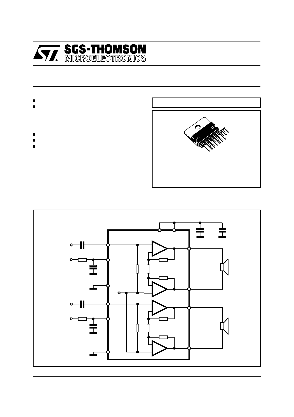
BLOCK AND APPLICATION DIAGRAM
0.22µF
IN1
ST-BY 7
4
TECHNOLOGYBI20II
Multiwatt 15
ORDERING NUMBER: TDA7297
V
CC
133
+
-
1
470µF 100nF
OUT1+
May 1997
S-GND
0.22µF
IN2
MUTE 6
PW-GND
9
12
8
Vref
15
14
2
OUT1-
OUT2+
OUT2-
D94AU175B
1/9
-
+
+
-
-
+
TDA7297
ABSOLUTE MAXIMUM RATINGS
Symbol Parameter Value Unit
V
I
P
T
T
stg,Tj
THERMAL DATA
Symbol Description Value Unit
R
th j-case
Supply Voltage 20 V
S
Output Peak Current (internally limited) 2 A
O
Total Power Dissipation (T
tot
Operating Temperature 0 to 70
op
=70°C) 33 W
case
Storage and Junction Temperature -40 to +150 °C
Thermal Resistance Junction to case Typ. 1.4 Max. 2
°
C/W
°
C
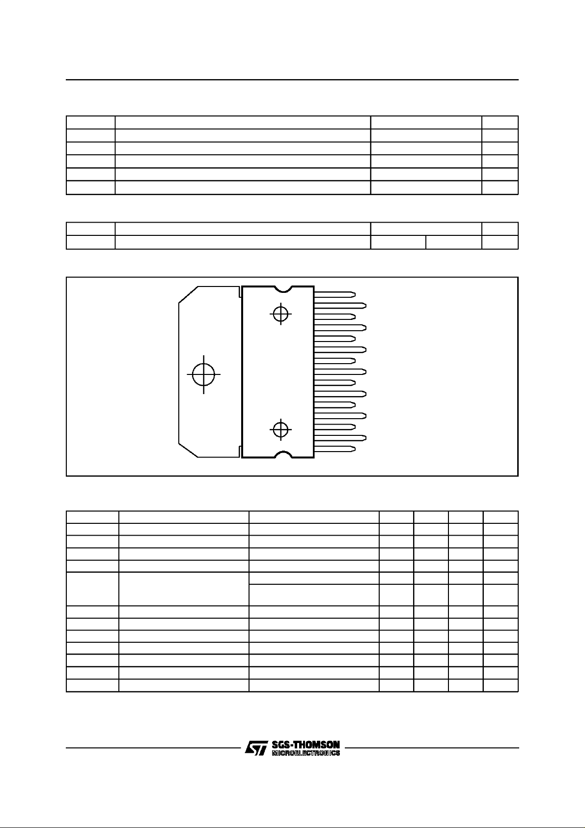
PIN CONNECTION
ELECTRICAL CHARACTERISTICS (VCC= 16.5V, RL=8Ω, f = 1kHz, T
(Top view)
15
14
13
12
11
10
9
8
7
6
5
4
3
2
1
D95AU261
OUT2+
OUT2VCC
IN2
N.C.
N.C.
S-GND
PW-GND
ST-BY
MUTE
N.C.
IN1
V
CC
OUT1OUT1+
amb
=25°C unless otherwise
specified.)
Symbol Parameter Test Condition Min. Typ. Max. Unit
V
CC
I
q
V
OS
P
O
THD Total Harmonic Distortion P
SVR Supply Voltage Rejection f = 100Hz V
CT Crosstalk 46 60 dB
A
MUTE
T
W
G
V
∆Gv Voltage Gain Matching 0.5 dB
R
Supply Range 6.5 18 V
Total Quiescent Current RL= ∞ 50 65 mA
Output Offset Voltage 120 mV
Output Power THD = 10% 13 15 W
= 1W 0.1 0.3 %
O
P
= 0.1W to 5W
O
f = 100Hz to 15kHz
= 0.5V 40 56 dB
R
Mute Attenuation 60 80 dB
Thermal Threshold 150 °C
Closed Loop Voltage Gain 31 32 33 dB
Input Resistance 25 30 K
i
1%
Ω
2/9
TDA7297
ELECTRICALCHARACTERISTICS
Symbol Parameter Test Condition Min. Typ. Max. Unit
VT
VT
MUTE
ST-BY
I
ST-BY
e
N
Mute Threshold VO= -30dB 2.3 2.9 4.1 V
St-by Threshold 0.8 1.3 1.8 V
ST-BY current V6 = GND 100
Total Output Noise Voltage A curve
APPLICATIONSUGGESTION
STAND-BYAND MUTE FUNCTIONS
(A) MicroprocessorApplication
In order to avoid annoying ”Pop-Noise” during
Turn-On/Off transients, it is necessary to guarantee the right St-by and mute signals sequence.
It is quite simple to obtain this functionusing a microprocessor(Fig.1 and 2).
At first St-by signal (from mP) goes high and the
voltage across the St-by terminal (Pin 7) starts to
increase exponentially. The external RC network
is intended to turn-on slowly the biasing circuits of
(Continued)
f = 20Hz to 20kHz
150
220 500
the amplifier, this to avoid ”POP” and ”CLICK” on
the outputs.
When this voltage reaches the St-by threshold
level, the amplifier is switched-onand the external
capacitors in series to the input terminals (C3,
C5) start to charge.
It’s necessaryto mantain the mute signal low until
the capacitors are fully charged, this to avoid that
the device goes in play mode causing a loud ”Pop
Noise”on the speakers.
A delay of 100-200ms between St-by and mute
signals is suitable for a properoperation.
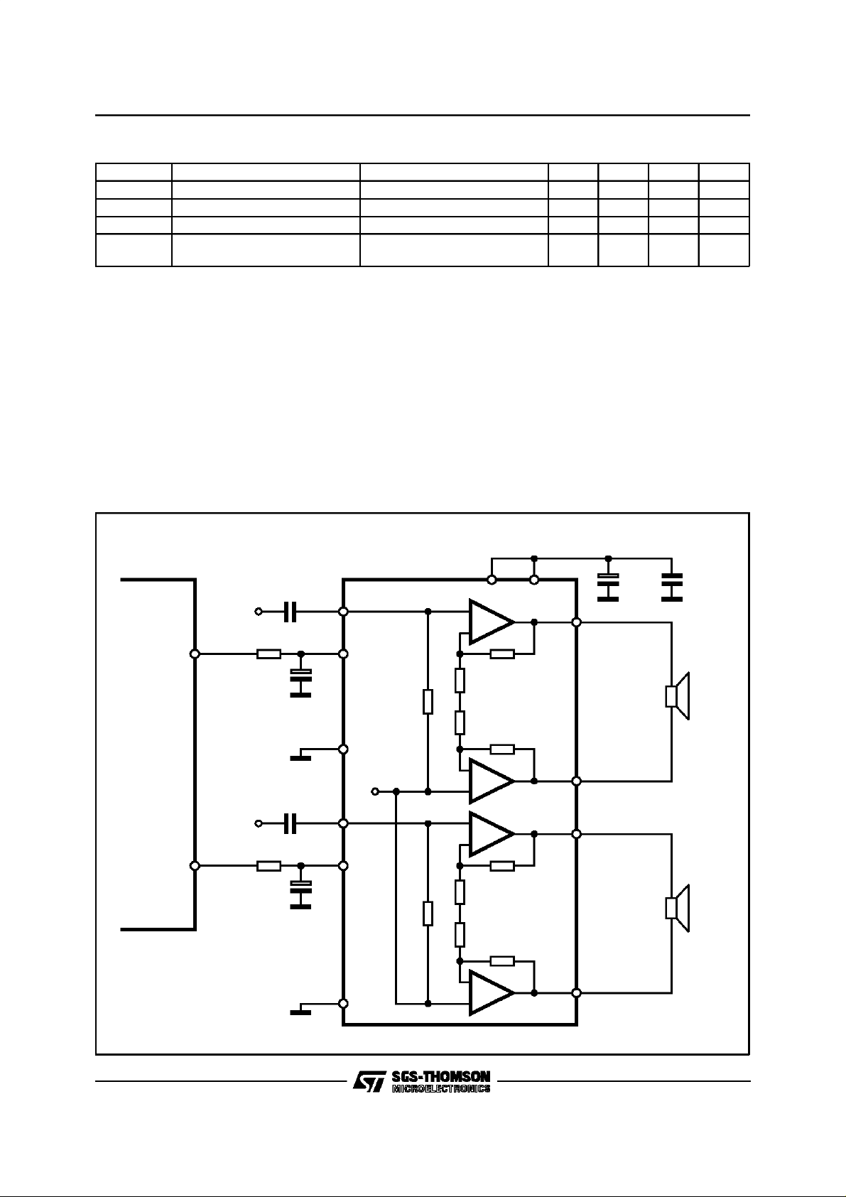
Figure 1: MicroprocessorApplication
V
CC
µ
µ
µV
A
V
µP
IN1
ST-BY
IN2
MUTE
C1 0.22µF
R1 10K
C2
10µF
C3 0.22µF
R2 10K
C4
1µF
PW-GND
S-GND
4
7
9
12
6
8
Vref
133
15
14
1
OUT1+
2
OUT1-
OUT2+
OUT2-
+
-
-
+
+
-
-
+
C5
470µF
D95AU258A
C6
100nF
3/9
 Loading...