

TDA7296A
70V - 60W DMOS AUDIO AMPLIFIER WITH MUTE/ST-BY
PRODUCT PREVIEW
VERY HIGH OPERATING VOLTAGE RANGE
(±35V)
DMOSPOWERSTAGE
HIGH OUTPUT POWER (UP TO 60W MUSIC
POWER)
MUTING/STAND-BYFUNCTIONS
NO SWITCH ON/OFFNOISE
NO BOUCHEROTCELLS
VERYLOW DISTORTION
VERYLOW NOISE
SHORTCIRCUITPROTECTION
THERMALSHUTDOWN
CLIPPINGDETECTION OUTPUT
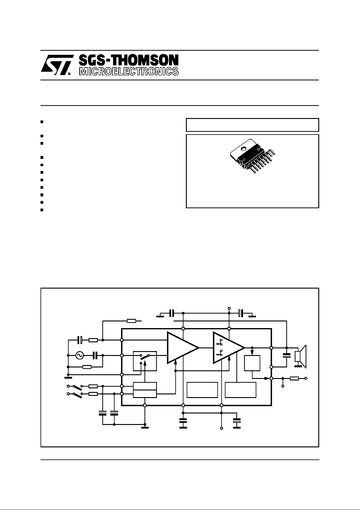
DESCRIPTION
The TDA7296A is a monolithic integrated circuit
in Multiwatt15 package, intended for use as audio
class AB amplifier in Hi-Fi field applications
(Home Stereo, self powered loudspeakers, Topclass TV). Thanks to the wide voltage range and
to the high out current capability it is able to supply the highest power into both 4Ω and 8Ω loads
Figure 1: Typical Applicationand Test Circuit
MULTIPOWER BCD TECHNOLOGY
Multiwatt 15
ORDERING NUMBER: TDA7296AV
even in presence of poor supply regulation, with
high Supply Voltage Rejection.
The built in muting function with turn on delay
simplifiesthe remote operation avoidingswitching
on-off noises.
The device provides a circuit for the detection of
clipping in the output stages. The output, on open
collector, is able to drive system with automatic
levelcontrol.
+VsC7 100nF C6 1000µF
R3 22K
+PWVs+Vs
CD
S/C
PROTECTION
158
-Vs
VM
VSTBY
C2
R2
22µF
680Ω
C1 470nF
R1 22K
R5 10K
R4 22K
C3 10µFC410µF
IN- 2
IN+
IN+MUTE
MUTE
STBY
3
4
10
9
MUTE
STBY
1
STBY-GND
713
-
+
THERMAL
SHUTDOWN
-Vs -PWVs
C9 100nF C8 1000µF
June 1996
This is preliminaryinformationon a new productnow in development. Details aresubject to change withoutnotice.
14
6
5
D96AU494
OUT
C5
22µF
BOOTSTRAP
+5V
1/13
TDA7296A
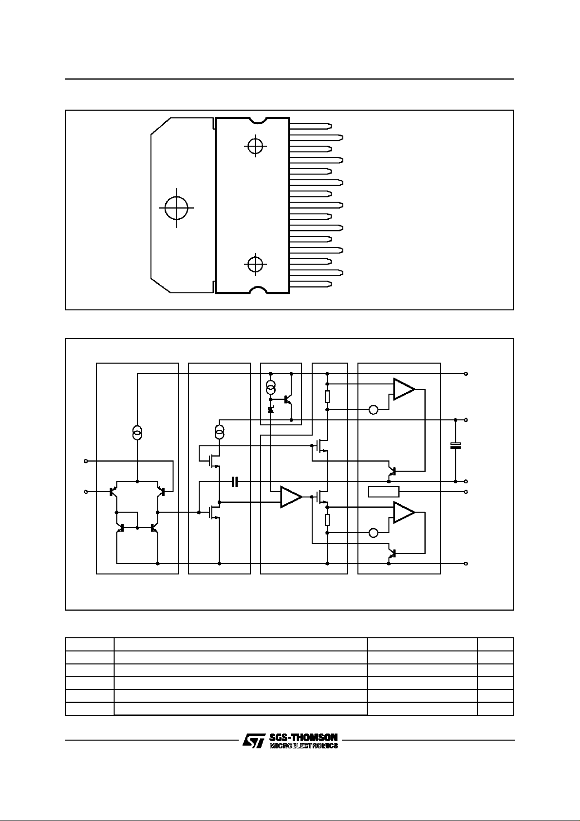
PIN CONNECTION (Topview)
BLOCK DIAGRAM
15
14
13
12
11
10
9
8
7
6
5
4
3
2
1
BOOTSTRAP
D96AU495
-V
(POWER)
S
OUT
+V
(POWER)
S
N.C.
N.C.
MUTE
STAND-BY
(SIGNAL)
-V
S
+V
(SIGNAL)
S
BOOTSTRAP
CD
SVR
NON INVERTING INPUT
INVERTING INPUT
STAND-BY GND
+
-
+
+V
S
BOOTSTRAP
IN+
OUTPUT
IN-
BIPOLAR
TRANSCONDUCTANCE
INPUT STAGE
MOS GAIN &
LEVEL SHIFTING
STAGE
MOS OUTPUT STAGE SHORT CIRCUIT
CD
+
-
+
PROTECTION
CD
-V
D96AU496
ABSOLUTE MAXIMUM RATINGS
Symbol Parameter Value Unit
V
I
O
P
tot
T
op
T
stg,Tj
Supply Voltage
S
Output Peak Current 5 A
Power Dissipation T
=70°C50W
case
Operating Ambient Temperature Range 0 to 70
Storage and Junction Temperature 150
2/13
35 V
±
S
C
°
C
°
TDA7296A
THERMAL DATA
Symbol Description Value Unit
R
th j-case
Thermal Resistance Junction-case Max 1.5
C/W
°
ELECTRICALCHARACTERISTICS
R
=50Ω;T
g
=25°C,f = 1 kHz; unlessotherwisespecified.
amb
(Refer to the Test Circuit V
= ±24V, RL=8Ω,GV= 30dB;
S
Symbol Parameter Test Condition Min. Typ. Max. Unit
V
I
I
V
I
OS
P
Operating Supply Range ±10 ±35 V
S
Quiescent Current 20 30 60 mA
q
Input Bias Current 500 nA
b
Input Offset Voltage +10 mV
OS
Input Offset Current +100 nA
RMS Continuous Output Power d = 0.5%:
O
Music Power (RMS) (*)
t=1s
∆
d Total Harmonic Distortion (**) P
V
=±24V,RL=8
S
V
=±21V, RL=6Ω
S
ς
=±18V, RL=4Ω
S
Ω
d = 10%;
R
=8Ω ;VS=±29V
L
R
=6Ω ;VS=±24V
L
R
=4Ω;VS=±22V
L
= 5W; f = 1kHz
O
P
=0.1to 20W; f= 20Hzto20kHz
O
=±18V, RL=4
V
S
P
= 5W; f = 1kHz
O
P
=0.1to 20W; f= 20Hzto20kHz
O
Ω:
27
27
27
30
30
30
60
60
60
0.005
0.01
0.1
0.1
W
W
W
W
W
W
%
%
%
%
SR Slew Rate 7 10 V/µs
G
G
e
f
L,fH
R
SVR Supply Voltage Rejection f = 100Hz; V
T
STAND-BY FUNCTION (Ref: -V
V
ST on
V
ST off
ATT
I
q st-by
MUTE FUNCTION (Ref: -V
V
Mon
V
Moff
ATT
DC Off Clipping detector OFF.
Open Loop Voltage Gain 80 dB
V
Closed Loop Voltage Gain 24 30 40 dB
V
Total Input Noise A = curve
N
f = 20Hz to 20kHz
1
25
Frequency Response (-3dB) PO= 1W 20Hz to 20kHz
Input Resistance 100 kΩ
i
= 0.5Vrms 60 75 dB
ripple
Thermal Shutdown 145
S
or GND)
S
Stand-by on Threshold 1.5 V
Stand-by off Threshold 3.5 V
Stand-by Attenuation 70 90 dB
st-by
Quiescent Current @ Stand-by 1 3 mA
or GND)
S
Mute on Threshold 1.5 V
Mute off Threshold 3.5 V
Mute AttenuatIon 60 80 dB
mute
THD = 1% TBD %
µV
V
µ
C
°
CD output Duty Cycle
DC On Clipping detector On.
THD = 10% TBD %
CD output Duty Cycle
Note (*):
MUSIC POWERis the maximalpower which the amplifieris capableof producing across therated load resistance (regardless ofnon linearity)
1 sec after the applicationofasinusoidalinput signal of frequency 1KHz.
Note (**): Tested with optimized ApplicationBoard (see fig. 2)
3/13
TDA7296A
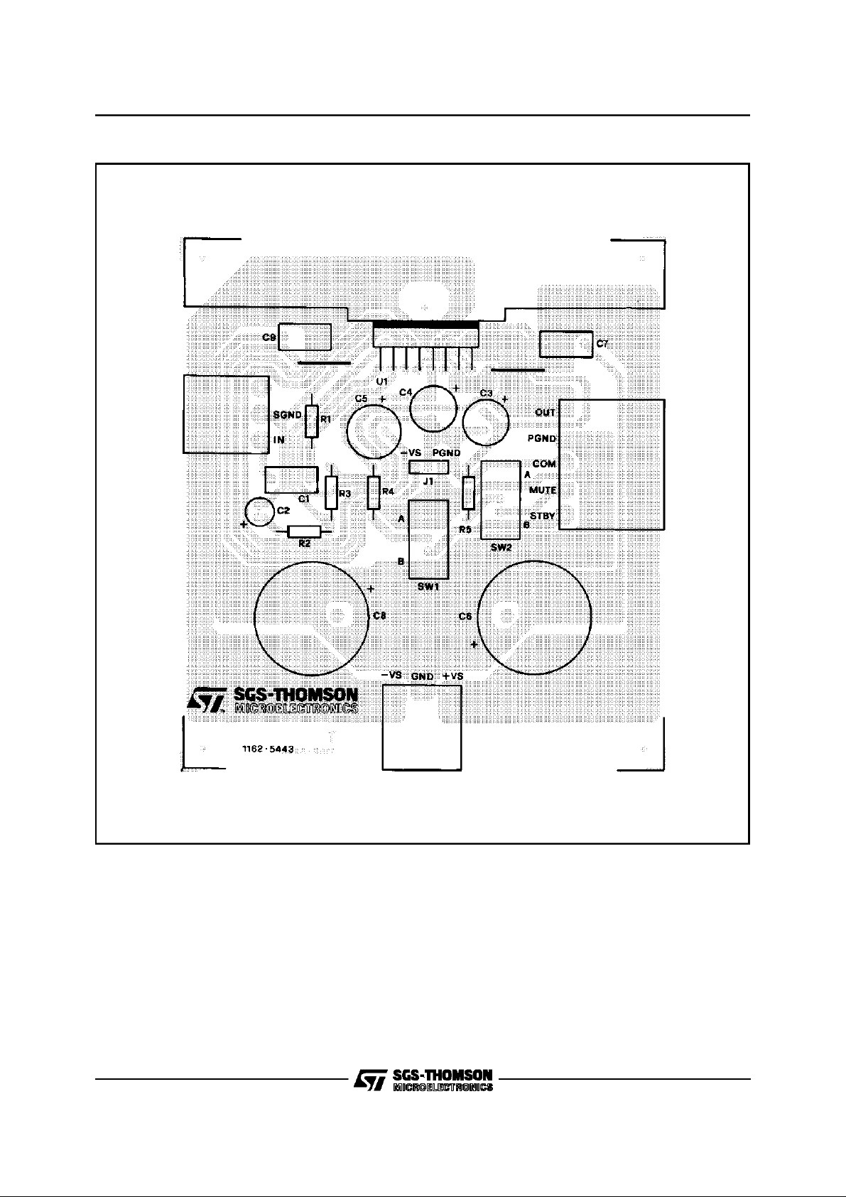
Figure 2:
P.C.B.and componentslayout of thecircuit of figure 1. (1:1 scale)
TDA7296A
Note:
The Stand-by and Mute functions canbe referred eitherto GND or -VS.
On the P.C.B. is possibletosetboth the configuration throughthe jumperJ1.
4/13

TDA7296A
APPLICATIONSUGGESTIONS(seeTestand Application Circuitsof the Fig. 1)
The recommended values of the external components are those shown on the application circuit of Figure 1. Different values can be used;the following table can help the designer.
COMPONENTS SUGGESTED VALUE PURPOSE
R1 (*) 22k INPUT RESISTANCE INCREASE INPUT
R2 680
R3 (*) 22k INCREASE OF GAIN DECREASE OF GAIN
R4 22k ST-BY TIME
R5 10k MUTE TIME
C1 0.47µF INPUT DC
C2 22µF FEEDBACK DC
C3 10µF MUTE TIME
C4 10µF ST-BY TIME
Ω
CLOSED LOOP GAIN
SET TO 30dB (**)
CONSTANT
CONSTANT
DECOUPLING
DECOUPLING
CONSTANT
CONSTANT
LARGER THAN
SUGGESTED
IMPRDANCE
DECREASE OF GAIN INCREASE OF GAIN
LARGER ST-BY
ON/OFF TIME
LARGER MUTE
ON/OFF TIME
LARGER MUTE
ON/OFF TIME
LARGER ST-BY
ON/OFF TIME
SMALLER THAN
SUGGESTED
DECREASE INPUT
IMPEDANCE
SMALLER ST-BY
ON/OFF TIME;
POP NOISE
SMALLER MUTE
ON/OFF TIME
HIGHER LOW
FREQUENCY
CUTOFF
HIGHER LOW
FREQUENCY
CUTOFF
SMALLER MUTE
ON/OFF TIME
SMALLER ST-BY
ON/OFF TIME;
POP NOISE
C5 22µF BOOTSTRAPPING SIGNAL
C6, C8 1000µF SUPPLY VOLTAGE
C7, C9 0.1µF SUPPLY VOLTAGE
(*) R1 = R3 FOR POP OPTIMIZATION
(**) CLOSED LOOP GAINHAS TO BE≥24dB
BYPASS
BYPASS
DEGRADATION AT
LOW FREQUENCY
DANGER OF
OSCILLATION
DANGER OF
OSCILLATION
5/13

TDA7296A
TYPICALCHARACTERISTICS
(ApplicationCircuit of fig 1 unless otherwise specified)
Figure 3:
OutputPowervs. Supply Voltage.
Figure 5: OutputPower vs. Supply Voltage
Figure4:
Distortionvs. Output Power
Figure6: Distortionvs.OutputPower
Figure 7: Distortionvs.Frequency
6/13
Figure8: Distortionvs.Frequency

TYPICALCHARACTERISTICS (continued)
TDA7296A
Figure 9:
Figure 11:
QuiescentCurrent vs. Supply Voltage
MuteAttenuationvs. V
pin10
Figure10:
SupplyVoltageRejectionvs.Frequency
Figure12: St-byAttenuationvs. V
pin9
Figure 13: Power Dissipationvs. OutputPower
Figure14:
PowerDissipation vs. OutputPower
7/13

TDA7296A
INTRODUCTION
In consumer electronics, an increasing demand
has arisen for very high power monolithic audio
amplifiers able to match,with a low cost the performance obtained from the best discrete designs.
The task of realizing this linear integrated circuit
in conventional bipolar technology is made extremely difficult by the occurence of 2nd breakdown phenomenon. It limits the safe operating
area (SOA) of the power devices, and as a consequence, the maximum attainableoutput power,
especiallyin presence of highly reactive loads.
Moreover, full exploitation of the SOA translates
into a substantial increase in circuit and layout
complexity due to the need for sophisticated protection circuits.
To overcome these substantial drawbacks, the
use of power MOS devices, which are immune
monic distortion and good behaviour over frequency response; moreover, an accurate control
of quiescent current is required.
A local linearizing feedback, provided by differential amplifier A, is used to fullfilthe above requirements, allowing a simple and effective quiescent
currentsetting.
Proper biasing of the power output transistors
alone is howevernot enough to guaranteethe absenceof crossoverdistortion.
While a linearization of the DC transfer characteristic of the stage is obtained, the dynamic behaviour of thesystem must be taken into account.
A significant aid in keeping the distortion contributed by the final stage as low as possible is provided by the compensation scheme, which exploits the direct connection of the Miller capacitor
at the amplifier’s output to introduce a local AC
feedbackpathenclosing the output stage itself.
from secondarybreakdownis highly desirable.
The device described has therefore been devel-
oped in a mixed bipolar-MOS high voltage technology called BCD 80.
2) Protections
In designing a power IC, particular attention must
be reserved to the circuits devoted to protection
of the device from short circuit or overload condi-
1) OutputStage
The main design task one is confrontedwith while
developing an integrated circuit as a power operational amplifier, independently of the technology used, is that of realising the outputstage.
The solution shown as a principle schematic by
Fig 15 represents the DMOS unity-gain output
buffer of the TDA7296A.
This large-signal, high-power buffer must be capable of handling extremely high current and voltage levels while maintaining acceptably low har-
tions.
Due to the absence of the 2nd breakdown phe-
nomenon, the SOA of the power DMOS transis-
tors is delimited only by a maximum dissipation
curve dependent on the duration of the applied
stimulus.
In order to fully exploit the capabilities of the
power transistors, the protection scheme imple-
mented in this device combines a conventional
SOA protection circuit with a novel local tempera-
ture sensing technique which ” dynamically” con-
trols the maximumdissipation.
Figure 15: PrincipleSchematicof a DMOS unity-gain buffer.
8/13

Figure 16: Turn ON/OFF SuggestedSequence
+Vs
(V)
+35
-35
-Vs
VIN
(mV)
V
ST-BY
PIN #9
(V)
5V
TDA7296A
V
MUTE
PIN #10
(V)
IP
(mA)
V
OUT
(V)
5V
OFF
ST-BY
PLAY
MUTE MUTE
In addition to the overload protection described
above, the device features a thermal shutdown
circuit which initially puts the device into a muting
state (@ Tj = 145
Figure 17:
SingleSignalST-BY/MUTEControl
o
C) and then into stand-by (@
Circuit
MUTE STBY
MUTE/
ST-BY
20K
10K 30K
1N4148
10µF10µF
D93AU014
ST-BY OFF
D93AU013
o
Tj = 150
C).
Full protection against electrostatic discharges on
everypin is included.
3) OtherFeatures
The device is provided with both stand-by and
mute functions, independently driven by two
CMOSlogiccompatibleinput pins.
The circuits dedicated to the switching on and off
of the amplifier have been carefully optimized to
avoid any kindof uncontrolled audibletransient at
the output.
The sequence that we recommend during the
ON/OFFtransientsisshown by Figure 16.
The application of figure 17 shows the possibility
of using only one command for both st-by and
mute functions. On both the pins, the maximum
applicable range corresponds to the operating
supplyvoltage.
9/13

TDA7296A
4) ClippingDetectorOutput
The TDA7296A is equipped with an internal circuit able to detect the output stage saturation providing a proper current sinking into on open collector output (pin 5) when a certain distortion level
is reachedat output.
This particular function allows gain compression
facility whenever the amplifier is overdriven, thus
obtaining high quality sound all listening levels.
Figure 18:
ClippingDetectorOutput Waveform
V
O
I
CLIP
S96AU498
OUTPUT
SIGNAL
t
Figure 19: Bridge ApplicationCircuit
BRIDGEAPPLICATION
Another application suggestion is the BRIDGE
configuration, where two TDA7296A are used, as
shownby the schematic diagram of figure 19.
In this application, the value of the load must not
be lower than 8 Ohm for dissipation and current
capabilityreasons.
A suitable field of application includes HI-FI/TV
subwoofersrealizations.
The main advantagesofferedby this solution are:
- High power performanceswith limited supply
voltagelevel.
- Considerablyhigh output power even with high
loadvalues (i.e. 16 Ohm).
The characteristics shown by figures 21 and 22,
measured with loads respectively 8 Ohm and 16
Ohm.
With Rl= 8 Ohm, Vs = ±18V the maximum output
power obtainable is 60W, while with Rl=16 Ohm,
Vs = ±24V the maximumPout is 60W.
+Vs
Vi
ST-BY/MUTE
10K 30K
20K
22µF
1N4148
0.56µF 22K
22K0.56µF
2200µF0.22µF
22µF
3
1
4
10
10
3
1
4
9
9
137
+
-
15 8
+
-
137
6
22µF
14
2
815
2200µF 0.22µF
6
14
2
22K
680
22µF
22K
680
22K
-Vs
10/13
D96AU497

TDA7296A
Figure 20:
FrequencyResponseof the Bridge
Application
Figure 22: Distortionvs.OutputPower
Figure21: Distortionvs.OutputPower
11/13

TDA7296A
MULTIWATT15 PACKAGE MECHANICAL DATA
DIM.
MIN. TYP. MAX. MIN. TYP. MAX.
A 5 0.197
B 2.65 0.104
C 1.6 0.063
D 1 0.039
E 0.49 0.55 0.019 0.022
F 0.66 0.75 0.026 0.030
G 1.14 1.27 1.4 0.045 0.050 0.055
G1 17.57 17.78 17.91 0.692 0.700 0.705
H1 19.6 0.772
H2 20.2 0.795
L 22.1 22.6 0.870 0.890
L1 22 22.5 0.866 0.886
L2 17.65 18.1 0.695 0.713
L3 17.25 17.5 17.75 0.679 0.689 0.699
L4 10.3 10.7 10.9 0.406 0.421 0.429
L7 2.65 2.9 0.104 0.114
M 4.2 4.3 4.6 0.165 0.169 0.181
M1 4.5 5.08 5.3 0.177 0.200 0.209
S 1.9 2.6 0.075 0.102
S1 1.9 2.6 0.075 0.102
Dia1 3.65 3.85 0.144 0.152
mm inch
12/13

TDA7296A
Information furnished is believed to be accurate and reliable. However, SGS-THOMSON Microelectronics assumes no responsibility for the
consequences of use of such information nor for any infringement of patents or other rights of third parties which may result from its use. No
license is granted by implication or otherwise under any patent or patentrightsof SGS-THOMSON Microelectronics. Specification mentioned
in this publication are subject to change without notice. This publication supersedes and replaces all information previously supplied. SGSTHOMSON Microelectronics products are not authorized for use as critical components in life support devices or systems without express
written approval of SGS-THOMSON Microelectronics.
1996SGS-THOMSON Microelectronics– Printed in Italy– All Rights Reserved
SGS-THOMSON Microelectronics GROUPOF COMPANIES
Australia - Brazil - Canada - China - France -Germany- HongKong - Italy - Japan -Korea - Malaysia- Malta- Morocco - The Netherlands-
Singapore - Spain - Sweden -Switzerland - Taiwan - Thailand-United Kingdom- U.S.A.
13/13
 Loading...