

TDA7295
80V - 80W DMOS AUDIO AMPLIFIER WITH MUTE/ST-BY
VERY HIGH OPERATING VOLTAGE RANGE
(±40V)
DMOSPOWERSTAGE
HIGH OUTPUT POWER (UP TO 80W MUSIC
POWER)
MUTING/STAND-BYFUNCTIONS
NO SWITCH ON/OFFNOISE
NO BOUCHEROTCELLS
VERYLOW DISTORTION
VERYLOW NOISE
SHORTCIRCUITPROTECTION
THERMALSHUTDOWN
DESCRIPTION
The TDA7295 is a monolithic integrated circuit in
Multiwatt15 package, intended for use as audio
class AB amplifier in Hi-Fi field applications
(Home Stereo, self powered loudspeakers, Topclass TV). Thanks to the wide voltage range and
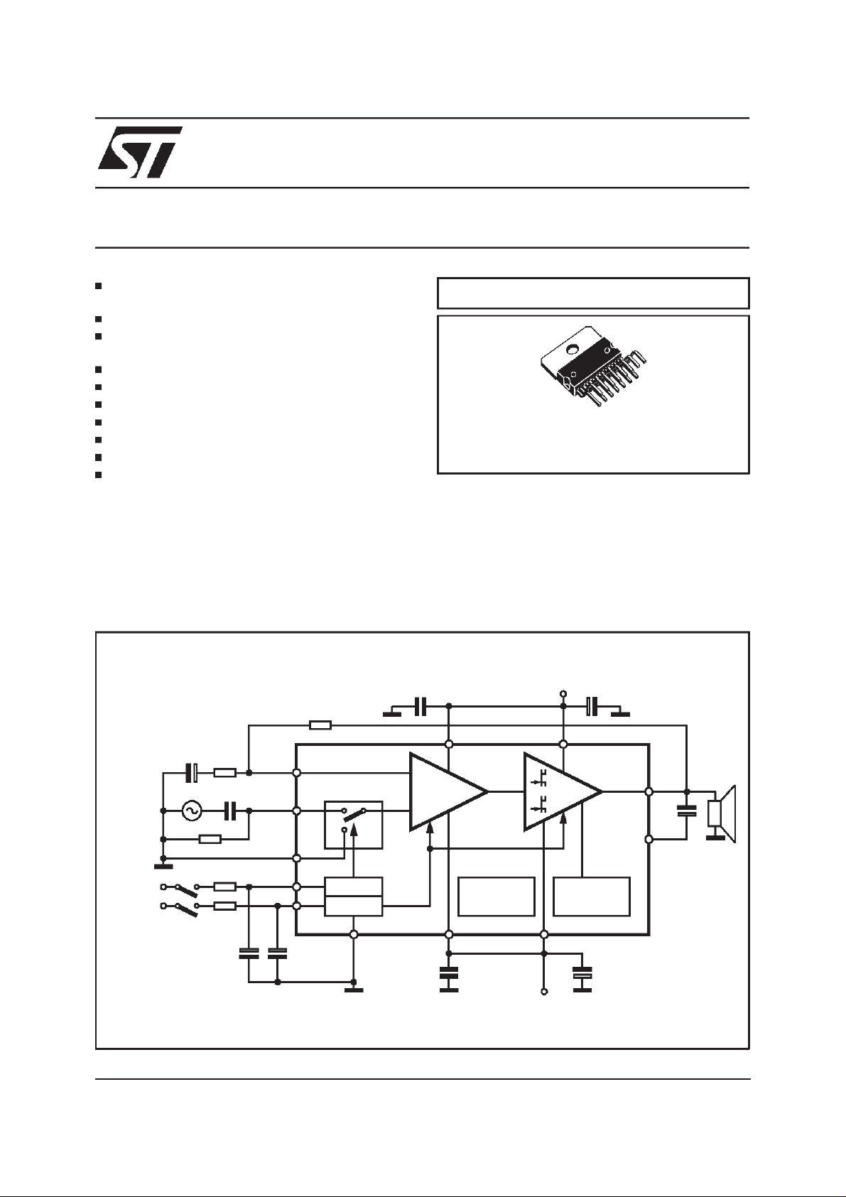
Figure 1: Typical Applicationand Test Circuit
MULTIPOWER BCD TECHNOLOGY
Multiwatt 15
ORDERING NUMBER: TDA7295V
to the high out current capability it is able to supply the highest power into both 4Ω and 8Ω loads
even in presence of poor supply regulation, with
high Supply Voltage Rejection.
The built in muting function with turn on delay
simplifiesthe remote operation avoiding switching
on-off noises.
+VsC7 100nF C6 1000µF
VM
VSTBY
July 1999
R3 22K
C2
R2
22µF
680Ω
C1 470nF
R1 22K
R5 10K
R4 22K
C3 10µFC410µF
IN- 2
IN+
IN+MUTE
MUTE
STBY
3
4
10
9
MUTE
STBY
1
STBY-GND
+PWVs+Vs
713
-
+
THERMAL
SHUTDOWN
-Vs -PWVs
C9 100nF C8 1000µF
-Vs
S/C
PROTECTION
158
14
6
OUT
C5
22µF
BOOTSTRAP
D93AU011
1/13
TDA7295
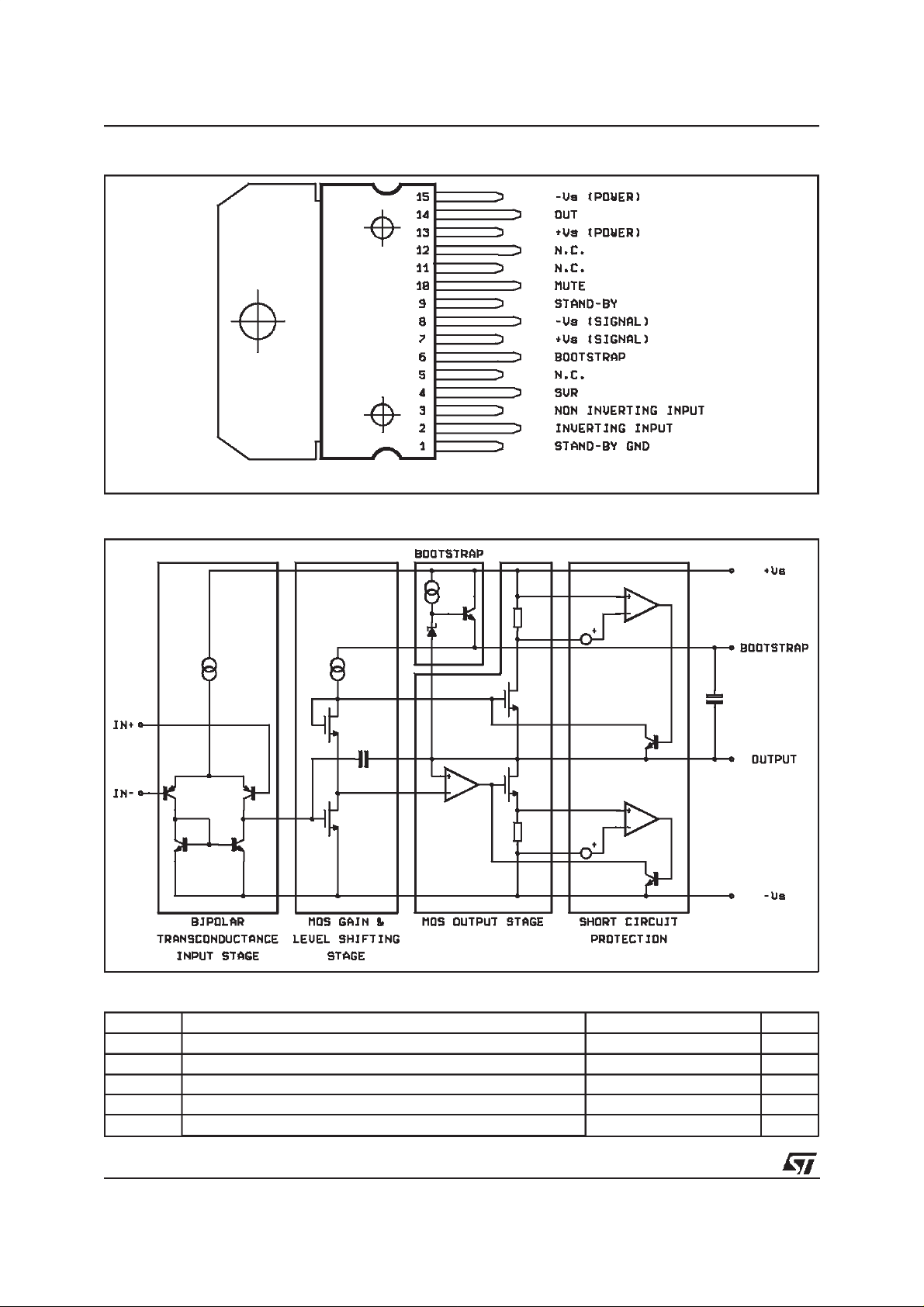
PIN CONNECTION (Topview)
BLOCK DIAGRAM
ABSOLUTE MAXIMUM RATINGS
Symbol Parameter Value Unit
V
I
O
P
tot
T
op
T
stg,Tj
Supply Voltage
S
Output Peak Current 6 A
Power Dissipation T
=70°C50W
case
Operating Ambient Temperature Range 0 to 70
Storage and Junction Temperature 150
2/13
40 V
±
C
°
C
°
TDA7295
THERMAL DATA
Symbol Description Value Unit
R
th j-case
Thermal Resistance Junction-case Max 1.5
C/W
°
ELECTRICALCHARACTERISTICS
R
=50Ω;T
g
=25°C,f = 1 kHz; unlessotherwise specified.
amb
(Refer to the Test Circuit V
= ±30V, RL=8Ω,GV= 30dB;
S
Symbol Parameter Test Condition Min. Typ. Max. Unit
V
I
I
V
I
OS
P
Operating Supply Range ±10 ±40 V
S
Quiescent Current 20 30 60 mA
q
Input Bias Current 500 nA
b
Input Offset Voltage +10 mV
OS
Input Offset Current +100 nA
RMS Continuous Output Power d = 0.5%:
O
Music Power (RMS) (*)
t=1s
∆
d Total Harmonic Distortion (**) P
V
=±30V,RL=8
S
V
=±26V, RL=6Ω
S
ς
=±22V, RL=4Ω
S
Ω
d = 10%;
R
=8Ω ;VS=±34V
L
(***) R
P
V
P
P
=4Ω;VS=±26V
L
= 5W; f = 1kHz
O
=0.1to 30W; f = 20Hzto 20kHz
O
= ±22V, RL=4Ω:
S
= 5W; f = 1kHz
O
=0.1to 30W; f = 20Hzto 20kHz
O
45
45
45
50
50
50
80
80
0.005
0.01
0.1
0.1
W
W
W
W
W
%
%
%
%
SR Slew Rate 7 10 V/µs
G
G
e
f
L,fH
R
SVR Supply Voltage Rejection f = 100Hz; V
T
STAND-BY FUNCTION (Ref: -V
V
ST on
V
ST off
ATT
I
q st-by
MUTE FUNCTION (Ref: -V
V
Mon
V
Moff
ATT
Note (*):
MUSIC POWER is the maximal power which the amplifieris capableof producing across the rated load resistance (regardless of non linearity)
1 sec after the application of a sinusoidal input signal of frequency 1KHz.
Note (**): Tested with optimized Application Board (see fig. 2)
Note (***): Limited by the max. allowable out current
Open Loop Voltage Gain 80 dB
V
Closed Loop Voltage Gain 24 30 40 dB
V
Total Input Noise A = curve
N
f = 20Hz to 20kHz
1
25
Frequency Response (-3dB) PO= 1W 20Hz to 20kHz
Input Resistance 100 k
i
= 0.5Vrms 60 75 dB
ripple
Thermal Shutdown 145 °C
S
or GND)
S
Stand-by on Threshold 1.5 V
Stand-by off Threshold 3.5 V
Stand-by Attenuation 70 90 dB
st-by
Quiescent Current @ Stand-by 1 3 mA
or GND)
S
Mute on Threshold 1.5 V
Mute off Threshold 3.5 V
Mute AttenuatIon 60 80 dB
mute
V
µ
µV
Ω
3/13
TDA7295
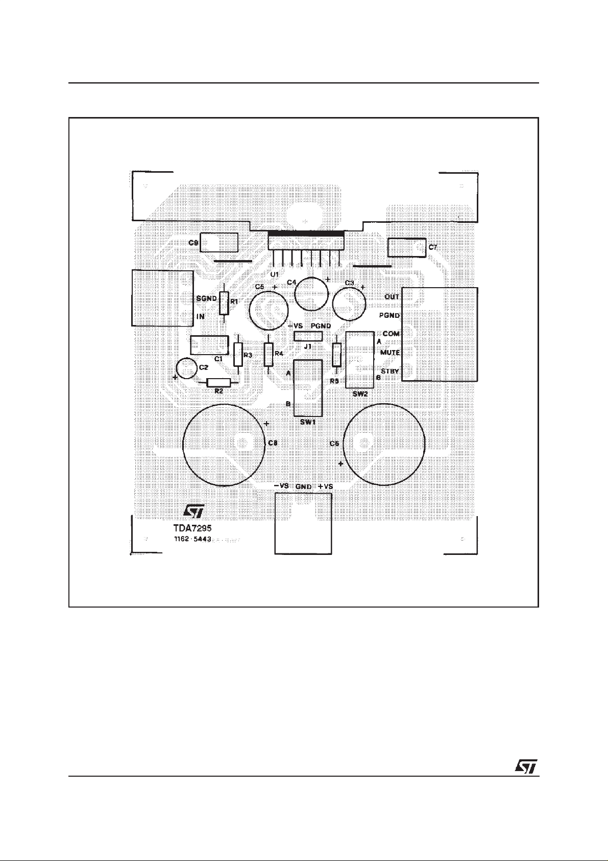
Figure 2:
P.C.B.and componentslayout of the circuit of figure 1. (1:1 scale)
Note:
The Stand-by andMute functions can be referred either to GND or -VS.
On the P.C.B. is possible to set both the configuration through the jumper J1.
4/13

TDA7295
APPLICATIONSUGGESTIONS(seeTest and Application Circuits of the Fig. 1)
The recommended values of the external components are those shown on the application circuit of Figure 1. Different values can be used;the following table can help the designer.
COMPONENTS SUGGESTED VALUE PURPOSE
R1 (*) 22k INPUT RESISTANCE INCREASE INPUT
R2 680
R3 (*) 22k INCREASE OF GAIN DECREASE OF GAIN
R4 22k ST-BY TIME
R5 10k MUTE TIME
C1 0.47µF INPUT DC
C2 22µF FEEDBACK DC
C3 10µF MUTE TIME
C4 10µF ST-BY TIME
Ω
CLOSED LOOP GAIN
SET TO 30dB (**)
CONSTANT
CONSTANT
DECOUPLING
DECOUPLING
CONSTANT
CONSTANT
LARGER THAN
SUGGESTED
IMPRDANCE
DECREASE OF GAIN INCREASE OF GAIN
LARGER ST-BY
ON/OFF TIME
LARGER MUTE
ON/OFF TIME
LARGER MUTE
ON/OFF TIME
LARGER ST-BY
ON/OFF TIME
SMALLER THAN
SUGGESTED
DECREASE INPUT
IMPEDANCE
SMALLER ST-BY
ON/OFF TIME;
POP NOISE
SMALLER MUTE
ON/OFF TIME
HIGHER LOW
FREQUENCY
CUTOFF
HIGHER LOW
FREQUENCY
CUTOFF
SMALLER MUTE
ON/OFF TIME
SMALLER ST-BY
ON/OFF TIME;
POP NOISE
C5 22µF BOOTSTRAPPING SIGNAL
C6, C8 1000µF SUPPLY VOLTAGE
C7, C9 0.1µF SUPPLY VOLTAGE
(*) R1 = R3 FOR POP OPTIMIZATION
(**) CLOSED LOOP GAINHAS TO BE≥24dB
BYPASS
BYPASS
DEGRADATION AT
LOW FREQUENCY
DANGER OF
OSCILLATION
DANGER OF
OSCILLATION
5/13

TDA7295
TYPICALCHARACTERISTICS
(ApplicationCircuit of fig 1 unlessotherwise specified)
Figure 3: OutputPower vs. Supply Voltage.
Figure 5: OutputPower vs. Supply Voltage
Figure4:
Distortionvs. Output Power
Figure6: Distortionvs. Output Power
Figure 7: Distortionvs. Frequency
6/13
Figure8: Distortionvs. Frequency

TYPICALCHARACTERISTICS (continued)
TDA7295
Figure 9:
Figure 11:
QuiescentCurrent vs. Supply Voltage
MuteAttenuationvs. V
pin10
Figure10:
SupplyVoltageRejectionvs.Frequency
Figure12: St-by Attenuation vs. V
pin9
Figure 13: Power Dissipationvs. OutputPower
Figure14:
PowerDissipation vs. Output Power
7/13

TDA7295
INTRODUCTION
In consumer electronics, an increasing demand
has arisen for very high power monolithic audio
amplifiers able to match,with a low cost the performance obtained from the best discrete designs.
The task of realizing this linear integrated circuit
in conventional bipolar technology is made extremely difficult by the occurence of 2nd breakdown phenomenon. It limits the safe operating
area (SOA) of the power devices, and as a consequence, the maximum attainableoutput power,
especiallyin presence of highly reactive loads.
Moreover, full exploitation of the SOA translates
into a substantial increase in circuit and layout
complexity due to the need for sophisticated protection circuits.
To overcome these substantial drawbacks, the
use of power MOS devices, which are immune
monic distortion and good behaviour over frequency response; moreover, an accurate control
of quiescent current is required.
A local linearizing feedback, provided by differential amplifier A, is used to fullfilthe above requirements, allowing a simple and effective quiescent
currentsetting.
Proper biasing of the power output transistors
alone is howevernot enoughto guarantee the absenceof crossover distortion.
While a linearization of the DC transfer characteristic of the stage is obtained, the dynamic behaviour of thesystem must be takeninto account.
A significant aid in keeping the distortion contributed by the final stage as low as possible is provided by the compensation scheme, which exploits the direct connection of the Miller capacitor
at the amplifier’s output to introduce a local AC
feedbackpath enclosing the output stage itself.
from secondarybreakdownis highly desirable.
The device described has therefore been devel-
oped in a mixed bipolar-MOS high voltage technology called BCD 100.
2) Protections
In designing a power IC, particular attention must
be reserved to the circuits devoted to protection
of the device from short circuit or overload condi-
1) OutputStage
The main design task one is confrontedwith while
developing an integrated circuit as a power operational amplifier, independently of the technology used, is that of realising the output stage.
The solution shown as a principle schematic by
Fig 15 represents the DMOS unity-gain output
buffer of the TDA7295.
This large-signal, high-power buffer must be capable of handling extremely high current and voltage levels while maintaining acceptably low har-
tions.
Due to the absence of the 2nd breakdown phe-
nomenon, the SOA of the power DMOS transis-
tors is delimited only by a maximum dissipation
curve dependent on the duration of the applied
stimulus.
In order to fully exploit the capabilities of the
power transistors, the protection scheme imple-
mented in this device combines a conventional
SOA protection circuit with a novel local tempera-
ture sensing technique which ” dynamically” con-
trols the maximumdissipation.
Figure 15: PrincipleSchematicof a DMOS unity-gain buffer.
8/13

Figure 16: Turn ON/OFF SuggestedSequence
+Vs
(V)
+35
-35
-Vs
VIN
(mV)
V
ST-BY
PIN #9
(V)
5V
TDA7295
V
MUTE
PIN #10
(V)
IP
(mA)
V
OUT
(V)
5V
OFF
ST-BY
PLAY
MUTE MUTE
In addition to the overload protection described
above, the device features a thermal shutdown
circuit which initially puts the device into a muting
state (@ Tj = 145
Figure 17:
SingleSignal ST-BY/MUTEControl
o
C) and then into stand-by (@
Circuit
MUTE STBY
MUTE/
ST-BY
20K
10K 30K
1N4148
10µF10µF
D93AU014
ST-BY OFF
D93AU013
o
Tj = 150
C).
Full protection against electrostatic discharges on
everypin isincluded.
3) OtherFeatures
The device is provided with both stand-by and
mute functions, independently driven by two
CMOSlogiccompatible input pins.
The circuits dedicated to the switching on and off
of the amplifier have been carefully optimized to
avoid any kindof uncontrolledaudible transient at
the output.
The sequence that we recommend during the
ON/OFFtransientsis shown by Figure 16.
The application of figure 17 shows the possibility
of using only one command for both st-by and
mute functions. On both the pins, the maximum
applicable range corresponds to the operating
supplyvoltage.
9/13

TDA7295
BRIDGE APPLICATION
Another application suggestion is the BRIDGE
configuration, where two TDA7295 are used, as
shown by the schematic diagram of figure25.
In this application, the value of the load must not
be lower than 8 Ohm for dissipation and current
capability reasons.
A suitable field of application includes HI-FI/TV
subwoofersrealisations.
The main advantagesoffered by this solution are:
Figure 18:
+Vs
BridgeApplicationCircuit
2200µF0.22µF
Vi
22K0.56µF
ST-BY/MUTE
20K
- High power performanceswith limitedsupply
voltagelevel.
- Considerablyhigh output power even with high
loadvalues (i.e. 16 Ohm).
The characteristics shown by figures 20 and 21,
measured with loads respectively 8 Ohm and 16
Ohm.
With Rl= 8 Ohm, Vs = ±22V the maximum output
power obtainable is 100W, while with Rl=16 Ohm,
Vs = ±30V the maximumPout is 100W.
137
3
1
4
10
+
-
9
6
22µF
14
2
815
22K
680
22µF
1N4148
10K 30K
0.56µF 22K
22µF
10
3
1
4
9
15 8
+
-
137
2200µF 0.22µF
6
22µF
14
2
22K
680
22K
-Vs
D93AU015A
10/13

TDA7295
Figure 19:
FrequencyResponseof the Bridge
Application
Figure 21: Distortionvs. OutputPower
Figure20: Distortion vs. Output Power
11/13

TDA7295
DIM.
Dia1 3.65 3.85 0.144 0.152
MIN. TYP. MAX. MIN. TYP. MAX.
A 5 0.197
B 2.65 0.104
C 1.6 0.063
D 1 0.039
E 0.49 0.55 0.019 0.022
F 0.66 0.75 0.026 0.030
G 1.02 1.27 1.52 0.040 0.050 0.060
G1 17.53 17.78 18.03 0.690 0.700 0.710
H1 19.6 0.772
H2 20.2 0.795
L 21.9 22.2 22.5 0.862 0.874 0.886
L1 21.7 22.1 22.5 0.854 0.870 0.886
L2 17.65 18.1 0.695 0.713
L3 17.25 17.5 17.75 0.679 0.689 0.699
L4 10.3 10.7 10.9 0.406 0.421 0.429
L7 2.65 2.9 0.104 0.114
M 4.25 4.55 4.85 0.167 0.179 0.191
M1 4.63 5.08 5.53 0.182 0.200 0.218
S 1.9 2.6 0.075 0.102
S1 1.9 2.6 0.075 0.102
mm inch
OUTLINE AND
MECHANICALDATA
Multiwatt15 V
12/13

TDA7295
Informationfurnishedisbelievedtobeaccurateandreliable.However,STMicroelectronicsassumesnoresponsibilityfortheconsequences
of useof suchinformationnor foranyinfringementof patentsor otherrights ofthirdpartieswhich may result from its use. No license is
grantedbyimplicationorotherwiseunderanypatentorpatentrightsof STMicroelectronics.Specificationmentionedinthispublicationare
subjecttochangewithoutnotice.Thispublicationsupersedesandreplacesallinformationpreviouslysupplied.STMicroelectronicsproducts
arenotauthorizedforuseascriticalcomponentsinlifesupportdevicesorsystemswithoutexpresswrittenapprovalofSTMicroelectronics.
Australia - Brazil - China - Finland - France - Germany - Hong Kong - India - Italy - Japan - Malaysia - Malta - Morocco -
TheSTlogoisaregisteredtrademarkofSTMicroelectronics
1999STMicroelectronics – Printed in Italy – AllRights Reserved
Singapore - Spain - Sweden - Switzerland - United Kingdom - U.S.A.
STMicroelectronics GROUP OF COMPANIES
http://www.st.com
13/13
 Loading...