


TDA7294
100V - 100W DMOS AUDIO AMPLIFIER WITH MUTE/ST-BY
VERY HIGH OPERATING VOLTAGE RANGE
(±40V)
DMOSPOWERSTAGE
HIGH OUTPUT POWER (UP TO 100W MU-
SIC POWER)
MUTING/STAND-BYFUNCTIONS
NOSWITCH ON/OFF NOISE
NOBOUCHEROTCELLS
VERYLOW DISTORTION
VERYLOW NOISE
SHORTCIRCUIT PROTECTION
THERMALSHUTDOWN
DESCRIPTION
The TDA7294 is a monolithic integrated circuit in
Multiwatt15 package, intended for use as audio
class AB amplifier in Hi-Fi field applications
(Home Stereo, self powered loudspeakers, Topclass TV). Thanks to the wide voltage range and
Figure1: TypicalApplication and TestCircuit
MULTIPOWERBCD TECHNOLOGY
Multiwatt15
ORDERING NUMBER: TDA7294V
to the high out current capability it is able to supply the highest power into both 4Ω and 8Ω loads
even in presence of poor supply regulation, with
high SupplyVoltage Rejection.
The built in muting function with turn on delay
simplifies the remoteoperation avoiding switching
on-off noises.
+VsC7 100nF C6 1000µF
VM
VSTBY
February 1996
R3 22K
C2
R2
22µF
680Ω
C1 470nF
R1 22K
R5 10K
R4 22K
C3 10µFC410µF
IN- 2
IN+
IN+MUTE
MUTE
STBY
3
4
10
9
TDA7294
MUTE
STBY
1
STBY-GND
+PWVs+Vs
713
-
+
THERMAL
SHUTDOWN
-Vs -PWVs
C9 100nF C8 1000µF
-Vs
S/C
PROTECTION
158
14
6
OUT
C5
22µF
BOOTSTRAP
D93AU011
1/16

TDA7294
PIN CONNECTION (Topview)
TAB connected to -V
BLOCKDIAGRAM
S
ABSOLUTE MAXIMUM RATINGS
Symbol Parameter Value Unit
V
I
O
P
tot
T
op
T
stg,Tj
2/16
Supply Voltage (No Signal) ±50 V
S
Output Peak Current 10 A
Power Dissipation T
=70°C50W
case
Operating Ambient Temperature Range 0 to 70 °C
Storage and Junction Temperature 150 °C

TDA7294
THERMALDATA
Symbol Description Value Unit
R
th j-case
ELECTRICALCHARACTERISTICS (Refer to the TestCircuit VS= ±35V, RL=8Ω,GV= 30dB;
=50Ω;T
R
g
Symbol Parameter Test Condition Min. Typ. Max. Unit
V
S
I
q
I
b
V
OS
I
OS
P
O
d Total Harmonic Distortion (**) P
SR Slew Rate 7 10 V/µs
G
V
G
V
e
N
f
L,fH
R
i
SVR Supply Voltage Rejection f = 100Hz; V
T
S
STAND-BY FUNCTION (Ref: -V
V
ST on
V
ST off
ATT
st-by
I
q st-by
MUTE FUNCTION (Ref: -V
V
Mon
V
Moff
ATT
mute
Note (*):
MUSIC POWER CONCEPT
MUSIC POWER is the maximal power which the amplifier is capable ofproducingacross the ratedload resistance (regardless of non linearity)
1 sec afterthe application of a sinusoidal input signalof frequency 1KHz.
Note (**): Tested with optimized Application Board (see fig. 2)
Note (***): Limited by themax. allowable current.
Thermal Resistance Junction-case Max 1.5 °C/W
=25°C,f = 1 kHz; unlessotherwisespecified.
amb
Supply Range ±10 ±40 V
Quiescent Current 20 30 60 mA
Input Bias Current 500 nA
Input OffsetVoltage +10 mV
Input OffsetCurrent +100 nA
RMS Continuous OutputPower d = 0.5%:
V
Music Power (RMS)
IEC268.3 RULES - ∆t = 1s (*)
= ± 35V, RL=8Ω
S
V
=±31V, RL=6Ω
S
V
=±27V, RL=4Ω
S
d = 10%
R
=8Ω ;VS=±38V
L
R
=6Ω ;VS=±33V
L
R
=4Ω ;VS=±29V (***)
L
= 5W; f = 1kHz
O
P
=0.1to50W;f=20Hzto20kHz
O
= ±27V, RL=4Ω:
V
S
P
= 5W; f = 1kHz
O
P
=0.1to50W;f=20Hzto20kHz
O
60
60
60
70
70
70
100
100
100
0.005
0.01
0.1
0.1
W
W
W
W
W
W
%
%
%
%
Open Loop Voltage Gain 80 dB
Closed Loop Voltage Gain 24 30 40 dB
Total Input Noise A = curve
f = 20Hz to 20kHz
1
25
µV
µV
Frequency Response (-3dB) PO= 1W 20Hz to 20kHz
Input Resistance 100 kΩ
= 0.5Vrms 60 75 dB
ripple
Thermal Shutdown 145 °C
or GND)
S
Stand-by on Threshold 1.5 V
Stand-by off Threshold 3.5 V
Stand-by Attenuation 70 90 dB
Quiescent Current @ Stand-by 1 3 mA
or GND)
S
Mute on Threshold 1.5 V
Mute off Threshold 3.5 V
Mute AttenuatIon 60 80 dB
3/16
TDA7294
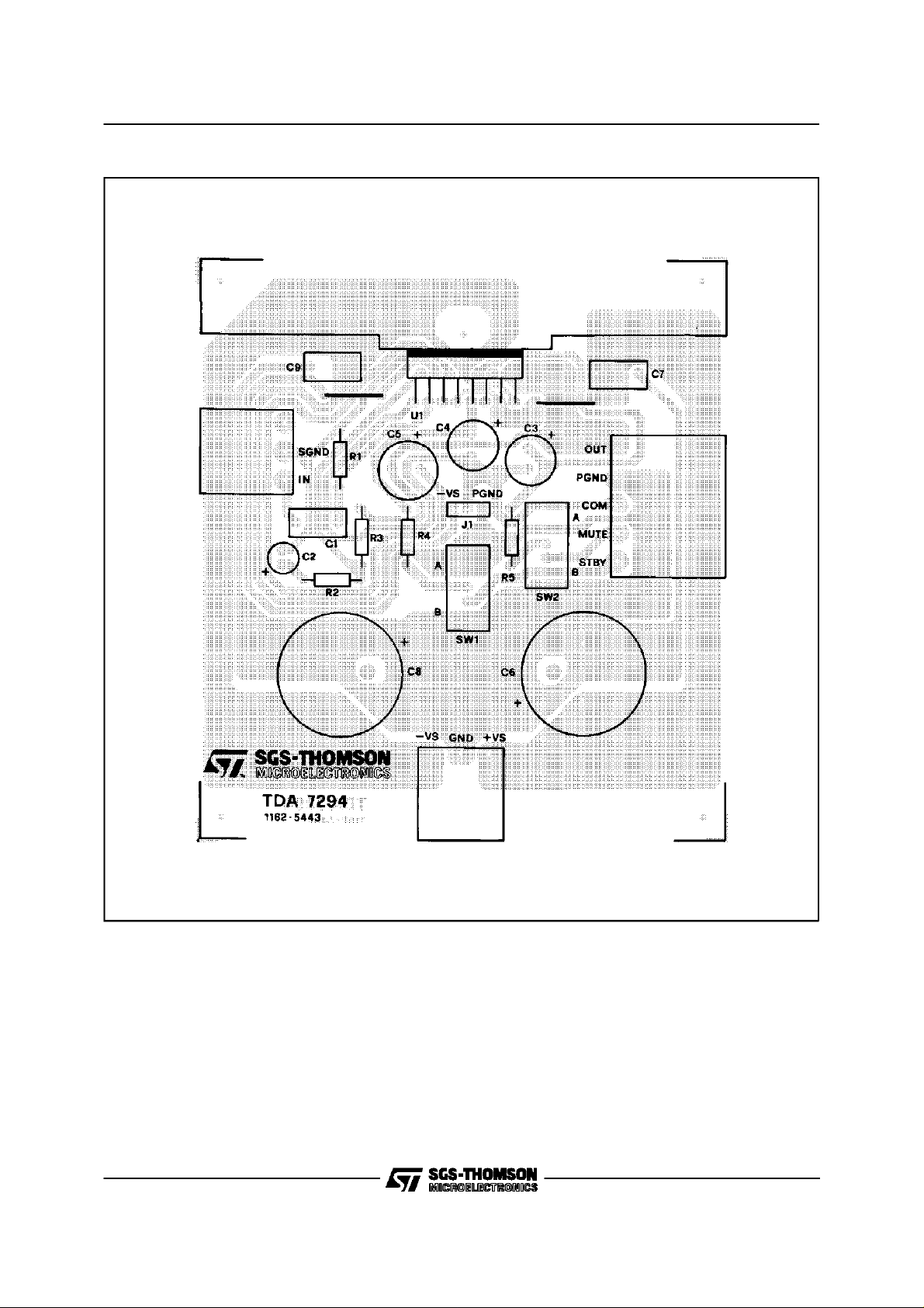
Figure2: P.C.B.and components layoutof the circuit of figure 1. (1:1 scale)
Note:
The Stand-by and Mute functions can be referred either to GND or -VS.
On the P.C.B. is possibleto set both the configuration through the jumper J1.
4/16

TDA7294
APPLICATION SUGGESTIONS(see Test and ApplicationCircuits of the Fig. 1)
The recommendedvalues of the external components are those shown on the applicationcircuit of Figure 1. Differentvaluescan be used;the followingtable can helpthe designer.
COMPONENTS SUGGESTED VALUE PURPOSE
R1 (*) 22k INPUT RESISTANCE INCREASE INPUT
R2 680Ω CLOSED LOOP GAIN
SET TO 30dB (**)
R3 (*) 22k INCREASE OF GAIN DECREASE OFGAIN
R4 22k ST-BY TIME
CONSTANT
R5 10k MUTE TIME
CONSTANT
C1 0.47µF INPUT DC
DECOUPLING
C2 22µF FEEDBACK DC
DECOUPLING
C3 10µF MUTE TIME
CONSTANT
C4 10µF ST-BY TIME
CONSTANT
LARGER THAN
SUGGESTED
IMPRDANCE
DECREASE OF GAIN INCREASE OF GAIN
LARGER ST-BY
ON/OFF TIME
LARGER MUTE
ON/OFF TIME
LARGER MUTE
ON/OFF TIME
LARGER ST-BY
ON/OFF TIME
SMALLER THAN
SUGGESTED
DECREASE INPUT
IMPEDANCE
SMALLER ST-BY
ON/OFF TIME;
POP NOISE
SMALLER MUTE
ON/OFF TIME
HIGHER LOW
FREQUENCY
CUTOFF
HIGHER LOW
FREQUENCY
CUTOFF
SMALLER MUTE
ON/OFF TIME
SMALLER ST-BY
ON/OFF TIME;
POP NOISE
C5 22µF BOOTSTRAPPING SIGNAL
C6, C8 1000µF SUPPLY VOLTAGE
C7, C9 0.1µF SUPPLY VOLTAGE
(*) R1 = R3 FOR POP OPTIMIZATION
(**) CLOSED LOOP GAINHAS TO BE ≥ 24dB
BYPASS
BYPASS
DEGRADATION AT
LOW FREQUENCY
DANGER OF
OSCILLATION
DANGER OF
OSCILLATION
5/16

TDA7294
TYPICALCHARACTERISTICS
(ApplicationCircuit of fig 1 unless otherwisespecified)
Figure3: OutputPower vs. SupplyVoltage.
Figure5: OutputPower vs. SupplyVoltage
Figure 4: Distortion vs. Output Power
Figure 6: Distortion vs. Output Power
Figure7: Distortionvs. Frequency
6/16
Figure 8: Distortion vs. Frequency

TYPICALCHARACTERISTICS (continued)
TDA7294
Figure9: QuiescentCurrentvs. Supply Voltage
Figure11: Mute Attenuationvs. V
pin10
Figure10:SupplyVoltage Rejectionvs.Frequency
Figure 12: St-byAttenuationvs. V
pin9
Figure13: PowerDissipationvs. OutputPower
Figure 14: PowerDissipation vs. OutputPower
7/16

TDA7294
INTRODUCTION
In consumer electronics, an increasing demand
has arisen for very high power monolithic audio
amplifiers able to match, with a low cost the performance obtained from the best discrete designs.
The task of realizing this linear integrated circuit
in conventional bipolar technology is made extremely difficult by the occurence of 2nd breakdown phenomenon. It limits the safe operating
area (SOA) of the power devices, and as a consequence, the maximum attainableoutput power,
especiallyin presence of highlyreactive loads.
Moreover, full exploitation of the SOA translates
into a substantial increase in circuit and layout
complexity due to the need for sophisticated protection circuits.
To overcome these substantial drawbacks, the
use of power MOS devices, which are immune
monic distortion and good behaviour over frequency response; moreover, an accurate control
of quiescentcurrent is required.
A local linearizing feedback, provided by differential amplifier A, is used to fullfil the above requirements, allowing a simple and effective quiescent
current setting.
Proper biasing of the power output transistors
alone is however not enough to guarantee the absence of crossoverdistortion.
While a linearization of the DC transfer characteristic of the stage is obtained, the dynamic behaviour of thesystemmust be taken into account.
A significant aid in keeping the distortion contributed by the final stage as low as possible is provided by the compensation scheme, which exploits the direct connection of the Miller capacitor
at the amplifier’s output to introduce a local AC
feedbackpath enclosing the output stage itself.
from secondary breakdown is highly desirable.
The device described has therefore been devel-
oped in a mixed bipolar-MOS high voltage technologycalled BCD100.
2) Protections
In designing a power IC, particular attention must
be reserved to the circuits devoted to protection
of the device from short circuit or overload condi-
1) Output Stage
Themain design taskone is confrontedwith while
developing an integrated circuit as a power operational amplifier, independently of the technologyused, is that of realizing theoutput stage.
Thesolution shown as a principleshematicby Fig
15 represents the DMOS unity-gain output buffer
of the TDA7294.
This large-signal, high-power buffer must be capable of handling extremely high current and voltage levels while maintaining acceptably low har-
tions.
Due to the absence of the 2nd breakdown phe-
nomenon, the SOA of the power DMOS transis-
tors is delimited only by a maximum dissipation
curve dependent on the duration of the applied
stimulus.
In order to fully exploit the capabilities of the
power transistors, the protection scheme imple-
mented in this device combines a conventional
SOA protection circuit with a novel local tempera-
ture sensing technique which ” dynamically” con-
trols the maximum dissipation.
Figure15: PrincipleSchematicof a DMOSunity-gain buffer.
8/16

Figure16: Turn ON/OFF SuggestedSequence
+Vs
(V)
+35
-35
-Vs
VIN
(mV)
V
ST-BY
PIN #9
(V)
5V
TDA7294
V
MUTE
PIN #10
(V)
IP
(mA)
V
OUT
(V)
5V
OFF
ST-BY
PLAY
MUTE MUTE
In addition to the overload protection described
above, the device features a thermal shutdown
circuitwhich initially puts the device into a muting
state (@ Tj = 145
o
C) and then into stand-by (@
Figure17: SingleSignal ST-BY/MUTEControl
Circuit
MUTE STBY
MUTE/
ST-BY
20K
10K 30K
1N4148
10µF10µF
D93AU014
ST-BY OFF
D93AU013
o
Tj =150
C).
Full protection against electrostatic discharges on
every pin is included.
3) Other Features
The device is provided with both stand-by and
mute functions, independently driven by two
CMOSlogic compatibleinput pins.
The circuits dedicated to the switchingon and off
of the amplifier have been carefully optimized to
avoid any kind of uncontrolled audible transient at
the output.
The sequence that we recommend during the
ON/OFF transients is shown by Figure 16.
The application of figure 17 shows the possibility
of using only one command for both st-by and
mute functions. On both the pins, the maximum
applicable range corresponds to the operating
supply voltage.
9/16

TDA7294
APPLICATION INFORMATION
HIGH-EFFICIENCY
Constraints of implementing high power solutions
are the power dissipation and the size of the
power supply. These are both due to the low efficiency of conventional AB class amplifier approaches.
Here below (figure 18) is described a circuit proposal for a high efficiency amplifier which can be
adopted for both HI-FI and CAR-RADIO applications.
The TDA7294 is a monolithic MOS power amplifier which can be operated at 80V supply voltage
(100V with no signal applied) while delivering output currents up to ±10 A.
This allows the use of this device as a very high
power amplifier (up to 180W as peak power with
T.H.D.=10 % and Rl = 4 Ohm);the only drawback
is the power dissipation, hardly manageable in
the above power range.
Figure 20 shows the power dissipation versus
output power curve for a class AB amplifier, comparedwith a high efficiencyone.
In orderto dimension the heatsink (and the power
supply), a generally used average output power
value is one tenth of the maximum output power
at T.H.D.=10 %.
From fig. 20, where the maximum power is
around 200 W,we get an average of 20 W, in this
condition, for a class AB amplifier the average
power dissipation is equalto 65 W.
The typical junction-to-case thermal resistance of
the TDA7294 is 1
avoid that, in worst caseconditions, the chip tem-
perature exceedes 150
of the heatsink must be 0.038
bient temperatureof 50
o
C/W (max= 1.5oC/W). To
o
C, the thermal resistance
o
o
C).
C/W (@ max am-
As the above value is pratically unreachable; a
high efficiency system is needed in those cases
where the continuousRMS output poweris higher
than 50-60 W.
The TDA7294 was designed to work also in
higher efficiency way.
For this reason there are four power supply pins:
two intended for the signal part and two for the
power part.
T1 and T2 are two power transistors that only op-
erate when the output power reaches a certain
threshold (e.g. 20 W). If the output power in-
creases, these transistors are switched on during
the portion of the signal where more output volt-
age swing is needed, thus ”bootstrapping” the
power supplypins (#13 and #15).
The current generators formed by T4, T7, zener
Figure18: High Efficiency ApplicationCircuit
+40V
+20V
C9
C7
100nF
C8
100nF
330nF
C10
330nF
R1
R2
2
PLAY
ST-BY
2
1N4148
GND
-20V
-40V
C1
1000µF
C2
1000µF
C3
100nF
C4
100nF
C5
1000µF
C6
1000µF
IN
D5
D1 BYW98100
C11 330nF
R16
13K
C13 10µF
R13 20K
R14 30K
R15 10K
C14
10µF
D2 BYW98100
3
4
TDA7294
9
815
10
T3
BC394
T1
BDX53A
270
L1 1µH
137
14
L2 1µH
2
6
1
270
T2
BDX54A
D3 1N4148
R3 680
R16
13K
C15
22µF
D4 1N4148
T6
BC393
C11 22µF
L3 5µH
270
R4
270
T4
BC393
Z1 3.9V
Z2 3.9V
T7
BC394
R9
270
R7
3.3K
R8
3.3K
D93AU016
R5
270
R6
20K
R10
270
T5
BC393
C16
1.8nF
OUT
C17
1.8nF
T8
BC394
R11
29K
10/16

Figure19: P.C.B.and ComponentsLayout of the Circuit of figure 18 (1:1 scale)
TDA7294
diodesZ1,Z2 and resistorsR7,R8 define the minimum drop across the power MOS transistors of
the TDA7294. L1, L2, L3 and the snubbers C9,
R1 and C10, R2 stabilize the loops formed by the
”bootstrap” circuits and the output stage of the
TDA7294.
In figures 21,22 the performances of the system
in terms of distortion and output power at various
frequencies (measured on PCB shown in fig. 19)
are displayed.
The outputpower that the TDA7294 in highefficiency application is able to supply at
Vs = +40V/+20V/-20V/-40V; f =1 KHz is:
-Pout = 150 W @ T.H.D.=10 % with Rl= 4 Ohm
- Pout = 120 W @ ” = 1% ” ” ”
- Pout = 100 W @ ” =10% with Rl= 8 Ohm
- Pout = 80 W @ ” = 1% ” ” ”
Results from efficiency measurements (4 and 8
Ohm loads, Vs = ±40V) are shown by figures 23
and 24. We have 3 curves: total power dissipa-
tion, power dissipation of the TDA7294 and
power dissipation of the darlingtons.
By considering again a maximum average
output power (music signal) of 20W, in case
of the high efficiency application, the thermal
resistance value needed from the heatsink is
o
C/W (Vs =±40 V and Rl= 4 Ohm).
2.2
All components (TDA7294 and power transistors
T1 and T2) can be placed on a 1.5
o
C/W heatsink,
with the power darlingtons electrically insulated
from the heatsink.
Since the total power dissipation is less than that
of a usual class AB amplifier, additional cost savings can be obtained while optimizing the power
supply, even with a high headroom.
11/16

TDA7294
Figure20: PowerDissipationvs. OutputPower
HIGH-EFFICIENCY
Figure22: Distortionvs. Output Power
Figure 21: Distortionvs. Output Power
Figure 23: PowerDissipation vs. OutputPower
Figure24: PowerDissipationvs. OutputPower
12/16

TDA7294
BRIDGEAPPLICATION
Another application suggestion is the BRIDGE
configuration, where two TDA7294 are used, as
shownby the schematicdiagram of figure 25.
In this application, the value of the load must not
be lower than 8 Ohm for dissipation and current
capability reasons.
A suitable field of application includes HI-FI/TV
subwoofersrealizations.
Themain advantagesoffered by this solutionare:
Figure25: BridgeApplicationCircuit
+Vs
2200µF0.22µF
Vi
22K0.56µF
ST-BY/MUTE
20K
3
1
4
10
- High powerperformanceswith limited supply
voltagelevel.
- Considerablyhigh output power even with high
load values(i.e. 16 Ohm).
The characteristics shown by figures 27 and 28,
measured with loads respectively 8 Ohm and 16
Ohm.
With Rl= 8 Ohm, Vs = ±25V the maximumoutput
power obtainable is 150 W, while with Rl=16
Ohm, Vs = ±35V the maximum Pout is 170 W.
137
6
22µF
+
-
TDA7294
9
14
2
815
22K
680
22µF
1N4148
10K 30K
0.56µF 22K
22µF
9
10
TDA7294
3
1
4
15 8
+
-
137
2200µF 0.22µF
6
22µF
14
2
22K
680
22K
-Vs
D93AU015A
13/16

TDA7294
Figure26: FrequencyResponse of the Bridge
Application
Figure28: Distortionvs. Output Power
Figure 27: Distortionvs. Output Power
14/16

MULTIWATT15 PACKAGE MECHANICAL DATA (Vertical)
TDA7294
DIM.
MIN. TYP. MAX. MIN. TYP. MAX.
A 5 0.197
B 2.65 0.104
C 1.6 0.063
D 1 0.039
E 0.49 0.55 0.019 0.022
F 0.66 0.75 0.026 0.030
G 1.14 1.27 1.4 0.045 0.050 0.055
G1 17.57 17.78 17.91 0.692 0.700 0.705
H1 19.6 0.772
H2 20.2 0.795
L 22.1 22.6 0.870 0.890
L1 22 22.5 0.866 0.886
L2 17.65 18.1 0.695 0.713
L3 17.25 17.5 17.75 0.679 0.689 0.699
L4 10.3 10.7 10.9 0.406 0.421 0.429
L7 2.65 2.9 0.104 0.114
M 4.2 4.3 4.6 0.165 0.169 0.181
M1 4.5 5.08 5.3 0.177 0.200 0.209
S 1.9 2.6 0.075 0.102
S1 1.9 2.6 0.075 0.102
Dia1 3.65 3.85 0.144 0.152
mm inch
15/16

TDA7294
Information furnished is believed to be accurate and reliable. However, SGS-THOMSON Microelectronics assumes no responsibility for the
consequences of use of such information nor for any infringement of patents or other rights of third parties which may result fromits use. No
license is granted by implication or otherwise under any patent or patent rights of SGS-THOMSON Microelectronics. Specifications mentioned in this publication are subject to change without notice. This publication supersedes and replaces all information previously supplied.
SGS-THOMSON Microelectronics products are not authorized for use as critical components in lifesupport devices or systems without express written approval of SGS-THOMSON Microelectronics.
1996 SGS-THOMSON Microelectronics AllRights Reserved
Australia - Brazil-France - Germany - Hong Kong - Italy - Japan - Korea - Malaysia - Malta - Morocco -The Netherlands -Singapore -
SGS-THOMSON Microelectronics GROUP OF COMPANIES
Spain - Sweden - Switzerland - Taiwan - Thaliand - United Kingdom - U.S.A.
16/16
 Loading...