

TDA7293
120V - 100W DMOS AUDIO AMPLIFIER WITHMUTE/ST-BY
VERY HIGH OPERATING VOLTAGE RANGE
(±50V)
DMOSPOWERSTAGE
HIGH OUTPUT POWER (100W @ THD =
10%, R
L =8
,VS=±40V)
Ω
MUTING/STAND-BYFUNCTIONS
NO SWITCHON/OFF NOISE
VERYLOW DISTORTION
VERYLOW NOISE
SHORTCIRCUIT PROTECTION
THERMALSHUTDOWN
CLIPDETECTOR
MODULARITY (MORE DEVICES CAN BE
EASILY CONNECTED IN PARALLEL TO
DRIVE VERYLOW IMPEDANCES)
DESCRIPTION
The TDA7293 is a monolithic integrated circuit in
Multiwatt15 package, intended for use as audio
class AB amplifier in Hi-Fi field applications
(Home Stereo, self powered loudspeakers, Top-
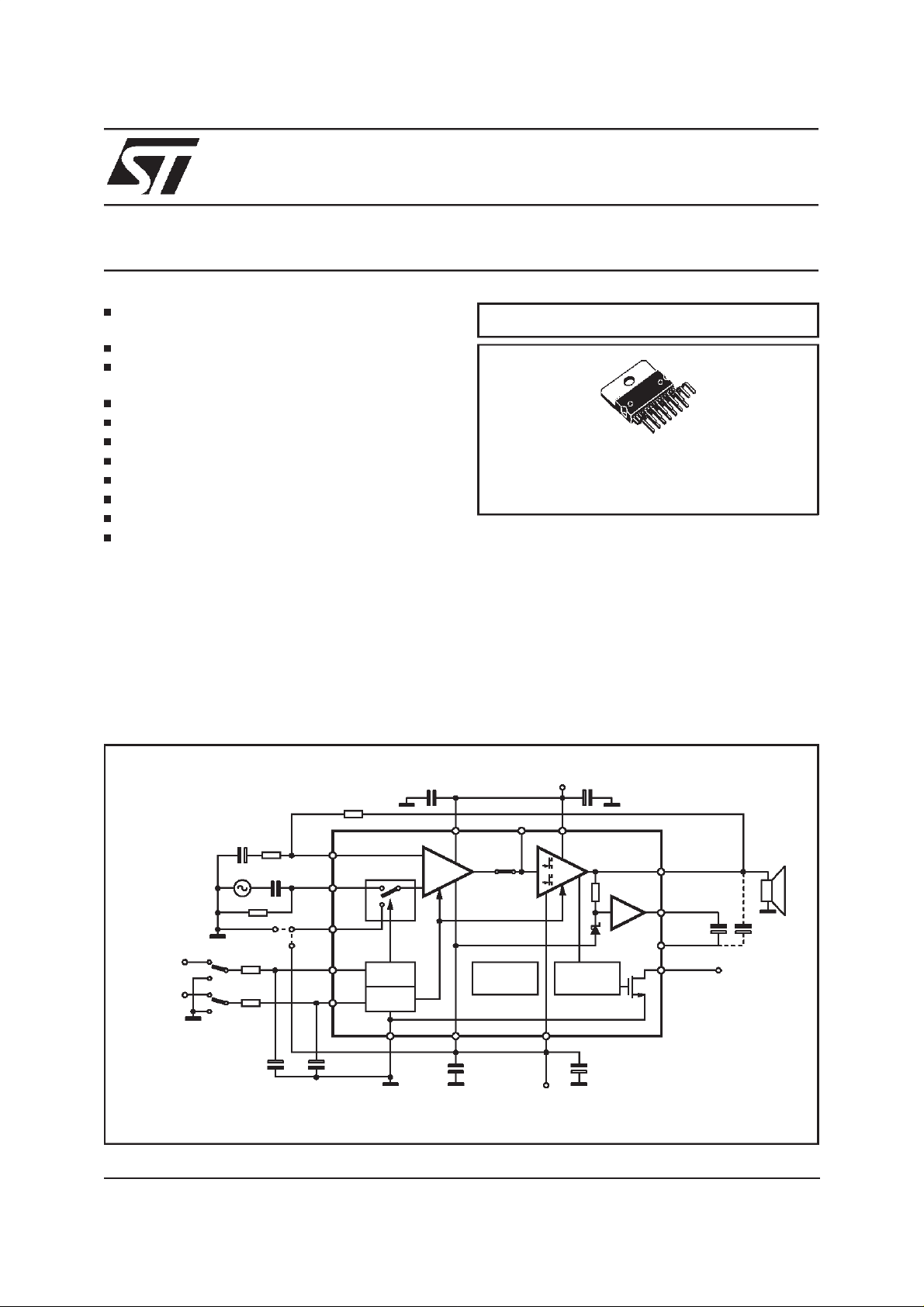
Figure 1: Typical Applicationand Test Circuit
MULTIPOWER BCD TECHNOLOGY
Multiwatt15
ORDERING NUMBER: TDA7293V
class TV). Thanks to the wide voltage range and
to the high out current capability it is able to supply the highest powerinto both4Ω and 8Ω loads.
The built in muting function with turn on delay
simplifiesthe remote operation avoiding switching
on-off noises.
Parallel mode is made possible by connecting
more device through of pin11. High output power
can be deliveredto verylow impedance loads, so
optimizingthe thermal dissipation ofthe system.
VMUTE
VSTBY
December1999
C7 100nF C6 1000µF
R3 22K
C2
R2
22µF
680Ω
C1 470nF
R1 22K
R5 10K
R4 22K
C3 10µFC410µF
IN- 2
IN+
3
4
SGND
(**)
10
MUTE
9
STBY
(*) see Application
(**) for SLAVE function
note
MUTE
STBY
1
STBY-GND
+Vs
BUFFER DRIVER
713
11
-
+
THERMAL
SHUTDOWN
-Vs -PWVs
C9 100nF C8 1000µF
PROTECTION
158
-Vs
+PWVs+Vs
S/C
14
12
6
5
D97AU805A
OUT
BOOT
LOADER
C5
22µF
BOOTSTRAP
CLIP DET
(*)
VCLIP
1/13
TDA7293
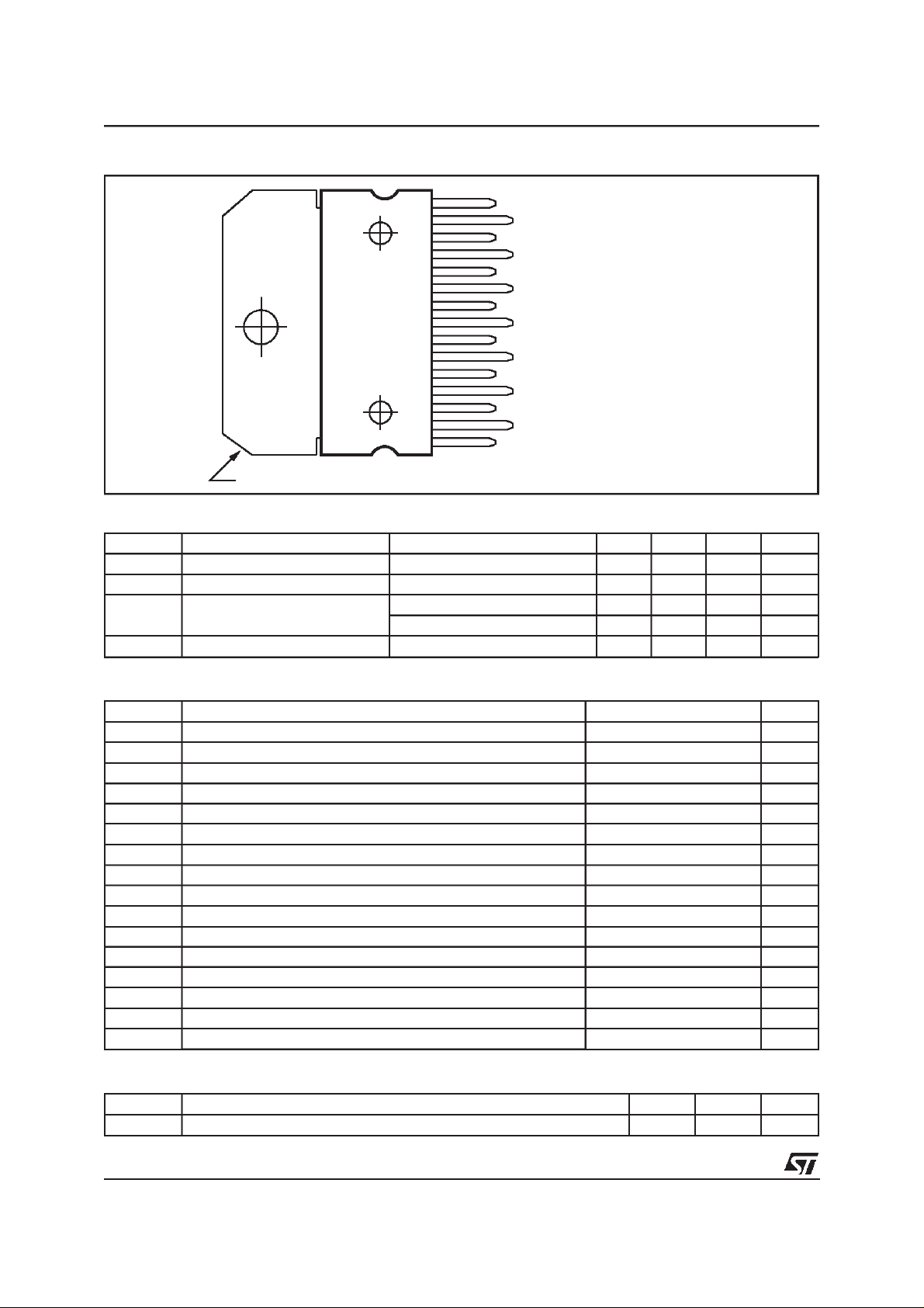
PIN CONNECTION (Top view)
TAB CONNECTED TO PIN 8
15
14
13
12
11
10
9
8
7
6
5
4
3
2
1
D97AU806
-VS(POWER)
OUT
(POWER)
+V
S
BOOTSTRAP LOADER
BUFFER DRIVER
MUTE
STAND-BY
-V
(SIGNAL)
S
+VS(SIGNAL)
BOOTSTRAP
CLIP AND SHORT CIRCUIT DETECTOR
SIGNAL GROUND
NON INVERTING INPUT
INVERTING INPUT
STAND-BY GND
QUICK REFERENCEDATA
Symbol Parameter Test Conditions Min. Typ. Max. Unit
V
S
G
LOOP
P
tot
SVR Supply Voltage Rejection 75 dB
Supply Voltage Operating ±12 æ 50 V
Closed Loop Gain 26 40 dB
Output Power VS=±45V; RL=8Ω; THD = 10% 140 W
= ±30V; RL =4Ω; THD = 10% 110 W
V
S
ABSOLUTE MAXIMUM RATINGS
Symbol Parameter Value Unit
V
S
V
V
2 -V3 Maximum Differential Inputs ±30 V
V
V
V
V
V
V
V
10
11 Buffer Voltage Referred to -VS 120 V
V
V
12
I
O
P
tot
T
op
T
stg,Tj
Supply Voltage (No Signal)
V
1
2
3
4
5 Clip Detector Voltage Referred to -VS 120 V
6
9
STAND-BY
Input Voltage (inverting) Referred to -V
Input Voltage (non inverting) Referred to -V
Signal GND Voltage Referred to -V
Bootstrap Voltage Referred to -V
Stand-by Voltage Referred to -V
Mute Voltage Referred to -V
Bootstrap Loader Voltage Referred to -V
GND Voltage Referred to -VS(pin 8) 90 V
S
S
S
S
S
S
S
Output Peak Current 10 A
Power Dissipation T
=70°C50W
case
Operating Ambient Temperature Range 0 to 70
Storage and Junction Temperature 150
60 V
±
90 V
90 V
90 V
120 V
120 V
120 V
100 V
THERMAL DATA
Symbol Description Typ Max Unit
R
th j-case
Thermal Resistance Junction-case 1 1.5
°
°
C/W
°
C
C
2/13
TDA7293
ELECTRICALCHARACTERISTICS(Refer to the Test Circuit VS= ±40V,RL=8Ω,Rg=50Ω;
T
=25°C,f = 1 kHz; unlessotherwise specified).
amb
Symbol Parameter Test Condition Min. Typ. Max. Unit
V
V
I
P
Supply Range
S
Quiescent Current 30 mA
I
q
Input Bias Current 0.3 1
I
b
Input Offset Voltage -10 10 mV
OS
Input Offset Current 0.2
OS
RMS Continuous Output Power d = 1%:
O
R
=4Ω; VS = ± 29V,
L
d = 10%
R
=4Ω ;VS=±29V
L
d Total Harmonic Distortion (**) P
I
Current Limiter Threshold 6.5 A
SC
= 5W; f = 1kHz
O
P
=0.1to 50W;f = 20Hz to 15kHz
O
SR Slew Rate 15 V/µs
G
G
e
Open Loop Voltage Gain 80 dB
V
Closed Loop Voltage Gain (1) 30 dB
V
Total Input Noise A = curve
N
f = 20Hz to 20kHz
R
SVR Supply Voltage Rejection f = 100Hz; V
T
Input Resistance 100 kΩ
i
= 0.5Vrms 75 dB
ripple
Thermal Protection DEVICE MUTED 150
S
DEVICE SHUT DOWN 160 °C
STAND-BY FUNCTION (Ref: to pin 1)
V
V
ATT
I
q st-by
ST on
ST off
Stand-by on Threshold 1.5 V
Stand-by off Threshold 3.5 V
Stand-by Attenuation 70 90 dB
st-by
Quiescent Current @ Stand-by 0.5 mA
MUTE FUNCTION (Ref: to pin 1)
V
V
ATT
Mute on Threshold 1.5 V
Mon
Mute off Threshold 3.5 V
Moff
Mute AttenuatIon 60 80 dB
mute
CLIP DETECTOR
Ω
Duty Duty Cycle ( pin 5) THD = 1% ; RL = 10K
to 5V 10 %
THD = 10% ;
RL = 10KΩto 5V
I
CLEAK
SLAVE FUNCTION pin 4 (Ref: to pin 8 -V
V
Slave
V
Master
Note (1): GVmin ≥ 26dB
Note: Pin 11 only for modular connection.Max external load 1MΩ/10 pF,only for test purpose
Note (**): Tested with optimized Application Board (see fig. 2)
SlaveThreshold 1V
Master Threshold 3 V
PO = 50W 1 µA
)
S
12
±
50 V
±
80
80
100
100
0.005
0.1
1
25
40 %
A
µ
A
µ
W
W
%
%
V
µ
V
µ
C
°
3/13
TDA7293
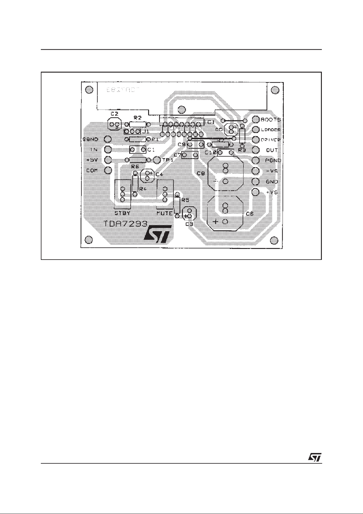
Figure 2: Typical Application P.C. Boardand ComponentLayout (scale1:1)
4/13

TDA7293
APPLICATIONSUGGESTIONS(seeTest andApplication Circuitsof the Fig. 1)
The recommendedvalues of the external components are those shown on the application circuit of Figure 1. Different valuescan be used; the followingtable can help the designer.
COMPONENTS SUGGESTED VALUE PURPOSE
LARGER THAN
SUGGESTED
R1 (*) 22k INPUT RESISTANCE INCREASE INPUT
IMPEDANCE
R2 680
Ω
CLOSED LOOP GAIN
DECREASE OF GAIN INCREASE OF GAIN
SMALLER THAN
SUGGESTED
DECREASE INPUT
IMPEDANCE
SET TO 30dB (**)
R3 (*) 22k INCREASE OF GAIN DECREASE OF GAIN
R4 22k ST-BY TIME
CONSTANT
LARGER ST-BY
ON/OFF TIME
SMALLER ST-BY
ON/OFF TIME;
POP NOISE
R5 10k MUTE TIME
CONSTANT
C1 0.47µF INPUT DC
DECOUPLING
LARGER MUTE
ON/OFF TIME
SMALLER MUTE
ON/OFF TIME
HIGHER LOW
FREQUENCY
CUTOFF
C2 22µF FEEDBACK DC
DECOUPLING
HIGHER LOW
FREQUENCY
CUTOFF
C3 10µF MUTE TIME
CONSTANT
C4 10µF ST-BY TIME
CONSTANT
LARGER MUTE
ON/OFF TIME
LARGER ST-BY
ON/OFF TIME
SMALLER MUTE
ON/OFF TIME
SMALLER ST-BY
ON/OFF TIME;
POP NOISE
C5 22µFXN (***) BOOTSTRAPPING SIGNAL
C6, C8 1000µF SUPPLY VOLTAGE
C7, C9 0.1µF SUPPLY VOLTAGE
(*) R1 = R3 for pop optimization
(**) Closed Loop Gain has to be≥26dB
(***) Multiplay this value for thenumber of modular part connected
Slave function:pin 4 (Ref to pin8 -VS)
+3V
-V
S
+1V
-V
S
-V
S
MASTER
UNDEFINED
SLAVE
D98AU821
DEGRADATION AT
LOW FREQUENCY
BYPASS
DANGER OF
BYPASS
OSCILLATION
Note:
If in the application, the speakers are connected
via long wires, it is a good rule to add between
the output and GND, a BoucherotCell, in order to
avoid dangerous spurious oscillations when the
speakersterminal are shorted.
The suggested Boucherot Resistor is 3.9Ω/2W
and the capacitoris 1µF.
5/13

TDA7293
INTRODUCTION
In consumer electronics, an increasing demand
has arisen for very high power monolithic audio
amplifiers able to match, with a low cost, the performance obtained from the best discrete designs.
The task of realizing this linear integrated circuit
in conventional bipolar technology is made extremely difficult by the occurence of 2nd breakdown phoenomenon. It limits the safe operating
area (SOA) of the power devices, and, as a consequence, the maximum attainable output power,
especiallyin presenceof highlyreactive loads.
Moreover, full exploitation of the SOA translates
into a substantial increase in circuit and layout
complexity due to the need of sophisticated protection circuits.
To overcome these substantial drawbacks, the
use of power MOS devices, which are immune
from secondarybreakdown is highly desirable.
The device described has therefore been developed in a mixed bipolar-MOS high voltage technology called BCDII100/120.
1) Output Stage
The main design task in developpinga power operational amplifier, independently of the technology used, is that of realization of the output stage.
The solution shown as a principle shematic by
Fig3 represents the DMOS unity - gain output
buffer of the TDA7293.
This large-signal, high-power buffer must be capable of handling extremely high current and voltage levels while maintaining acceptably low harmonic distortion and good behaviour over
frequency response; moreover, an accurate control of quiescentcurrent is required.
A local linearizing feedback, provided by differential amplifier A, is used to fullfilthe above requirements, allowing a simple and effective quiescent
currentsetting.
Proper biasing of the power output transistors
alone is howevernot enough to guarantee the absenceof crossoverdistortion.
While a linearization of the DC transfer characteristic of the stage is obtained, the dynamic behaviour of the systemmust be taken into account.
A significant aid in keeping the distortion contributed by the final stage as low as possible is provided by the compensation scheme, which exploits the direct connection of the Miller capacitor
at the amplifier’s output to introduce a local AC
feedbackpath enclosing the outputstage itself.
2) Protections
In designing a power IC, particular attention must
be reserved to the circuits devoted to protection
of the device from short circuit or overload conditions.
Due to the absence of the 2nd breakdown phenomenon, the SOA of the power DMOS transistors is delimited only by a maximum dissipation
curve dependent on the duration of the applied
stimulus.
In order to fully exploit the capabilities of the
power transistors, the protection scheme implemented in this device combines a conventional
SOA protection circuit with a novellocal temperature sensing technique which ” dynamically” controls the maximumdissipation.
Figure 3: PrincipleSchematic of a DMOSunity-gainbuffer.
6/13

Figure 4: Turn ON/OFFSuggestedSequence
+Vs
(V)
+40
-40
-Vs
VIN
(mV)
V
ST-BY
PIN #9
(V)
5V
TDA7293
V
MUTE
PIN #10
(V)
IQ
(mA)
V
OUT
(V)
5V
OFF
ST-BY
PLAY
MUTE MUTE
In addition to the overload protection described
above, the device features a thermal shutdown
circuit which initially puts the device into a muting
state (@ Tj = 150
Tj = 160
o
C).
o
C) and then into stand-by (@
Full protectionagainst electrostaticdischarges on
every pin is included.
Figure 5:
SingleSignal ST-BY/MUTEControl
Circuit
MUTE STBY
MUTE/
ST-BY
20K
10K 30K
1N4148
10µF10µF
D93AU014
3) OtherFeatures
The device is provided with both stand-by and
ST-BY OFF
D98AU817
mute functions, independently driven by two
CMOSlogic compatible input pins.
The circuits dedicated to the switching on and off
of the amplifier have been carefully optimized to
avoid any kindof uncontrolledaudible transient at
the output.
The sequence that we recommend during the
ON/OFFtransientsis shown by Figure 4.
The application of figure 5 shows thepossibility of
using only one command for both st-by and mute
functions. On both the pins, the maximum applicable range corresponds to the operating supply
voltage.
APPLICATION INFORMATION
HIGH-EFFICIENCY
Constraints of implementinghigh power solutions
are the power dissipation and the size of the
power supply. These are both due to the low efficiency of conventional AB class amplifier approaches.
Here below (figure 6) is described a circuit proposal for a high efficiency amplifier which can be
adopted for both HI-FI and CAR-RADIO applications.
7/13

TDA7293
The TDA7293 is a monolithic MOS power amplifier which can be operated at 100V supplyvoltage
(120V with no signal applied) while delivering output currentsup to ±6.5 A.
This allows the use of this device as a very high
power amplifier (up to 180W as peak power with
T.H.D.=10 % and Rl = 4 Ohm);the only drawback
is the power dissipation, hardly manageable in
the above power range.
The typical junction-to-case thermal resistance of
the TDA7293 is 1
avoid that, in worst case conditions, the chip temperature exceedes150
of the heatsink must be 0.038
bient temperatureof 50
o
C/W (max= 1.5oC/W). To
o
C, the thermal resistance
o
o
C).
C/W (@ max am-
As the above value is pratically unreachable; a
high efficiency system is needed in those cases
where the continuousRMS output power is higher
than 50-60 W.
The TDA7293 was designed to work also in
higher efficiencyway.
For this reason there are four power supply pins:
two intended for the signal part and two for the
power part.
T1 and T2 are two power transistors that only
operate when the output power reaches a certain
threshold (e.g. 20 W). If the output power increases, these transistors are switched on during
the portion of the signal where more output voltage swing is needed, thus ”bootstrapping” the
power supply pins(#13 and #15).
The current generators formed by T4, T7, zener
diodes Z1, Z2 and resistors R7,R8 define the
minimum drop across the power MOS transistors
of the TDA7293. L1, L2, L3 and the snubbersC9,
R1 and C10, R2 stabilize the loops formed by the
”bootstrap” circuits and the output stage of the
TDA7293.
By considering again a maximum average
output power (music signal) of 20W, in case
of the high efficiency application, the thermal
resistance value needed from the heatsink is
o
C/W (Vs =±50 V and Rl= 8 Ohm).
2.2
All components (TDA7293 and power transistors T1 and T2) can be placed on a 1.5
o
C/W
heatsink, with the power darlingtons electrically
insulatedfrom the heatsink.
Since the total power dissipation is less than that
of a usual class AB amplifier, additional cost savings can be obtained while optimizing the power
supply, even witha high heatsink.
BRIDGE APPLICATION
Another application suggestion is the BRIDGE
configuration,where two TDA7293 are used.
In this application, the value of the load must not
be lower than 8 Ohm for dissipation and current
capability reasons.
A suitable field of application includes HI-FI/TV
subwoofersrealizations.
The main advantagesoffered by this solutionare:
- High power performanceswith limited supply
voltagelevel.
- Considerablyhigh output power even with high
loadvalues (i.e. 16 Ohm).
With Rl= 8 Ohm, Vs = ±25V the maximum output
power obtainable is 150 W, while with Rl=16
Ohm,Vs = ±40V the maximumPout is 200W.
APPLICATION NOTE: (ref. fig. 7)
ModularApplication (moreDevices in Parallel)
The use of the modular application lets very high
power be delivered to very low impedance loads.
The modular application implies one device to act
as a master and the others as slaves.
The slave power stages are driven by the master
device and work in parallel all together, while the
input and the gain stages of the slave device are
disabled, the figure below shows the connections
required to configure two devices to work together.
The master chip connections are the same as
the normal single ones.
The outputs can be connected together with-
out the need of any ballast resistance.
The slave SGND pin must be tied to the negative supply.
The slave ST-BY pin must be connected to
ST-BYpin.
The bootstrap lines must be connected together and the bootstrap capacitor must be increased: for N devices the boostrap capacitor
must be 22µF times N.
The slave Mute and IN-pinsmust be grounded.
THE BOOTSTRAP CAPACITOR
For compatibility purpose with the previous devices of the family, the boostrap capacitor can be
connectedboth between the bootstrappin (6) and
the output pin (14) or between the boostrap pin
(6) and the bootstraploader pin (12).
When the bootcap is connected between pin 6
and 14, the maximum supply voltage in presence
of output signal is limited to 100V, due the bootstrapcapacitor overvoltage.
When the bootcap is connected between pins 6
and 12 the maximum supply voltageextend to the
full voltagethat thetechnologycan stand:120V.
This is accomplished by the clamp introduced at
the bootstrap loader pin (12): this pin follows the
output voltage up to 100V and remains clamped
at 100V for higher output voltages. This feature
lets the output voltage swing up to a gate-source
voltagefrom the positive supply (V
S -3 to 6V)
8/13

Figure 6: High EfficiencyApplication Circuit
TDA7293
+50V
D6
1N4001
PLAY
ST-BY
D5
1N4148
D1 BYW98100
C12 330nF
IN
C13 10µF
R13 20K
R14 30K
R15 10K
10µF
D2 BYW98100
R20
20K
R21
20K
+25V
GND
-25V
-50V
C1
1000µF
63V
C2
1000µF
63V
C3
100nF
C4
100nF
C5
1000µF
35V
C6
1000µF
35V
C7
100nF
R22
10K
R23
10K
C8
100nF
C9
330nF
C10
330nF
D7
1N4001
R1
2
R2
2
Figure 6a: PCBand ComponentLayout of the fig. 6
C14
R12
13K
3
4
TDA7293
9
1
815
10
137
BDX53A
R17 270
L1 1µH
2
14
6
12
L2 1µH
R19 270
BDX54A
T3
BC394
T1
D3 1N4148
R3 680
R16
13K
C15
22µF
D4 1N4148
T2
T6
BC393
C11 22µF
L3 5µH
R18 270
R4
270
BC393
Z1 3.9V
Z2 3.9V
BC394
R9
270
R5
270
T4
T7
R6
20K
R7
3.3K
R8
3.3K
R10
270
D97AU807C
T5
BC393
C16
1.8nF
C17
1.8nF
T8
BC394
R11
20K
OUT
P
ot
9/13

TDA7293
Figure 6b:
PCB - SolderSide of thefig. 6.
Figure 7: Modular ApplicationCircuit
MASTER
VMUTE
VSTBY
SLAVE
C2
22µF
R1 22K
R5 10K
R4 22K
R2
680Ω
C1 470nF
R3 22K
IN- 2
IN+
SGND
MUTE
STBY
C4 10µF
C3 10µF
IN- 2
IN+ 3
SGND
MUTE
STBY
C7 100nF C6 1000µF
BUFFER
DRIVER
713
-
3
4
10
9
4
10
9
+
MUTE
STBY
1
STBY-GND
C7 100nF C6 1000µF
+
MUTE
STBY
1
STBY-GND
THERMAL
SHUTDOWN
-Vs -PWVs
C9 100nF C8 1000µF
BUFFER
DRIVER
713
-
THERMAL
SHUTDOWN
-Vs -PWVs
C9 100nF C8 1000µF
+Vs
PROTECTION
158
-Vs
+Vs
PROTECTION
158
-Vs
+PWVs+Vs
14
OUT
BOOT
12
LOADER
6
BOOTSTRAP
S/C
+PWVs+Vs
S/C
5
14
12
6
5
CLIP DET
OUT
BOOT
LOADER
BOOTSTRAP
C5
47µF
D97AU808C
C10
100nF
R7
2Ω
11
11
10/13

TDA7293
Figure 8a: ModularApplication P.C. Boardand ComponentLayout (scale 1:1) (ComponentSIDE)
Figure 8b: ModularApplication P.C. Board and ComponentLayout (scale1:1) (SolderSIDE)
11/13

TDA7293
DIM.
Dia1 3.65 3.85 0.144 0.152
MIN. TYP. MAX. MIN. TYP. MAX.
A 5 0.197
B 2.65 0.104
C 1.6 0.063
D 1 0.039
E 0.49 0.55 0.019 0.022
F 0.66 0.75 0.026 0.030
G 1.02 1.27 1.52 0.040 0.050 0.060
G1 17.53 17.78 18.03 0.690 0.700 0.710
H1 19.6 0.772
H2 20.2 0.795
L 21.9 22.2 22.5 0.862 0.874 0.886
L1 21.7 22.1 22.5 0.854 0.870 0.886
L2 17.65 18.1 0.695 0.713
L3 17.25 17.5 17.75 0.679 0.689 0.699
L4 10.3 10.7 10.9 0.406 0.421 0.429
L7 2.65 2.9 0.104 0.114
M 4.25 4.55 4.85 0.167 0.179 0.191
M1 4.63 5.08 5.53 0.182 0.200 0.218
S 1.9 2.6 0.075 0.102
S1 1.9 2.6 0.075 0.102
mm inch
OUTLINEAND
MECHANICAL DATA
Multiwatt15 V
12/13

TDA7293
Informationfurnishedis believed to be accurate and reliable. However , STMicroelectronics assumes no respons i bilit yfor the consequences
of use of such informationnor for any infringement of patents or otherrights of third parties which may result from its use. No license is
grantedby implicationor otherwise underany patentor patentrightsof STMicroelectronics. Specification mentioned inthispublicationare
subject tochange withoutnotice. This publicationsupersedes and replacesall informationpreviouslysupplied.STMicroelectronicsproducts
are notauthorizedforuse as cri tical compo nent sinlife suppor tdevicesor systems without expresswritt enapprovalof STMicroelectronics.
Australia - Brazil - China - Finland - France - Germany- Hong Kong - India- Italy - Japan - Malaysia - Malta - Morocco -
The ST logois a registeredtrademarkof STMicroelectronics
1999 STMicroelectronics – Printed in Italy – All Rights Reserved
Singapore - Spain - Sweden - Switzerland - United Kingdom - U.S.A.
STMicroelectronics GROUP OF COMPANIES
http://www.st.com
13/13
 Loading...