

STEREO CASSETTE PLAYER AND
WIDE OPERATINGSUPPLY VOLTAGE (1.8V
to 6V)
HIGHOUTPUTPOWER(30mW/32Ω/3V)
LOW DISTORTIONDC VOLUMECONTROL
NO BOUCHEROTCELL
LOW QUIESCENTCURRENT(15mA)
NO INPUT CAPACITORS FOR PREAMPLIFI-
ERS
LOW MOTOR REFERENCE VOLTAGE
(200mV)
DESCRIPTION
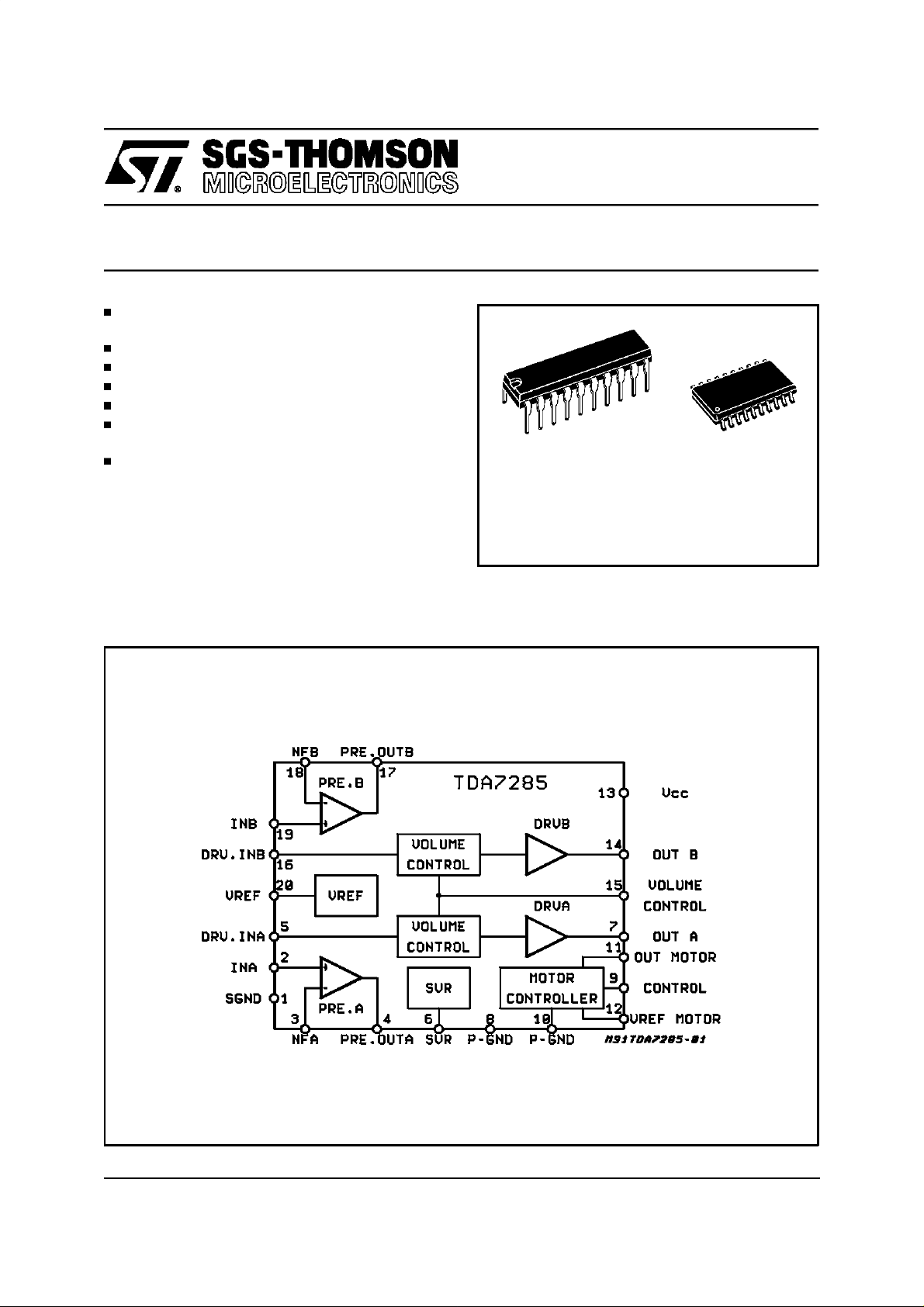
The TDA7285 is a monolithic integrated circuit
designed for the portable players market and assembled in a plastic DIP20 and SO20. The internal functions are: preamplifier, DC volume con-
BLOCK DIAGRAM
TDA7285
MOTOR SPEED CONTROLLER
DIP20 SO20
ORDERING NUMBERS:
TDA7285 TDA7285D
trol, headphone driver and motor speed controller.
May 1997
1/11
TDA7285
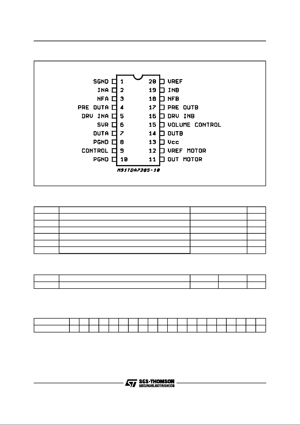
PIN CONNECTION
(Top view)
ABSOLUTE MAXIMUM RATINGS
Symbol Parameter Value Unit
Supply Voltage 8 V
S
Maximum Output Current 70 mA
Maximum Motor Current 700 mA
Total Power Dissipation T
tot
Operating Temperature -20 to +70
op
=90°C 0.9 W
amb
Storage and Junction Temperature -40 to 150 °C
C
°
I
Omax
I
m max
P
T
T
stg,Tj
V
THERMAL DATA
Symbol Description SO20 DIP20 Unit
R
th j-amb
DC CHARACTERISTICS
V
= 0; VOL. Control = V
i
Terminal No 1234567891011121314151617181920
Term. Volt.(V) 0 1.5 1.5 1.5 1.5 2.7 1.4 0 2.8 0 1.6 3 3 1.4 1.5 1.5 1.5 1.5 1.5 1.5
Thermal Resistance Junction-ambient 150 100 °C/W
=25°C; VS= 3V; RL=32Ω(Headphone)and RL= 10KΩ (Preamplifier);
(T
amb
).
ref
2/11
TDA7285
ELECTRICAL CHARACTERISTICS
= 3V; RL=32Ω, Vol. Control = 2/3 V
(V
S
ref (pin20);Tamb
=25°C;f =
1KHz; unless otherwise specified
Symbol Parameter Test Condition Min. Typ. Max. Unit
V
S
I
d
Supply Range 1.8 6 V
Total Quiescent Drain Current 15 22 mA
PLAYBACKAMPLIFIER
G
vo
G
v
V
O
THD Total Harmonic Distortion V
I
b
C
t
e
n
SVR1 Ripple Rejection R
Open Loop Gain 70 dB
Close Loop Gain 33 dB
Output Voltage THD = 1% 600 750 mV
= 330mVrms 0.05 0.25 %
O
Bias Current 3
Cross Talk RS= 2.2KΩ;VO= 330mVrms 74 dB
Total Input Noise RS= 2.2KΩ; B =22Hz to 22KHz 1.2 µV
= 2.2KΩ; Vr = 100mVrms
S
f = 100Hz; C
SVR
= 100µF
50 dB
HEADPHONEDRIVER
V
DC
P
O
P
O1
G
V
THD Total Harmonic Distortion P
C
t
SVR2 Ripple Rejection R
Output DC Voltage 1.4 V
Output Power THD = 10% 20 30 mW
Transient Output Power THD = 10% RL=16
Ω
50 mW
Close Loop Gain PO= 5mW 31 dB
Volume Control range 66 75 dB
= 5mW 0.3 1 %
O
Cross Talk PO=5mW;RS= 10K
= 600Ω; Vr = 100mV
S
f = 100Hz; C
SVR
= 100µF
Ω
50 dB
47 dB
MOTOR SPEEDCONTROL
A
µ
V
ref
Motor Reference Voltage (pin 12) 0.18 0.20 0.22 V
K Shunt Ratio I
Residual Voltage Im= 100mA 0.13 0.30 V
Line Regulation Im= 100mA;
S
Voltage Characteristics of Shunt
V
S
Ratio
Load Regulation Im= 30 to 200mA 0.015 0.08 %/mA
m
Current Characteristics of Shunt
I
m
Ratio
Temperature Characteristics of
amb
Reference Voltage
Temperature Characteristics of
T
amb
Shunt Ratio
∆ V
∆ V
∆ V
V
∆ K
V
∆ K
K
V
∆ K
K
ref
K
ref
ref
ref
V
ref
ref
⁄ ∆
sat
⁄ ∆ V
⁄ ∆
⁄ ∆I
⁄ ∆
⁄ ∆ T
= 100mA 45 50 55 -
m
0.20 0.8 %/V
V
= 1.8 to 6V
S
Im= 100mA;
V
= 1.8 to 6V
S
0.80 3 %/V
Im= 30 to 200mA 0.03 0.1 %/mA
Im= 100mA
T
= -20 to +60°C
amb
Im= 100mA
T
= -20 to +60°C
amb
0.04 %/°C
0.02 %/°C
3/11
TDA7285
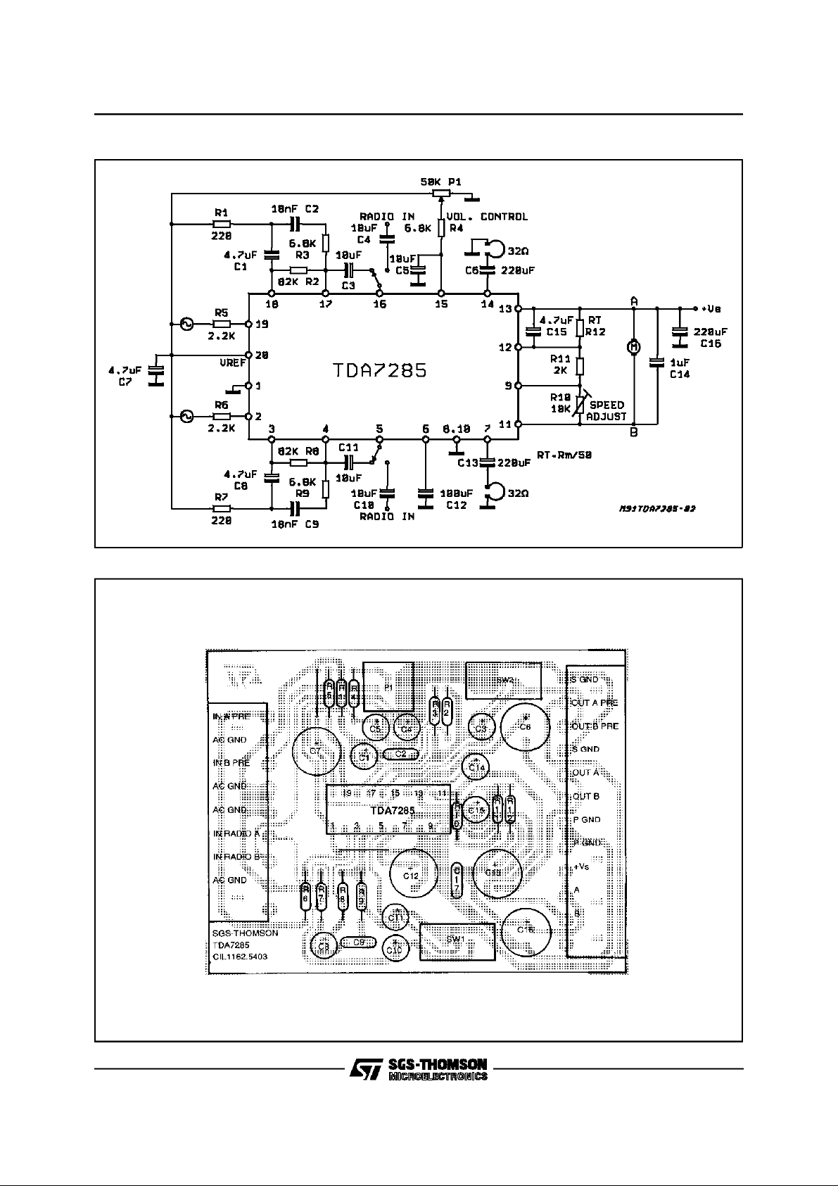
Figure 1: Test and ApplicationCircuit
Figure 2: P.C. Board and ComponentLayout of the Circuit of Figure 2 (1:1 scale)
4/11

TDA7285
Figure 3:
Figure 5:
QuiescentDrain Current vs. Supply
Voltage
ClosedLoop Gain vs. Frequency
(PREAMPLIFIER)
Figure4: ReferencevoltageV
SupplyVoltage
Figure6:
Distortionvs. Frequency
(PREAMPLIFIER)
VS=3V
= 330mVrms
V
O
R
= 10KΩ
L
/2 (pin 20) vs.
S
Figure 7: Supply Voltage Rejection vs.
Frequency(PREAMPLIFIER)
V
=3V
S
= 2.2KΩ
R
S
V
= 100mVrms
R
= 100µF
C
SVR
Figure8:
QuiescentOutput Voltage vs. Supply
Voltage(DRIVER)
5/11

TDA7285
Figure 9:
ClosedLoop Gain vs. Frequency
(DRIVER)
Figure 11: Distortionvs. Output Power (DRIVER)
Figure10: OutputPower vs. SupplyVoltage
(DRIVER)
Figure12:
Distortionvs. Frequency(DRIVER)
Figure 13: Supply VoltageRejectionvs.
Frequency(DRIVER
VS=3V
= 600Ω
R
S
V
= 100mVrms
R
= 100µF
C
SVR
6/11
Figure14:
VolumeControl (0dB = 10mW;
V
S
= 3V; R
= 50KΩ;RL=32Ω;
VOL
f = 1KHz) (DRIVER)

TDA7285
Figure 15:
Figure 17:
ReferenceVoltage (Pin 12) vs. Supply Voltage (MOTOR)
SuntRatio vs. Load Current (MOTOR)
Figure16:
Figure18:
ShuntRatio vs. Supply Voltage(MO-
TOR)
SaturationVoltage vs. Load Current
(MOTOR)
Figure 19:
SpeedVariations vs. Supply Voltage
(MOTOR)
Figure20:
SpeedVariations vs. Motor Current
(MOTOR)
7/11

TDA7285
APPLICATIONINFORMATION
Figure 21.
R
T
R
R
T
S
K
B
− R
(1+
.
M
1
K
)+V
)]
ref
Eg= RTId+ IM(
R
b
[1+
R
hasto be adjustedso that the applied voltage
S
is suitable for a given motor, the speed is then
V
M
R
+
S
linearly adjustablevaring R
The value R
R
T (max.)>K(min.)*RM (min.)
if R
T (max.)
iscalculatedso that
T
>K*RM, instabilitymay occur.
The values of C15 (4.7µF typ.) and C14 (1µF
typ.) depend on the type of motorused. C15 adjusts WOW and flutter of the system. C14 suppressesmotor spikes.
8/11

SO20 PACKAGEMECHANICAL DATA
TDA7285
DIM.
MIN. TYP. MAX. MIN. TYP. MAX.
A 2.65 0.104
a1 0.1 0.3 0.004 0.012
a2 2.45 0.096
b 0.35 0.49 0.014 0.019
b1 0.23 0.32 0.009 0.013
C 0.5 0.020
c1 45 (typ.)
D 12.6 13.0 0.496 0.512
E 10 10.65 0.394 0.419
e 1.27 0.050
e3 11.43 0.450
F 7.4 7.6 0.291 0.299
L 0.5 1.27 0.020 0.050
M 0.75 0.030
S 8 (max.)
mm inch
9/11

TDA7285
DIP20 PACKAGE MECHANICAL DATA
DIM.
MIN. TYP. MAX. MIN. TYP. MAX.
a1 0.254 0.010
B 1.39 1.65 0.055 0.065
b 0.45 0.018
b1 0.25 0.010
D 25.4 1.000
E 8.5 0.335
e 2.54 0.100
e3 22.86 0.900
F 7.1 0.280
I 3.93 0.155
L 3.3 0.130
Z 1.34 0.053
mm inch
10/11

TDA7285
Information furnished is believed to be accurate and reliable. However, SGS-THOMSON Microelectronics assumes no responsibility for the
consequences of use of such information nor for any infringement of patents or other rights of third parties which may result from its use. No
license is granted by implication or otherwise under any patent or patent rightsof SGS-THOMSON Microelectronics. Specificationmentioned
in this publication are subject to change withoutnotice. This publication supersedes and replaces all information previously supplied. SGSTHOMSON Microelectronics products are not authorized for use as critical components in life support devices or systems without express
written approval of SGS-THOMSON Microelectronics.
1997SGS-THOMSON Microelectronics – Printed in Italy– All Rights Reserved
SGS-THOMSON Microelectronics GROUPOF COMPANIES
Australia - Brazil - Canada - China - France - Germany - HongKong - Italy - Japan - Korea - Malaysia - Malta - Morocco - The Netherlands-
Singapore - Spain - Sweden - Switzerland- Taiwan - Thailand - UnitedKingdom - U.S.A.
11/11
 Loading...