

RECORD/PLAYBACK CIRCUIT WITH ALC
WIDE OPERATING SUPPLY VOLTAGE (3V
to 12V)
VERYLOW INPUT NOISE (V
INTERNAL COMPENSATION FOR HIGH
GAIN APPLICATION (DOUBLE SPEED RECORDING)
BUILT-INALC CIRCUITRY
GOODSVR
DC CONTROLLED SWITCHES FOR MUTE
OR EQUALIZATION SWITCHING FUNCTIONS
DESCRIPTION
The TDA7284 is a monolithic integrated circuit in
a DIP/SO-14designed for 6V, 9V and 12VAC/DC
portable cassetteequipmentapplication.
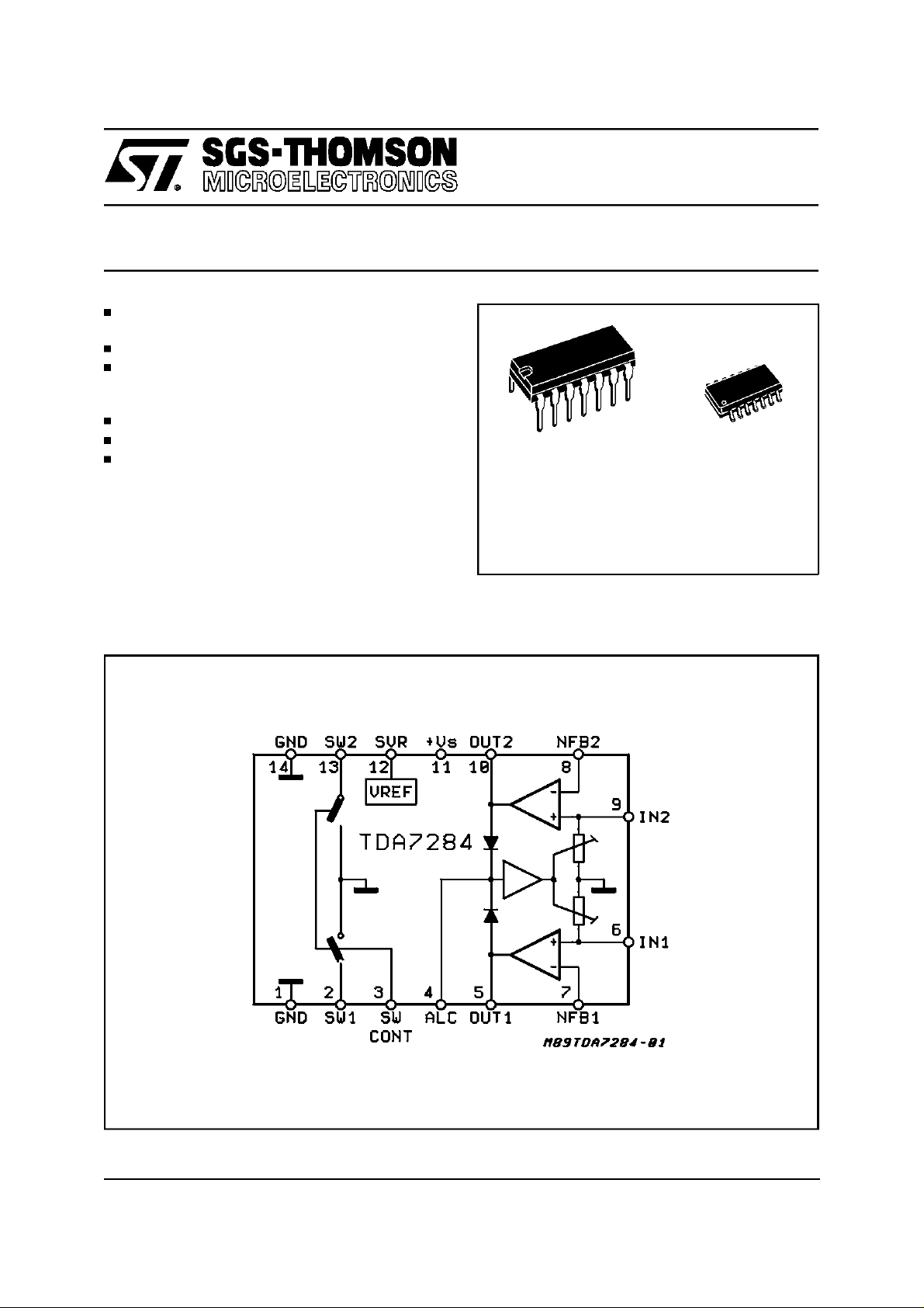
BLOCK DIAGRAM
= 1.2µV)
I
TDA7284
DIP14 SO14
ORDERING NUMBER:
TDA7284 TDA7284D
May 1997
1/14

TDA7284
PIN CONNECTION (Topview)
ABSOLUTE MAXIMUM RATINGS
Symbol Parameter Value Unit
V
T
T
stg,Tj
S
OP
Supply Voltage 14 V
Operating Temperature Range -20 to 70
°
Storage and Junction Temperature Range -40 to 150 °C
C
THERMAL DATA
Symbol Description S014 DIP14 Unit
R
th j-amb
DC CHARACTERISTICS (T
Thermal Resistance Junction-ambient Max 200 120
=25°;VS= 6V;Vi= 0V;Ri= 10KΩ; ALC= OFF)
amb
Terminal No. 1 2 3 4567891011121314
Terminal Voltage(V) 0 0 0 0 2.6 0 1.3 1.3 0 2.6 6 4.6 0 0
C/W
°
2/14
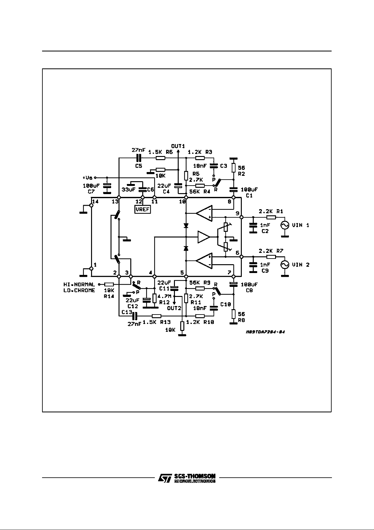
Figure 1: Test and ApplicationCircuit
TDA7284
3/14
TDA7284
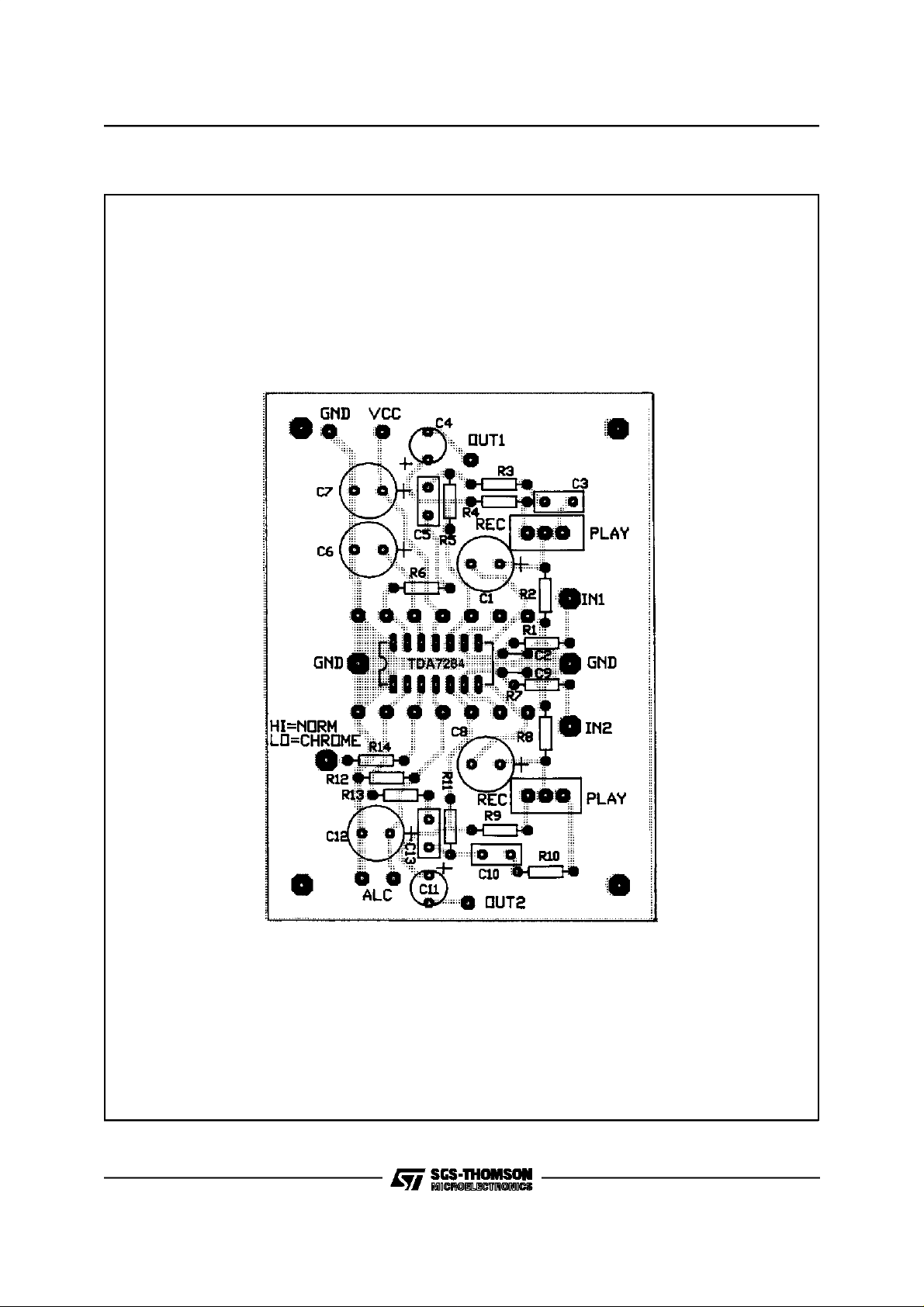
Figure 2: P.C.Board and ComponentLayout of the Circuit of Fig. 1 (1:1 scale).
4/14
TDA7284
ELECTRICAL CHARACTERISTICS (VS= 6V, T
=25°C unless otherwise specified refer to test cir-
amb
cuit)
Symbol Parameter Test Condition Min. Typ. Max. Unit
V
S
I
d
E
n
R
I
G
O
V
O
THD Total Harmonic Distortion VO=1V
CB Channel Balance ALC ON 0 2 dB
SVR Supply Voltage Rejection f = 120Hz, C
CS Cross-talk ALC OFF 70 dB
Pin 3 Turn Off Threshold I
Pin 3 Turn On Threshold 1.7 2.25 V
Pin 3 Turn On Saturation R
Supply Voltage 3 12 V
Quiescent Current 4.5 8 mA
Input Noise Rg= 2.2KΩ
1.2 µV
BW = 22Hz to 22kHz
Input Resistance 30 50 70 KΩ
Open Loop Gain 65 78 dB
Output Voltage THD < 1% ALC OFF
ALC ON
ALC = ON VI= 100mV
rms
ALC Range
= 3dB 47 dB
V
∆
O
=33µF
V
= 100mV, Rg= 10K
R
SVR
Ω
1.2
0.7
1.8
0.9 1.1
0.1
0.3
0.5
1
50 dB
ALC = Off
=<1µA 0.8 1.3 V
O
= 10KΩ 0.1 0.2 V
L
V
rms
V
rms
%
%
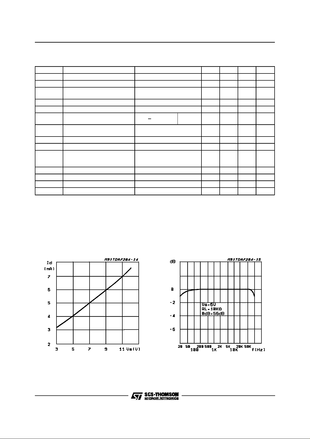
Figure 3: DrainCurrent vs. Supply Voltage Figure 4: RecordingClosed Loop Gain vs.
Frequency
5/14

TDA7284
Figure 5: PlaybackClosed Loop Gain vs
Frequency
Figure6: NormalizedOutput Voltagevs. Supply
Voltage
Figure 7: OutputVoltagevs. Input Voltage Figure8: OutputVoltagevs. Input Voltage
Figure 9: OutputVoltagevs. Input Voltage
6/14
Figure10: Distortion vs. Input Voltage

TDA7284
Figure 11: Distortion vs. Input Voltage
Figure12: SVR vs.Frequency (ALC = Off)
Figure13: Crosstalkvs. Frequency(ALC = Off) Figure 14: Crosstalkvs. Frequency (ALC= Off)
7/14
TDA7284
CIRCUIT DESCRIPTION
OPERATIONALAMPLIFIER
The operational amplifier consists essentially of a
very low noise input stage decoupled from the
Figure 15
single-endedoutput stage by means of an emitter
follower (fig. 15 ).
The compensations provided in order to have
high gain bandwith product allowing the use for
doublespeed recordingapplication.
AUTOMATICLEVEL CONTROL SYSTEM(ALC)
This system maintainsthe level of the signal to be
recorded at a value which prevents saturation of
the tape and which optimizes the signal to noise
ratio even there are notable variations in the input
signal.
Before presentingthe ALC circuit of TDA7284 it is
worth describing the operation of the automatic
level control as a system.A diagram showing the
basis of operationis givenin fig.16.
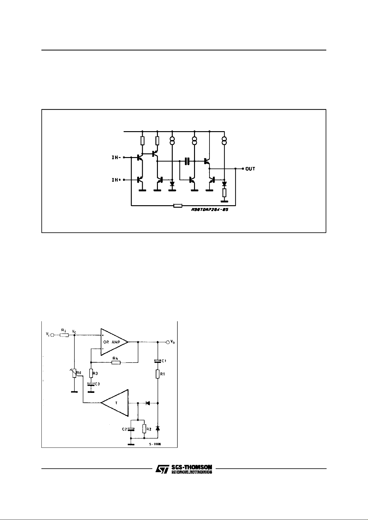
Figure 16: BasicDiagram of the ALC stage
This consists of an amplifier(op-amp) havingconstant gain (G
= 1+R4/R3),which in feedback
V
transformsoutput signal level information (usually
by means of a peak-to-peak detector) into a continuous voltage which drives the networks indicatedby T and Rd.
The element T transforms the continuous voltage
level into a signal capable of modifying the circuit
conditionssymbolizedby variableresistor Rd.
The value assumed by the resistor Rd is a function of the output signal level Vo and is such that
the voltage Vc at the input of the op-amp is constant,even variations of Vi are present.Obviously
if Vo is less than a certain value the system is not
controlled.
In thiscase :
V
I=VC=VO/GV
(GVisthe gain of the op-amp)
For the TDA7284 the value of V
belowwhich the
o
systemis not controlledis around 1 Vrms.
Let us now consider the speed of response of the
system (when controlled) to positiveand negative
changes of the input signal i.e. the limiting
time,the time for return to nominal level (1 Vrms)
and the recoverytime.
8/14
Limiting time, and time for return to nominal
level.
Let us supposethat at certain moment T
, the in-
o
put signalincreases by+∆Vi as shownin fig. 17.

Figure 17: Limitingand LevelSetting Time
Usually such an increase drives the op-amp into
saturationand the time for whichit remains in this
conditionis calledthe limiting time(T1).
T1 depends on the relationship between the external capacitances,the time constantT=R1•C1,
the supply voltage and the signal variation.
The criteria for choosing the length of T1 are the
result of several compromises. In particular if T1
is too long, there will be audible distortion during
playback (during T1 the output is a square
wave),and if it is too short, the sensation of increased level will be lost while dynamic compression phenomenaand instabilitymay occur.
The time for return to nominal level is defined as
the total time between the instant To and the instant in which the output reassumes the nominal
value. Thistime (Ts) is roughlyequal to5 • T1.
On the basisof tests carried out it has been found
that a musical signal with high dynamic range
TDA7284
=+40 dB) is to be recorded, the bestvalue of
(∆V
I
Ts is between200 and300ms.
Recoverytime.
let us nowsuppose that at the instantTo the input
signal decreasesof ∆Vi (fig. 18).
Figure18: Recovery Time
The recovery time (Trec) is defined as the time
between the instant To and the instant in which
the outputsignal returnsto the nominallevel.
This time depends essentially on the discharge
time constant of R2 •C2 ( see fig. 16) and on the
size of the step -∆Vi. In this case too, if this time
is too long the signal to noise ratio on the tapedeteriorates.
If it is too short the sensation of the low signal
levelis lostduring playback.
The ALC system of the TDA7284
Fig. 16 becomesthe following(fig. 19) where the
Figure 19
9/14
TDA7284
peak-to-peak detector of fig. 16 is now inside the
Figure20
broken line 1 while the system which allows a dinamic resistance varying with the DC voltage
level (i.e. inversely proportional to the op-amp
output signal),isinsidethe broken line2.
It should be noted that the generator resistance
Ri has no influence on the controlled voltage
value Vc, although its value should be between 1
and 47 Kohm.
The lower limit is determined by the minimum dynamic resistance of 10 ohm and therefore to
have a controlrange of 40 dB for the input signal,
Ri must be greather than 1.5 Kohm.
The upper limit results from the necessity to limit
the attenuation of the signal by the input impedance of theop-amp.
to the IC, while the tape selector switch can be at
a remote location, hence reduce the chances of
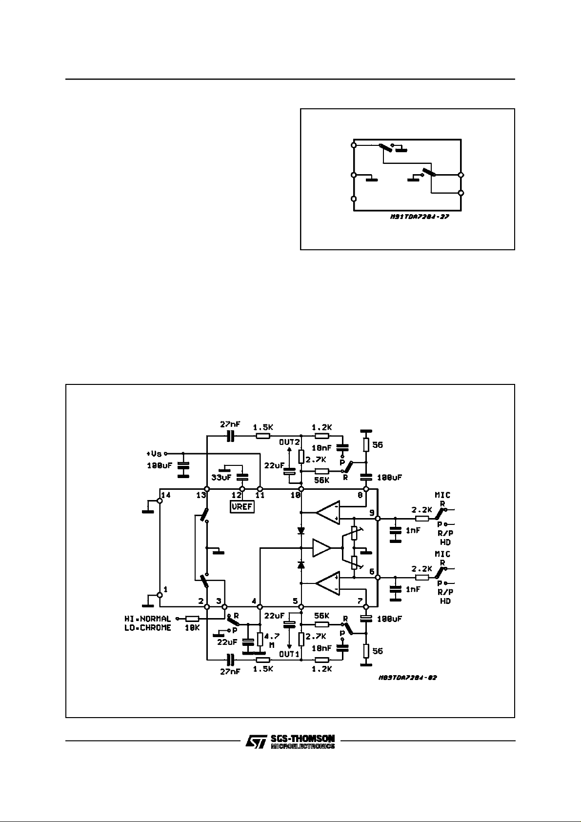
Switches
Two DC-controlled switches are also included in
the chip (fig.20 )
Fig. 19 shows the typical application circuit of the
TDA7284 utilizing the equalization switch for normal or chrome tape playback equalization.The
advantage is the components can be placed near
noise and oscillation due to components layout.
Another advantage is that only one pole is
needed for the tape selector switch as compared
to the two poles needed by conventional circuits
(one separatepole for each channel).
Fig. 22 shows the use of the switches to obtain
the mute function.
Figure 21: ApplicationCircuitwith DC Switchingof Normal/ChromeTapeEqualization
10/14

Figure 22: ApplicationCircuit with OutputMuting
TDA7284
SVR
A refernce circuit is enclosed to provide a stable
voltage and to supply a stable current to all cur-
rent mirrors.
SVR capacitor is also connected to this block for
good ripplerejection.
11/14

TDA7284
DIP14 PACKAGE MECHANICAL DATA
DIM.
MIN. TYP. MAX. MIN. TYP. MAX.
a1 0.51 0.020
B 1.39 1.65 0.055 0.065
b 0.5 0.020
b1 0.25 0.010
D 20 0.787
E 8.5 0.335
e 2.54 0.100
e3 15.24 0.600
F 7.1 0.280
I 5.1 0.201
L 3.3 0.130
Z 1.27 2.54 0.050 0.100
mm inch
12/14

SO14 PACKAGEMECHANICAL DATA
TDA7284
DIM.
MIN. TYP. MAX. MIN. TYP. MAX.
A 1.75 0.069
a1 0.1 0.2 0.004 0.008
a2 1.6 0.063
b 0.35 0.46 0.014 0.018
b1 0.19 0.25 0.007 0.010
C 0.5 0.020
c1 45° (typ.)
D 8.55 8.75 0.336 0.344
E 5.8 6.2 0.228 0.244
e 1.27 0.050
e3 7.62 0.300
F 3.8 4.0 0.15 0.157
L 0.5 1.27 0.020 0.050
M 0.68 0.027
mm inch
S8°(max.)
13/14

TDA7284
Information furnished is believed to be accurate and reliable. However, SGS-THOMSON Microelectronics assumes no responsibility for the
consequences of useof such information nor for any infringement of patents or other rights of third partieswhich may result from its use. No
license is granted by implicationor otherwise under any patentor patent rights of SGS-THOMSON Microelectronics. Specification mentioned
in this publication are subject to change without notice. This publication supersedes and replaces all information previously supplied. SGSTHOMSON Microelectronics products are not authorized for use as critical components in life support devices or systems without express
written approval ofSGS-THOMSON Microelectronics.
Australia - Brazil - Canada - China - France -Germany - HongKong - Italy - Japan - Korea - Malaysia- Malta- Morocco - The Netherlands -
1997 SGS-THOMSON Microelectronics– Printed in Italy– All Rights Reserved
Singapore - Spain - Sweden - Switzerland- Taiwan- Thailand - United Kingdom - U.S.A.
SGS-THOMSON Microelectronics GROUP OF COMPANIES
14/14
 Loading...