

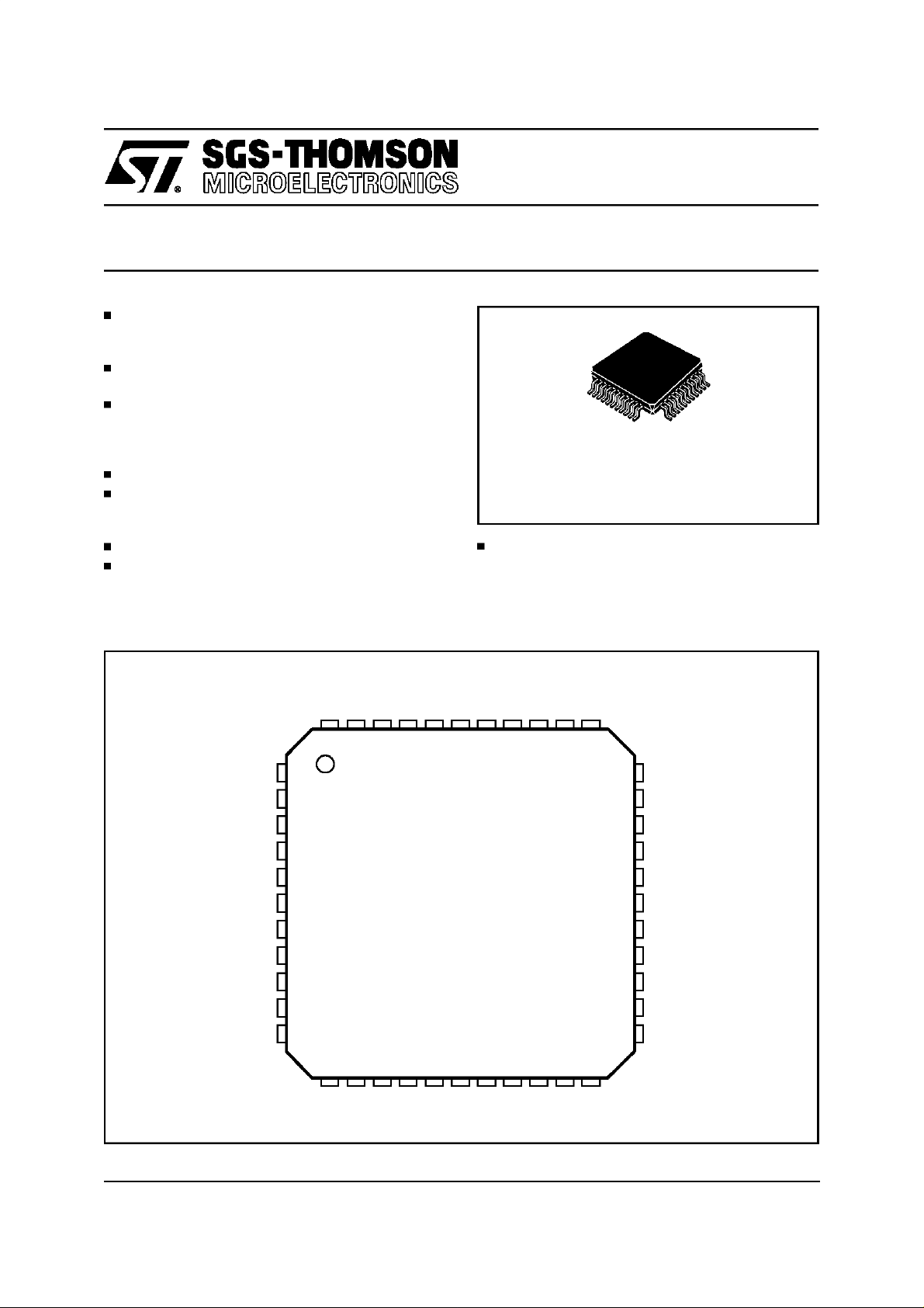
HIGH-EFFICIENCYCD ACTUATOR DRIVER
WIDE OPERATIVE SUPPLY RANGE (1.6 to
5V) LOW VOLTAGE OPERATION CAPABILITY
4 LOAD DRIVING VOLTAGES PWM REGULATED (STEPDOWNFROM BATTERY)
LOW ON RESISTANCE H BRIDGES
(2 x 1.6Ω MAX + 2 x2.5Ω MAX) FOR:
– FOCUSAND TRACKING ACTUATORS
– SLEDGEAND SPINDLEMOTORS
SYNCHRONIZABLESAWTOOTHOSCILLATOR
CONFIGURABLE DC/DC CONVERTER FOR
ADJUSTABLE MAIN POWER SUPPLY, WITH
LOW ON RESISTANCE(0.4Ω MAX)SWITCH
GENERALENABLEINPUT
ADJUSTABLE WATCH DOG AND DELAYED
POWERON RESET FUNCTIONS
PIN CONNECTION
TDA7278
PQFP44
ADJUSTABLE COMPARATORS FOR BATTERY LOW AND BATTERY EMPTY DETECTION
HIN2
H OUT 2A
FLIN 2
VBAT
FLIN 1
GND
H OUT 1A
HIN1
H OUT 1B
OUT
VHIGH
H OUT 2B
ERROR 1
ERROR 2
BEMP
44 43 42 41 3940 38 37 36 35 34
1
2
3
4
5
6
7
8
9
10
12 13 14 15 16
INP
IRC
SSCAP
VCPU
VCON
BLOW
OUT1
VREF(2)
VREF(1)
171118 19 20 21 22
VBG
OUT2
RESET
ERROR 4
CRES
ERROR 3
WDINP
H OUT 4B
STCAP
33
32
31
30
29
28
27
26
25
24
23
D94AU112A
HIN4
H OUT 4A
FLIN 4
VBAT
FLIN 3
GND
H OUT 3A
HIN3
H OUT 3B
ENABLE
SYNC
March 1997
1/15
TDA7278
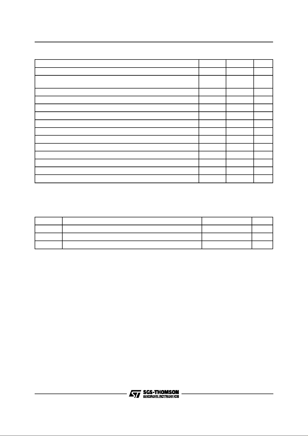
ABSOLUTE MAXIMUM RATINGS (25°C)
Pin Name Min Max Unit
HIN 1, HIN 2, HIN 3, HIN 4 -0.4 8 V
HOUT 1A, HOUT 2A, HOUT 3A, HOUT 4A, HOUT 1B, HOUT 2B, HOUT 3B,
HOUT 4B
FLIN 1, FLIN 2,FLIN 3, FLIN 4 -0.4 10 V
ERROR 1, ERROR 2, ERROR 3, ERROR 4, -0.4
V
BAT
V
REF 1,VREF 2
BLOW, BEMP, V
CON
OUT, VHIGH -0.4 16 V
OUT 2 -0.4 8 V
OUT 1 -0.4 16 V
SSCAP, IRC, INP -0.4 7 V
VCPU -0.4 7 V
VBG, RESET, CRES, WDINP, STCAP, SYNC -0.4 7 V
EN -0.4 8 V
-0.4 8 V
7
-0.4 8 V
-0.4 7 V
-0.4 7 V
V
* Pin1, 8, 12, 14, 20, 26 and 33 are ESD sensitive (max. voltage ±1KV)
THERMAL DATA
Symbol Parameter Value Unit
T
T
op
T
j-amb
j
Operating Temperature range –25 to 70 °C
Max. Junction Temperature 100 °C
Thermal Resistance Junction to Ambient 70 °C/W
2/15

PIN FUNCTIONS
o
N
21 WDINP
20 CRES Start up reset control for µC & watch dog time constant
19 RESET Reset output command to µC (open collector)
41 BEMP Battery empty comparator input
40 BLOW Battery low comparator input
39 VCON
24 ENABLE General Enable Input (active Low)
18 VBG Reference voltage capacitor
12 SSCAP Soft start capacitor
16 OUT 1 Switching transistor terminal high
17 OUT 2 Switching transistor terminal low
15 VCPU Regulated voltage
14 IRC Error amplifier output
13 INP Error amplifier inverting input
11 VHIGH Regulated Voltage
10 OUT Switching transistor output
22 STCAP Sawtooth toth
23 SYNC Oscillator synchronizing input
4, 30 V
6, 28 GND Power ground
38 VREF 2 Buffered reference output voltage
37 VREF 1 Reference input voltage
5 FLIN 1 Switching Output
7 HOUT 1A H bridge positive output
8 HIN 1 Regulated voltage H bridge supply
9 HOUT 1B H bridge negative output
43 ERROR 1 Error input
29 FLIN 3 Switching Output
27 HOUT 3A H bridge positive output
26 HIN 3 Regulated voltage H bridge supply
25 HOUT 3B H bridge negative output
35 ERROR 3 Error input
3 FLIN 2 Switching output
2 HOUT2A H bridge positive output
1 HIN 2 Regulated voltage H bridge supply
44 HOUT 2B H bridge negative output
42 ERROR 2 Error input
Name Function
Watch dog input - AC coupled to WDµcontroller output
(Disabled when connected to GND)
Battery level control output
VCON = Z VBEMP > VBCON > VBG
VCON = 1 VBEMP > VBG > VBLOW
VCON = 0 VBG > VBEMP > VBLOW
BAT
Power supply voltage
TDA7278
Watch dog & reset
circuit
Battery control circuit
Band Gap Reference
VCPU DC-DC
converter
Vhigh Boost DC-DC
Converter
Oscillator
Focus actuator step
down converter
& H bridge
Tracking actuator
step down converter
& H bridge
Spindle motor step
down converter
& H bridge
3/15
TDA7278
ELECTRICALCHARACTERISTICS (T
amb
=25°C, V
= 1.6Vunless otherwisespecified)
BAT
Symbol Parameter Test Condition Min. Typ. Max. Unit
V
BAT
Power Supply
(T
amb
=25to70°C)
Config. in fig. 3a: V
Config. in fig. 3a: V
CPU
CPU
<4V
>4V
Config. in fig. 3b
Config. in fig. 3c
1.6
1.6
V
+0.3
CPU
1.6
V
CPU
4
4
4
Stand-by condition
Power Supply
(T
amb
=25to60°C)
Config. in fig 3a
Config. in fig. 3a
Config. in fig. 3b
Config. in fig. 3c
1.6
V
+0.3
CPU
1.6
4
V
CPU
5
5
Stand-by condition
Current Consumption from
V
(1)
CPU
Current Consumption from
(3)
V
BAT
Leakage Current in stand-
Config. in fig 3a
CPU =5V 5 mA
V
1.5 mA
V
=5V 20 µA
BAT
5.5
by condition
V
HIGH
V
CPU
Output Voltages V
(adj)
R
ofDC/DCConverterSwitch I = 1A 0.25 0.4 Ω
ON
Max Output Current from
V
CPU
Voltage Ripple on V
CPU
Oscillator - freefreq.
- sync. freq
- ∆ free freq.
H_bridge
VCPU < 4.5V Config. fig 3a 150 mA
STCAP = 470pF
.
V
= 1.6 to 5V
BAT
I = 100mA
- Ron, actuators (CH 1,3)
- Ron, motors (CH 2,4)
PWM Circuit
I = 100mA
- Ron, actuators
- Ron, motors
V
Reference Voltage 1.22 1.28 1.34 V
BG
Load Regulation I
Line Regulation V
=-10to+10µA; -30 30 mV
LOAD
=1.6to5V 30 mV
BAT
AV Bridge gain From Error to H
IN
+4
V
BAT
BAT
+7 V
BAT
2.4
200
80
1.0
1.6
0.5
0.8
2.8 3.6 4.5
+12
5
180
20
1.6
2.5
0.8
1.25
K Reset Time Coefficient note 2 7.4 11 17.2 msec/µF
Z
Error Impedance Inputs 26 40 kΩ
IN
V
Load Regulation I
REF2
V
Impedance 750 k
REF1
=-1to+1mA –30 30 mV
LOAD
WINDIP Impedance 30 k
BEMP & BLOW
0.55 0.65 0.75 V
intervention threshold
RESET Voltage Saturation I
VCON Voltage Saturation I
(1): all the 4 PWM outputs switched off.
=-100µA 200 mV
LOAD
=-100µA
LOAD
I
=100µAV
LOAD
CPU
-200
200 mV
V
V
V
V
V
V
V
V
V
V
V
KHz
KHz
KHz
Ω
Ω
Ω
Ω
Ω
Ω
mV
(2) T
(3) Allthe 4 PWM outputswitched OFF, auxiliary and main DC/DC converters polarized but not switching
= width of the Reset pulse on pin 19 = K ⋅ C,where C is the capacitance on pin 20 (C
RESET
To avoid reset, the frequency of watch dog pulses must be greater than (3 ⋅ T
RESET
).
RES
-1
)
4/15

Figure 1: Block Diagram.
22
ST CAP
38
VREF (2)
11
VHIGH
10
OUT
SYNC
23 4 30 37 4335
OSCILL
VBAT
VBAT
Vbg
TDA7278
VREF (1)
ERROR 3
ERROR 1
VHIGH
DRIV
ER
VHIGH
+
-
S
+
DRIV
Q
R
VHIGH
DRIV
VBAT
5
8
7
9
FL IN 1
HIN1
H OUT 1A
H OUT 1B
INP
IRC
VCPU
OUT1
OUT2
SSCAP
VBG
ENABLE
CRES
RESET
WD INP
BEMP
BLOW
VCON
VHIGH
DRIV
VHIGH
DRIV
VHIGH
DRIV
VBAT
VBAT
VBAT
29
26
27
25
44
31
33
32
34
3
1
2
FL IN 3
HIN3
H OUT 3A
H OUT 3B
FL IN 2
HIN2
H OUT 2A
H OUT 2B
FL IN 4
HIN4
H OUT 4A
H OUT 4B
13
14
ER
-
15
VCPU
VHIGH
DRIV
REFERENCE
and
THERMAL
Vbg
+
VBAT
Vbg
Vbg/2
VbgCONTROL
Vbg/2
+
-
Vbg/2
+
-
+
+
+
16
17
12
18
24
20
19
21
41
40
39
+
VHIGH
-
ER
-
ER
-
DRIV
+
VHIGH
DRIV
+
VHIGH
DRIV
VHIGH
DRIV
S
Q
R
VHIGH
DRIV
S
Q
R
VHIGH
DRIV
S
Q
R
62842 36
GND
GND
ERROR 2
ERROR 4
D94AU078B
5/15

TDA7278
Figure 2: Test Circuit
ST CAP
470pF
10µF
10µF
VREF (2)
VHIGH
VBAT
47µH
AUXIL.
STEP UP
OUT
VBAT
VREF (1)
ERROR 3
SYNC
23
22
OSCILL
38
11
10
430
37 4335
Vbg
ERROR 1
VHIGH
DRIV
ER
VHIGH
+
-
S
-
+
DRIV
Q
R
VHIGH
DRIV
VBAT
5
8
7
9
FL IN 1
HIN1
H OUT 1A
H OUT 1B
100µH
10µF
FOCUS
ACTUATOR
FEEDBAKC
&
COMPENSATION
NETWORK
(see fig.4)
STEP
LP
or
STEP DOWN
STRUCTURE
(see fig.3)
2µF
100nF
1µF
VBAT BEMP
INP
IRC
VCPU
OUT1
OUT2
SSCAP
VBG
ENABLE
CRES
RESET
WD INP
BLOW
VCON
VHIGH
DRIV
VHIGH
DRIV
VHIGH
DRIV
VBAT
VBAT
VBAT
29
26
27
25
44
31
33
32
34
3
1
2
FL IN 3
HIN3
H OUT 3A
H OUT 3B
FL IN 2
HIN2
H OUT 2A
H OUT 2B
FL IN 4
HIN4
H OUT 4A
H OUT 4B
100µH
10µF
TRACKING
ACTUATOR
100µH
10µF
SPINDLE
M
MOTOR
100µH
10µF
SLEDGE
M
MOTOR
13
14
ER
-
+
15
VCPU
VHIGH
DRIV
REFERENCE
and
THERMAL
CONTROL
Vbg
+
VBAT
Vbg
Vbg
Vbg/2
+
-
Vbg/2
+
-
16
17
12
18
24
20
19
21
41
40
39
VHIGH
+
-
ER
+
-
ER
+
-
DRIV
-
+
VHIGH
DRIV
-
+
VHIGH
DRIV
VHIGH
DRIV
S
Q
R
VHIGH
DRIV
S
Q
R
VHIGH
DRIV
S
Q
R
6/15
62842 36
GND
ERROR 2
ERROR 4
D94AU111A

Figure 3: DC – DC ConverterConfiguration.
VCPU
VBAT
TDA7278
15
L
C
16
OUT 1
OUT 2
17
VHIGH
DRIV
D94AU081B
a) step-up
VCPU
15
VBAT
16
OUT 1
L
OUT 2
C
17
VHIGH
DRIV
D94AU082B
b) step-down
VCPU
15
VBAT
VHIGH
C
16
OUT 1
DRIV
OUT 2
17
D94AU083B
c) withtransformer
7/15
TDA7278
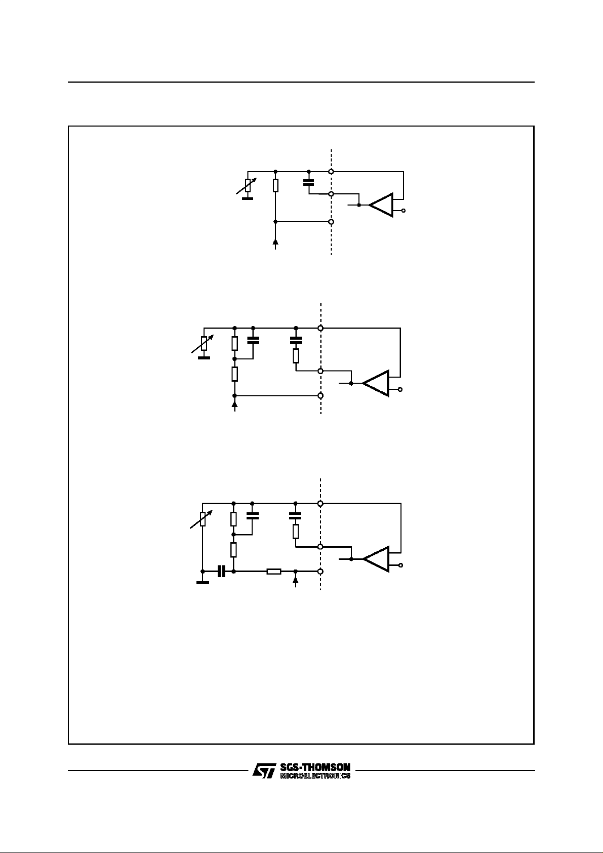
Figure 4: DC – DC Converter:Feedback andCompensationNetworks.
INP
IRC
VCPU
13
14
15
13
VCPU
RESISTOR
SETTING
R
4
C
R
f
a) Dominant Pole Compensation
INP
Vbg
D94AU113A
R
4
R
3
R
2
C
C
f
2
R
f
VCPU
IRC
14
-
15
+
D94AU114A
b) Extended Bandwidth 2 zero, 2 pole compensation
INP
13
R
4
R
3
R
2
C
1
C
C
f
2
R
f
VCPU
R
1
IRC
14
-
15
+
D94AU115A
c) Extended Bandwidth 2 zero, 3 pole compensation
Vbg
Vbg
8/15

SUGGESTEDVALUES FOR OUTPUT FILTER AND COMPENSATION NETWORK
TDA7278
DC- DC COVERTER
CONFIGURATIONS
STEP-DOWN
STEP-UP
AND
TRANSFORMER
OUTPUT FILTER (see fig. 3) COMPENSATION (see fig. 4)
a) DOMINANT POLE
R = 50KΩ
Cf = 47nF
L=47µH
C=47µF
R4 = 35K
b) 2 ZERO, 2 POLE
R2 = 11.18K
Ω
Ω
R3 = 100 KΩ
C2 = 936pF
Rf = 16.65KΩ
Cf = 5.6nF
R4 = 70KΩ
a) DOMINANT POLE
R = 100KΩ
Cf = 220nF
R4 = 70K
Ω
c) 2 ZERO, 3 POLE
L=47µH
C=47µF
R1 = 500Ω
C1 = 18nF
R2 = 20.8KΩ
R3 = 250KΩ
C2 = 636pF
Rf = 21.4K
Ω
Cf = 7.44nF
R4 = 200KΩ
c) 2 ZERO, 3 POLE
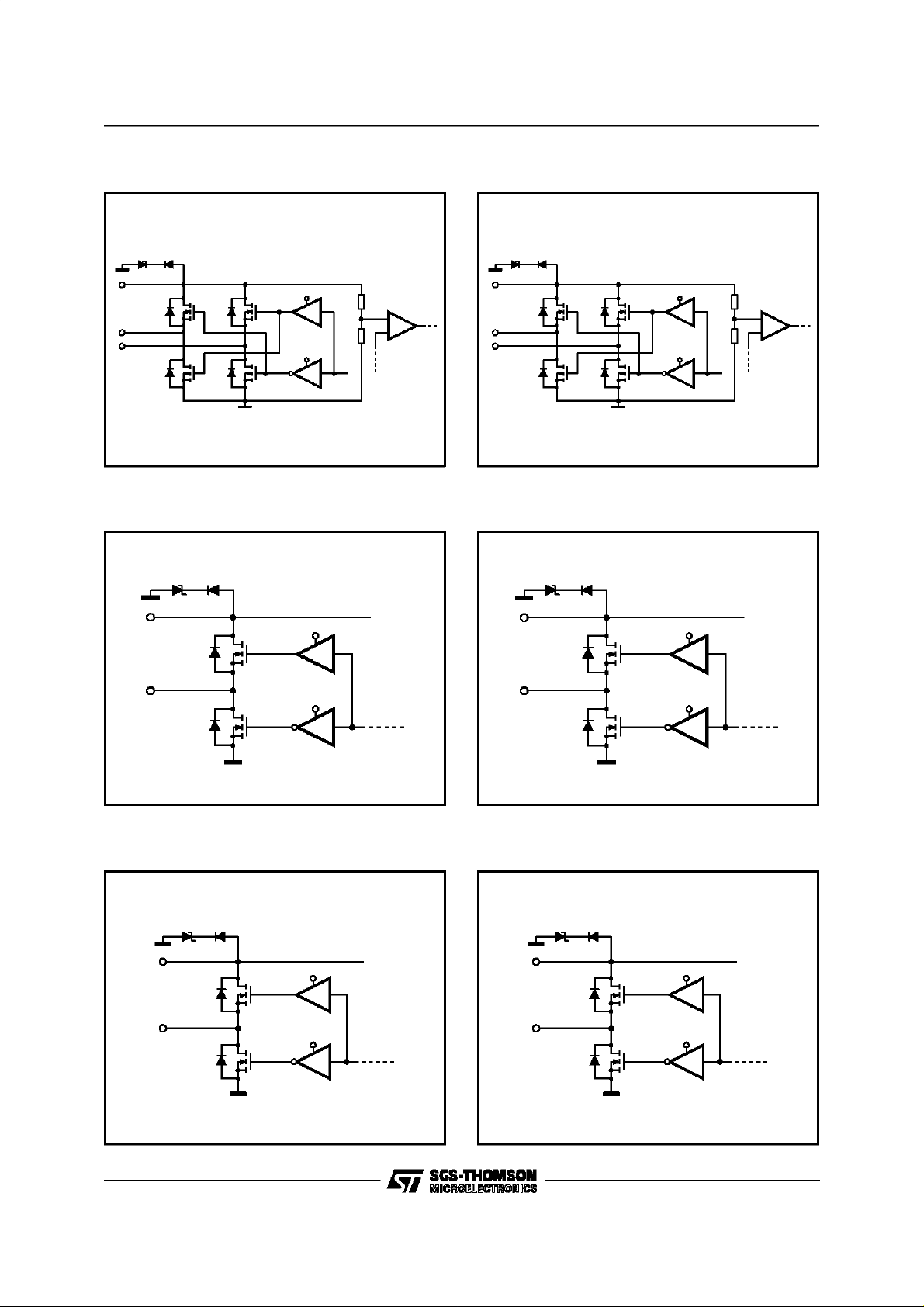
PINS: 1, 2, 44
12V
1
2
44
VHIGH
VHIGH
D96AU447A
+
-
L=11µH
C=47µF
PINS: 8,7,9
12V
8
7
9
R1 = 500Ω
C1 = 18nF
R2 = 10.4K
R3 = 250KΩ
C2 = 318pF
Rf = 21.4K
Cf = 3.7nF
R4 = 200KΩ
Ω
Ω
VHIGH
+
-
VHIGH
D96AU448A
9/15
TDA7278
PINS: 25, 26, 27
12V
26
27
25
PIN: 3
12V
4
VBAT
VHIGH
VHIGH
VHIGH
D96AU449A
PINS: 32, 33, 34
12V
33
+
-
32
34
VHIGH
+
-
VHIGH
D96AU450A
PINS: 5
12V
VBAT
4
VHIGH
PIN: 29
3
VHIGH
D96AU451
5
VHIGH
D96AU452
PINS: 31
12V
VBAT
30
29
VHIGH
VHIGH
D96AU453
12V
VBAT
30
31
VHIGH
VHIGH
D96AU454
10/15

TDA7278
PINS: 35
PIN: 42
7V
35
38
VCPU
-
+
D96AU465
PIN: 36
PIN: 43
7V
36
38
VCPU
-
+
D96AU466
PIN: 18
7V
7V
18 +
D96AU458
42
38
VBAT
-
VCPU
-
+
D96AU467
VBAT
REFERENCE
7V
PINS: 19
7V
43
38
VCPU
-
+
D96AU468
19
D96AU459
11/15

TDA7278
PINS: 20
7V
PIN: 22
7V
22
20
VCPU
VBAT
D96AU460A
D96AU462
1.8
0.7
0.6
1.3
0.6
0.2
VCPU
+
VCPU
+
VCPU
+
-
VBAT
+
VBAT
+
VBAT
+
-
PINS: 21
PIN: 23
7V
D96AU461A
7V
VCPU
VCPU
VCPU
+
-
21
23
VCPU
-
+
VCPU
D96AU463
PIN: 24
12V
12/15
24
D96AU464A
PINS: 10, 11
17V
VBATVBAT
VBAT
11
+
-
10
D96AU474

TDA7278
PINS: 12, 13, 14
13
12
14
7V
PINS: 37, 38
VBAT
VBAT
+
VBG
D96AU475
VCPU VCPU
PINS: 16, 17
VBAT
16
17
17V
D96AU476
PIN: 39
VCPU
7V
PINS: 40, 41
7V
37
+-
38
VBG
40
41
D96AU469
5V
5V
39
7V
D96AU470A
VCPU
-
+
VCPU
-
+
D96AU471
13/15
TDA7278
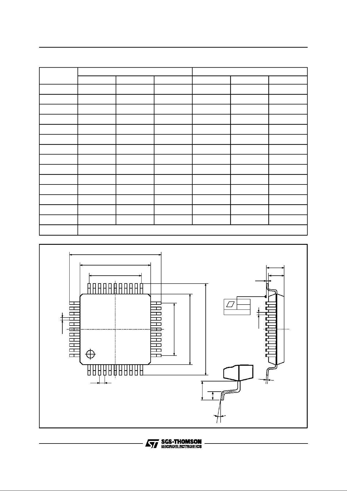
PQFP44 (10x10)PACKAGEMECHANICAL DATA
DIM.
mm inch
MIN. TYP. MAX. MIN. TYP. MAX.
A 2.45 0.096
A1 0.25 0.010
A2 1.95 2.00 2.10 0.077 0.079 0.083
B 0.30 0.45 0.012 0.018
c 0.13 0.23 0.005 0.009
D 12.95 13.20 13.45 0.51 0.52 0.53
D1 9.90 10.00 10.10 0.390 0.394 0.398
D3 8.00 0.315
e 0.80 0.031
E 12.95 13.20 13.45 0.510 0.520 0.530
E1 9.90 10.00 10.10 0.390 0.394 0.398
E3 8.00 0.315
L 0.65 0.80 0.95 0.026 0.031 0.037
L1 1.60 0.063
K0°(min.), 7°(max.)
D
D1
A1
33
34
B
44
1
e
23
11
PQFP44
22
L1
E
L
E3D3E1
12
0.10mm
.004
Seating Plane
B
K
A
A2
C
14/15

TDA7278
Information furnished is believed to be accurate and reliable. However, SGS-THOMSON Microelectronics assumes no responsibility for the
consequences of use of such information nor for any infringement of patents or other rights of third parties which may result from its use. No
license is granted by implicationor otherwise under any patentor patentrights ofSGS-THOMSON Microelectronics. Specifications mentioned
in this publication are subject to change without notice. This publication supersedes and replaces all information previously supplied.
SGS-THOMSON Microelectronics products arenotauthorized foruseas criticalcomponents in lifesupport devices or systemswithout express
written approval of SGS-THOMSON Microelectronics.
1997 SGS-THOMSON Microelectronics AllRights Reserved
Australia - Brazil - France - Germany - Hong Kong - Italy - Japan - Korea- Malaysia - Malta - Morocco - The Netherlands - Singapore -
SGS-THOMSON Microelectronics GROUP OF COMPANIES
Spain - Sweden - Switzerland - Taiwan - Thaliand - UnitedKingdom - U.S.A.
15/15
 Loading...