

HIGH PERFORMANCE MOTOR SPEED REGULATOR
TACHIMETRIC SPEED REGULATION WITH
NO NEED FOR AN EXTERNAL SPEED PICKUP
V/I SUPPLEMENTARYPREREGULATION
DIGITAL CONTROL OF DIRECTION AND
MOTORSTOP
SEPARATESPEEDADJUSTMENT
5.5V TO 18V OPERATING SUPPLY VOLTAGE
1A PEAK OUTPUT CURRENT
OUTPUTCLAMP DIODESINCLUDED
SHORTCIRCUIT CURRENT PROTECTION
THERMAL SHUT DOWNWITH HYSTERESIS
DUMP PROTECTION (40V)
ESD PROTECTION
TDA7272A
Powerdip(16+2+2)
ORDERING NUMBER: TDA7272A
DESCRIPTION
TDA7272A are high performance motor speed
controller for small power DC motors as used in
cassetteplayers.
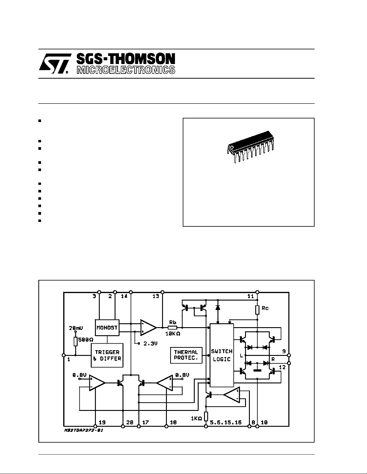
BLOCK DIAGRAM
Using the motor as a digital tachogenerator itself
the performance of true tacho controlled systems
isreached.
A dual loop control circuit provides long term stabilityand fast settling behaviour.
This is advanced information on a new product now in developmentor undergoing evaluation.Details aresubject to changewithout notice.
June 1992
1/16
TDA7272A
ABSOLUTE MAXIMUM RATINGS
Symbol Parameter Value Unit
V
S
V
S
I
O
P
tot
T
op
T
stg
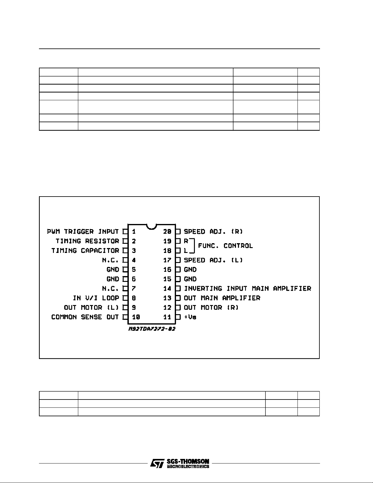
PIN CONNECTION (Topview)
DC Supply Voltage 24 V
Dump Voltage (300ms) 40 V
Output Current Internally limited
Power Dissipation at T
at T
pins
amb
=90°C
=70°C
4.3
1
Operating Temperature Range -40 to 85 °C
Storage Temperature -40 to 150 °C
W
W
THERMAL DATA
Symbol Parameter Value Unit
Thermal Resistance Junction-ambient max. 80 °C/W
Thermal Resistance Junction-pins max. 14 °C/W
2/16
R
th j-amb
R
th j-pins
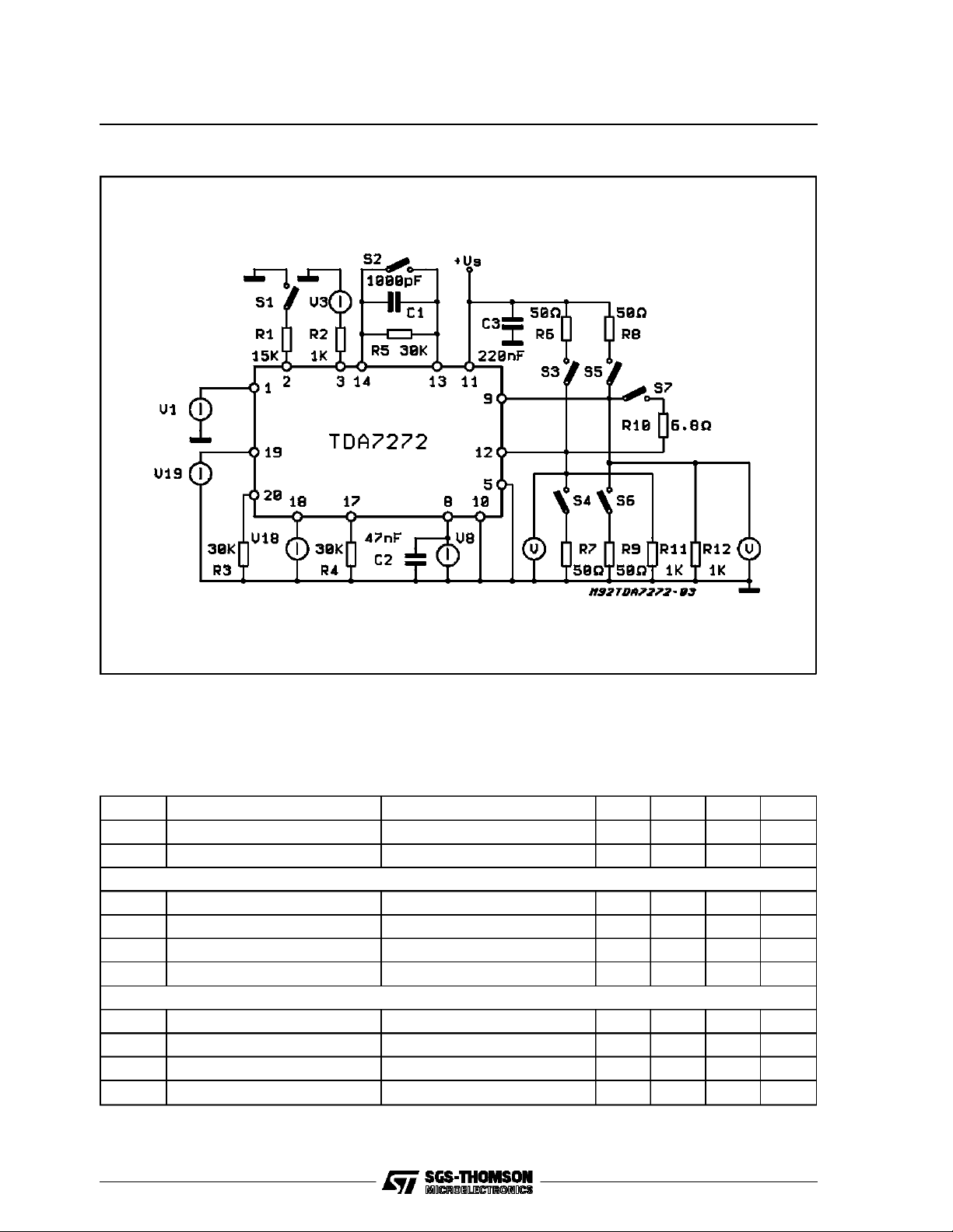
TEST CIRCUIT
TDA7272A
A
ELCTRICAL CHARACTERISTICS (T
=25°C; VS=13.5V unless otherwisespecified)
amb
Symbol Parameter Test Conditions Min. Typ. Max. Unit
V
I
Operating Supply Voltage 5.5 18 V
S
Supply Current No load 5 12 mA
S
OUTPUT STAGE
V
10,9,12
V
11,9,12
I
I
Output Currente Pulse 1 A
O
Output Currente Continuous 250 mA
O
Voltage Drop IO= 250mA 1.2 1.5 V
Voltage Drop IO= 250mA 1.7 2 V
MAIN AMPLIFIER
R
V
OFF
V
Input Resistance 100 KΩ
14
I
Bias Current 50 nA
b
Offset Voltage 1 5 mV
Reference Voltage Internal at non inverting input 2.3 V
R
3/16
TDA7272A
ELECTRICAL CHARACTERISTICS (Continued)
Symbol Parameter Test Conditions Min. Typ. Max. Unit
CURRENT SENSE AMPLIFIER
R
G
TRIGGER AND MONOSTABLE STAGE
V
R
V
T Low
V
V
V
2 REF
SPEED PROGRAMMING, DIRECTION CONTROL LOGICAND CURRENT SOURCE PROGRAMMING
V
18,19Low
V
18,19 High
I
18,19
V
17,20 REF
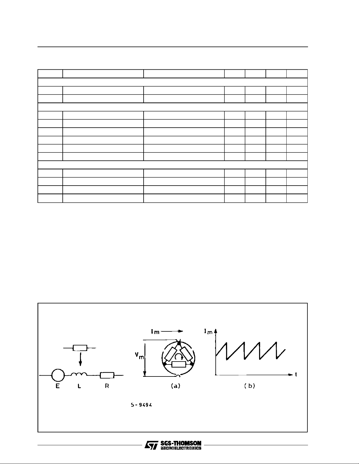
The TDA7272A novel applied solution is based
on a tachometer control system without using
such extra tachometer system. The information of
the actual motor speed is extracted from the motor itself. A DC motorwith an odd number of poles
generates a motor current which contains a fixed
number of discontinuities within each rotation. (6
for the 3 pole motor example on fig. 1)
Deriving this inherent speed information from the
motor current, it can be used as a replacement of
a low resolution AC tachometer system. Because
the settling time of the control loop is limited on
principleby the resolution in time of the tachome-
Figure1: Equivalent of a 3Pole DC Motor (a) and Typical motor CurrentWaveform (b).
Input Resistance 100 KΩ
8
Loop Gain 9
L
Input Allowed Voltage -0.7 3 V
IN1
Input Resistance 500 Ω
IN1
Trigger Level 0 V
Bias Voltage (pin 1) 15 20 25 mV
TB
Trigger Histeresis 10 mV
TH
Reference Voltage 750 800 850 mV
Input Low Level 0.7 V
Input High Level 2 V
Input Current 0 < V
Reference Voltage 735 800 865 mV
18,19<VS
2 µA
ter, this control principle offers a poor reaction
time for motors with a low number of poles. The
realized circuit is extended by a second feed forward loop in order to improve such system by a
fastauxiliary control path.
This additional path senses the mean output current and varies the output voltage according to
the voltage drop across the inner motor resistance. Apart from a current averaging filter, there
is no delay in such loop and a fast settling behaviour is reached in addition to the long term speed
motoraccuracy.
4/16
TDA7272A
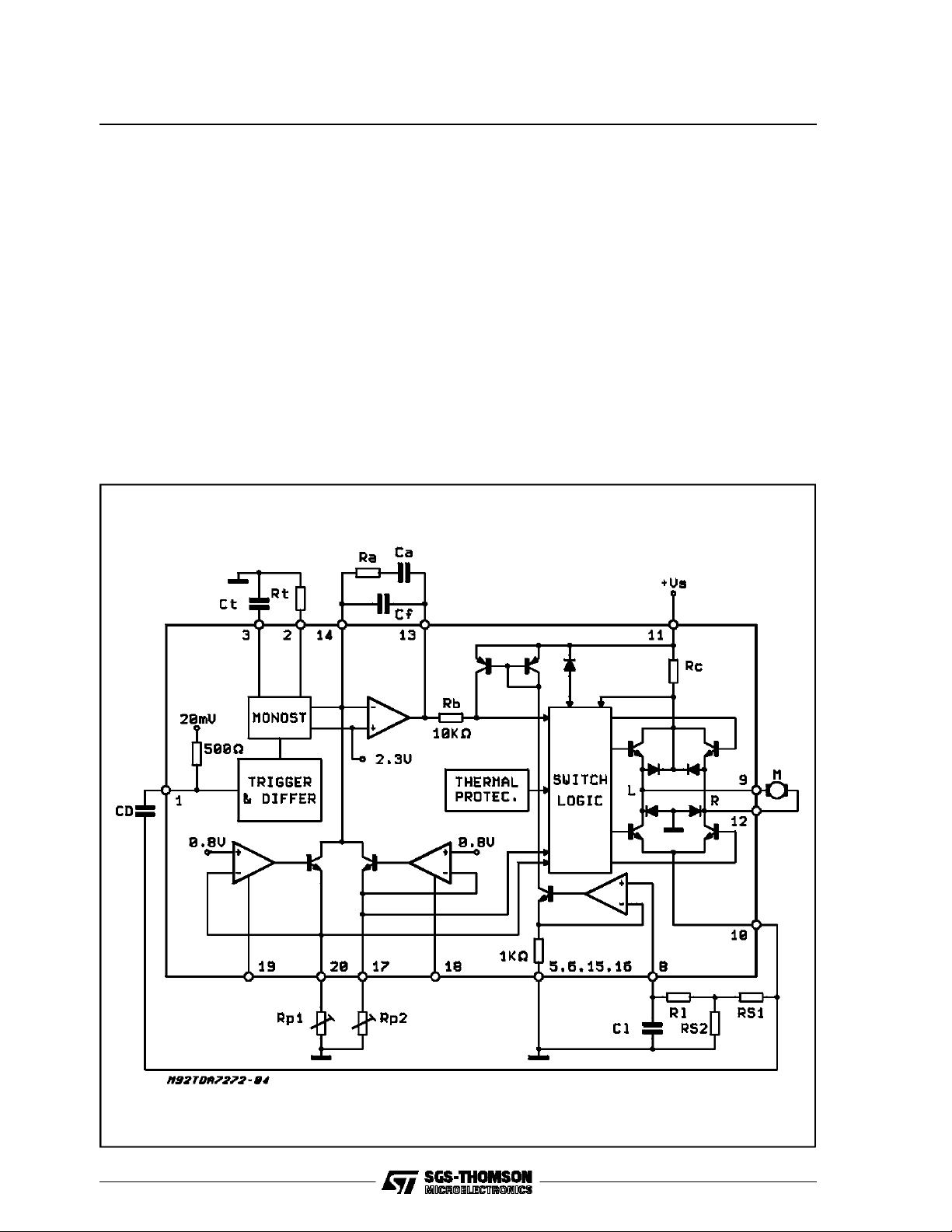
BLOCK DESCRIPTION
The principle structure of the element is shown in
fig. 2. As to be seen, the motor speed information
is derived from the motor current sense drop
across the resistors R
; capacitor CD together
S
with the input impedance of 500 Ω at pin 1 realizes a high pass filter.
This pin is internally biased at 20 mV, each negative zero transition switches the input comparator.
A 10 mV hysteresisimproves the noise immunity.
The trigger circuit is followed by an internal delay
time differentiator.
Thus, the system becomes widely independent of
the applied waveform at pin 1, the differentiator
triggers a monostable circuit which provides a
constant current duration. Both, output current
magnitude and duration T, are adjustable by ex-
Figure2: ApplicationCircuit.
ternalelements CT and RT.
The monostable is retriggerable ; this function
prevents the system from fault stabilization at
higherharmonics of the nominal frequency.
The speed programming current is generated by
two separate external adjustable current sources.
A corresponding digital input signal enables each
current source for left or right rotation direction.
ResistorRP1 and RP2 define the speed, the logicalinputs are at pin 18 and 19.
At the invertinginput (pin 14) of the main amplifier
the referencecurrent is compared with the pulsed
monostableoutput current.
For the correct motor speed, the reference current matches the mean value of the pulsed
monostable current. In this condition the charge
of the feedbackcapacitorbecomes constant.
5/16

TDA7272A
The speedn of a k pole motor results :
10.435
n =
C
TkRP
and becomes independent of the resistor RT
which only determines the current level and the
duty cycle which should be 1 : 1 at the nominal
speedfor minimumtorque ripple.
The second fast loop consists of a voltage to current converter which is driven at pin 8 by the low
pass filter R
. The output current at this stage
L,CL
is injected by a PNP current mirror into the inner
resistor R
. So the driving voltage of the output
B
stage consists of the integrator output voltage
plus the fastloop voltagecontribution across R
.
B
The power output stage realizes different modes
dependingon the logic status at pin 18 and19.
- Normal operation for left and right mode :
each upper TR of the bridge is used as
voltage follower whereas the lower acts as
a switch.
- Stop mode where the upper half is open
and the lower is conductive.
- High impedance status where all power
elementsare switched-off.
The high impedance status is also generated
when the supply voltage overcomes the 5 V to 20
V operating range or when the chip temperature
exceeds150 °C.
A short circuit protection limits the output current
at 1.5 A. Integrated diodes clamp spikes from the
inductiveload both at V
and ground.
CC
The reference voltages are derived from a common bandgap reference. All blocks are widely
suppliedby an internal 3.5 V regulator which providesa maximum supply voltage rejection.
Figure3.
Figure4.
PIN FUNCTION AND APPLICATION INFORMATION
PIN 1
Trigger input. Receives a proper voltage which
contains the information of the motor speed. The
waveform can be derived directly by the motor
current (fig. 3). The external resistor generates a
propervoltage drop. Togetherwith the input resistance at pin 1 [R
pacitorC
realizea high passfilter which differen-
D
(1) = 500 Ω ] the external ca-
IN
tiates the commutation spikes of the motor
current. Thetrigger level is 0V.
The biasing of the pin 1 is 20 mV with a hysteresis of 10 mV. So the sensing resistance must be
chosen high enough in order to obtain a negative
spike of the least 30 mV on pin 1, also with minimum variationof motor current :
S
∆I
MOT
min.
30mV
≥
R
Such value can be too much high for the preregulation stage V-I and it could be necessary to split
6/16
them into 2 series resistors R
=RS1+RS2(see
S
fig. 4) as explained on pin 8 section.
The information can be taken also from an exter-
nal tachogenerator.Fig. 5 shows various sources
connections:
the input signal mustn’t be lower than 0.7 V.

Figure5.
TDA7272A
Pin 2
Timing resistor. An internal reference voltage
(V2 = 0.8 V) gives possibility to fix by an external
resistor (R
), from this pin and ground, the output
T
current amplitudeof the monostable circuit, which
will be reflected into the timing capacitor (pin 3) ;
the typicalvalue would be about 50 µ A.
Figure6.
Pin 3
Timing capacitor. A constant current, determined
by the pin 2 resistor, flowing into a capacitor between pin 3 andground provides the output pulse
width of the monostable circuit, the max voltage
at pin 3 is fixed by an internal threshold : after
reaching this value the capacitor is rapidly dischargedand the pulsewidth is fixed to the value :
= 2.88 RTCT(fig.6)
T
on
Pin 4
Not connected.
Pin 5
Ground.Connected with pins6, 15, 16.
Pin 6
Ground.Connected with pins5, 15, 16.
Pin7
Notconnected.
Pin8
Input V/I loop. Receives from pin 10, through a
low pass filter, the voltage with the information of
the current flowing into the motor and produces a
negativeresistanceoutput :
R
= −9RS(fig. 7)
out
Figure7.
For compensating the motor resistance and
avoidinginstability:
R
MOTOR
≤
R
S
The optimization of the resistor R
9
for the tacho-
S
metric controlmust not give a voltage too high for
the V/I stage : one solutioncan be to divide in two
parts, as shown in fig.8, with :
R
M
=
R
S2
10
and R
+ RS2≥
S1
30mV
∆ I mot min.
(seepin 1 sect.)
The low pass filter R
must be calculated in
L,CL
order to reduce the ripple of the motor commutation at least 20 dB. Another example of possible
pins 10-8 connections is showed on fig. 9. A
choke can be used in order to reduce the radiation.
7/16

TDA7272A
Figure8.
Figure9.
substrate diodes, protect the output from inductive vol-tage spikes during the transition phase
(fig.10)
Figure10.
Pin10
Common sense output. From this pin the output
current of the bridge configuration (motor current)
is fed into R
external resistor in order to gener-
S
ate a propervoltagedrop.
The drop is supplied into pin 1 for tachometric
control andinto pin 8 for V/I control (see pin 1 and
pin 8 sections).
Pin 9
Output motor left. The four power transistors are
realized as darlington structures. The arrangement is controlled by the logic status at pins 18
and 19.
As beforeexplained (see block description), in the
normal left or right mode one of the lower darlington becomes saturated whereas the other remains open. The upper half of the bridge operates in the linear mode.
In stop condition both upper bridge darlingtons
are off and both lower are on. In the high output
impedance state the bridge is switched completelyoff.
Connecting the motor between pins 9 and 12
both left or right rotation can be obtained. If only
one rotation sense is used the motor can be connectedat only one output, byusing only the upper
bridge half. Two motors can be connected each
at the each output : in such case they will work alternatively(see application section).
The internal diodes, together with the collector
8/16
Pin11
Supplyvoltage.
Pin12
Outputmotor right. (seepin 9 section)
Pin13
Output main amplifier. The voltage on this pin results from the tachometric speed control and
feedsthe output stage.
The value of the capacitorC
(fig. 11), connected
F
from pins 13 and 14, must be chosen low enough
in order to obtain a short reaction time of the
tachometricloop, and high enough in order to reduce the output ripple.
A compromise is reached when the ripple voltage
(peak-to-peak)V
C
F
V
FEM
RIP
=
withV
cle = 50 %. (see pin 2-3 section)
is equal to 0.1 V
ROP
= 2.3
+ I
MOT
C
V
RIP
⋅ R
10
T
( 1 −
MOT
MOTOR
R
T
)
R
P
and with duty cy-
:

TDA7272A
Figure11.
Figure12.
Figure13.
In order to compensate the behaviour of the
whole system regulator-motor-load (considering
axis friction, load torque, inertias moment of the
motor of the load. etc.) a RC series network is
also connected between pins 13 and 14 (fig. 12).
The value of C
and RAmust been chosen ex-
A
perimentallyas follows:
- Increase of 10 % the speed with respect to
the nominal value by connecting in parallel
to R
a resistor with value about 10 time
p
larger.
- Vary the R
and CAvalues in order to ob-
A
tain at pin 13 a voltage signal with shortresponse time and without oscillations. Fig.
13 shows the step response at pin 13 versus R
andCAvalues.
A
Pin 14
9/16

TDA7272A
Figure14. Figure15.
Inverting input of main amplifier. In this pin the
current reference programmed at pins 20, 17 is
compared with the current from the monostable
(streamof rectangularpulses).
In steady-state condition (constant motor speed)
the values are equal and the capacitor C
voltage
F
is constant.
This means for the speed n (min 1):
10.435
=
n
C
TkRP
where ”k” is the number of collector segments.
(poles)
The non inverting input of the main amplifier is internallyconnected to a referencevoltage (2.3 V).
Pin 15
Ground.
Pin 16
Ground.
Pin 17
Left speed adjustment. The voltage at this pin is
fixed to a referencevalue of 0.8 V. A resistor from
this pin and ground (fig. 14) fixes the reference
current which will be compared with the medium
output current of the monostablein order to fix the
speed of the motor at the programmed value.The
correct value of R
would be :
p
10.435
=
R
P
C
kn
T
n = motor speed, (min -1)
k = poles number
The control of speed can be done in different
way:
- speed separately programmed in two
sensesofrotation (fig. 14-15) ;
- only one speed for the two senses of rotation (fig. 16) ;
Figure16.
Figure17.
- speeds of the two sensesa bit different(i.e.
for compensating different pulley effects)
(fig. 17) ;
- speed programmed with a DC voltage (fig.
18)i.e. with DA converter;
10/16

TDA7272A
- fast forward, by putting a resistor. In this
Figure19.
case it is necessary that also at the higher
speed for the duty cycle to be significately
less than 1 (see value of R
T,CT
on pin 2,
pin 3 sections).
Fig. 19 shows the functioncontrolled with a µP.
Figure18.
Thetypical value of the threshold (L-H) is 1.2 V.
Pin19
Left functioncontrol. (see pin 18 sect).
Pin 18
Right functioncontrol. The voltagesapplied to this
Pin20
Rightspeed adjustment. (seepin 17 sect).
pin and to pin 19 determine the function, as
showed in the table.
CONDITION
Pin 18 Pin 19 Pin 12 Pin 9
L
H
L
H
L
L
H
H
OUTPUT FUNCTION
STOP
LEFT
RIGHT
OPEN
OUTPUT VOLTAGE
LOW
LOW
REG
HIGH IMP.
HIGH IMP.
LOW
REG
LOW
Figure20: Typicalapplication.
11/16

TDA7272A
Figure21: Tachoonly speed regulation.
Figure22: One direction regulatorof one motor , or alternatively of two motors.
12/16

Figure23: P.C.board and componentslayout of the circuits of Figg. 20, 21, 22.
A
TDA7272A
APPLICATIONSUGGESTION (Fig.20,21,22) - (For a 2000 r.p.m. 3 pole DC motor with R
Components
R
S1
R
S2
R
L;CL
C
D
R
T;CT
R
P1;RP2
C
F
R
A;CA
Recommended
value
1Ω Current sensing
1.5Ω Current sensing
22KΩ - 68nF Spike filtering. Slow V/I
Purpose If larger If smaller
Tacho loop do
tacho loop.
V/I loop.
Instability may
occur.
not regulate
Motor regulator;
undercompens.
High output
regulator
ripple.
response.
68nF Pulse transf. 33nF 100nF
15KΩ - 47nF Current source
programming to
obtain a 50%
duty cycle
47KΩ trim. Set of speed. Low speed. High speed 0
Polyester 100nF Optimization of
integrator ripple
and loop
response time.
220KΩ - 220nF Fast response
with no
Lower ripple,
slower tacho
regulator
response.
Depending on electrmechanical
system.
Higher ripple,
faster response.
overshoot.
Allowed range
Min. Max.
67KΩ 30KW
10nF 470nF
10nF 470nF
=16Ω)
M
0
0R
MOT
/9
13/16

TDA7272A
Figure24: Speedregulation vs. supply voltage
(circuit of fig. 20).
Figure26: In connectionwitha PresettableCounter and I/O peripheralthe TDA7271A/TDA7272Acon-
trols the speedthrough a D/A Converter.
TDA7272A
14/16

POWERDIP 20 PACKAGEMECHANICAL DATA
TDA7272A
DIM.
MIN. TYP. MAX. MIN. TYP. MAX.
a1 0.51 0.020
B 0.85 1.40 0.033 0.055
b 0.50 0.020
b1 0.38 0.50 0.015 0.020
D 24.80 0.976
E 8.80 0.346
e 2.54 0.100
e3 22.86 0.900
F 7.10 0.280
I 5.10 0.201
L 3.30 0.130
Z 1.27 0.050
mm inch
15/16

TDA7272A
Information furnished is believed to be accurate and reliable. However, SGS-THOMSON Microelectronics assumes no responsibility for the
consequences of use of such information nor for any infringement of patents or other rights of third parties which may result from itsuse. No
license is granted by implication or otherwise under any patent or patent rights of SGS-THOMSON Microelectronics. Specifications mentioned in this publication are subject to change without notice. This publication supersedes and replaces all information previously supplied.
SGS-THOMSON Microelectronics products are not authorized for use as critical components in life support devices or systems without express written approval of SGS-THOMSON Microelectronics.
1994 SGS-THOMSON Microelectronics - All RightsReserved
SGS-THOMSON Microelectronics GROUP OF COMPANIES
Australia - Brazil- France - Germany - Hong Kong - Italy - Japan - Korea - Malaysia - Malta - Morocco - The Netherlands- Singapore -
Spain - Sweden - Switzerland - Taiwan - Thaliand- United Kingdom - U.S.A.
16/16
 Loading...