

2 x 2W STEREO AUDIO AMPLIFIER
WIDE OPERATING RANGE FROM 4.5V TO 18V
P
= 2W @ THD 10% 12V/8
OUT
INTERNAL FIXED GAIN 32dB
NO FEEDBACK CAPACITOR
NO BOUCHEROT CELL
THERMAL PROTECTION
AC SHORT CIRCUIT PROTECTION
SVR CAPACITOR FOR BETTER RIPPLE
REJECTION
LOW TURN-ON/OFF POP
VERY FEW EXTERNAL COMPONENTS
STAND -BY MODE (I
ST-BY
< 300µA)
DESCRIPTION
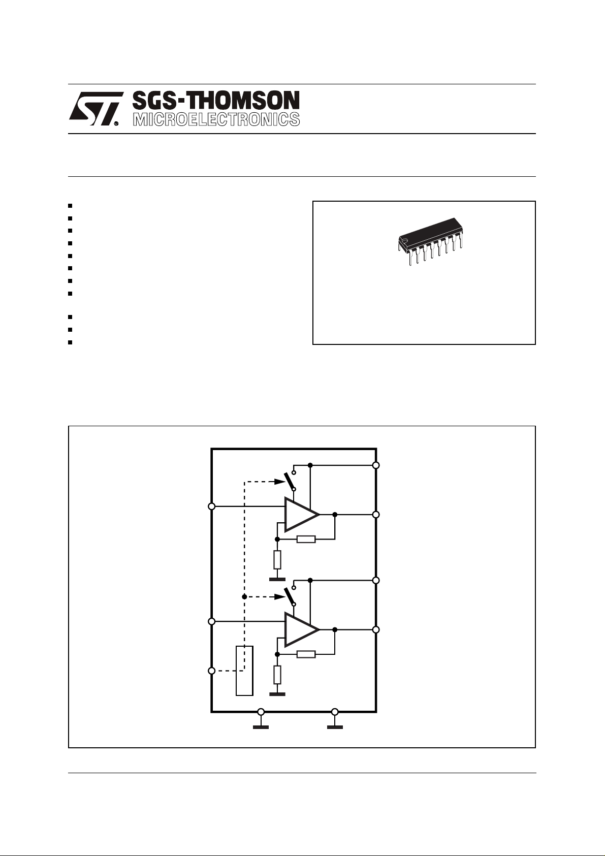
The device TDA7268 is a new technology stereo
Audio Amplifier in DIP package specially de-
BLOCK DIAGRAM
Ω
TDA7268
POWERDIP (8+8)
ORDERING NUMBER:
TDA7268
signed for TV application.
Thanks to the fully complementary output configu-
ration the device delivers a rail to rail voltage
swing without need of boostrap capacitor.
IN1
IN2
SVR
4
5
3
S-GND
+
-
+
-
69÷16
P-GND
1
2
8
7
V
S1
OUT1
V
S2
OUT2
D94AU167B
March 1998
1/5
TDA7268
ABSOLUTE MAXIMUM RATINGS
Symbol Parameter Value Unit
V
S
I
O
T
op
T
j
T
stg
PIN CONNECTION
Operating Supply Voltage 18 V
Output Peak Current 1.5 A
Operating Temperature Range 0 to 70 °C
Junction Temperature 150 °C
Storage Temperature Range -40 to 125 °C
V
S1
OUT1
SVR
IN1
IN2
S-GND
OUT2
V
S2
1
2
3
4
5
6
7
16
15
14
13
12
11
10
8 PGND9
D94AU164A
PGND
PGND
PGND
PGND
PGND
PGND
PGND
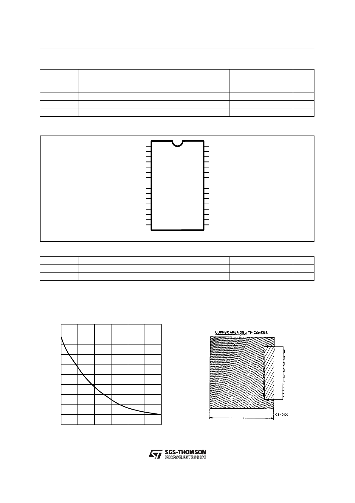
THERMAL DATA
Symbol Parameter Value Unit
R
th j-amb
R
th j-case
Rth with "on Board" Square Heat Sink vs. Copper
Thermal Resistance Junction to ambient (on PCB) Max. 70 °C/W
Thermal Resistance Junction to case Max. 15 °C/W
Example of heatsink using PC board copper
Area
54
52
50
48
46
44
42
40
38
36
34
THERMAL RESISTANCE JUNCTION TO AMBIENT(˚C/W)
024681012
ON BOARD HEAT-SINK AREA (sq.cm)
2/5
D98AU830

TDA7268
ELECTRICAL CHARACTERISTICS
= 25°C; VS = 12V; RL = 8Ω; f = 1KHz; unless ot herwise s pecified. )
(T
amb
Symbol Parameter Test Condition Min. Typ. Max. Unit
V
S
I
S
I
sb
V
O
A
V
∆A
R
IN
P
O
THD Distortion P
SVR Supply Voltage Rejection V
e
n
Supply Voltage Range 4.5 18 V
Quiescent Current 40 60 mA
Stand-By Current Pin 3 shorted to GND 0.15 0.3 mA
Quiescent Output Voltage 5.5 6 6.5 V
Voltage Gain 31 32 33 dB
Voltage Gain Matching 1.0 dB
V
Input Impedance 50 100 KΩ
Output Power THD = 10% 1.9 2 W
= 1W 0.1 0.4 %
O
= 150mVrms; F
rip.
R
= 10kΩ
S
R
= 50Ω 40
S
Total Input Noise Voltage Rg = 10KΩ; BW = 20Hz to
= 1KHz
rip.
50
46
48µV
20KHz
CT Cross Talk P
V
sb
A
sb
P
O
Stand-By Enable Voltage ISB < 300µA1V
Stand-By Attenution 60 80 dB
Output Power THD = 10%; VS = 9V; RL = 4Ω 1.8 W
= 1W; 50 60 dB
O
dB
dB
3/5

TDA7268
Fig. 1:
Standard Test and Application Circuit
C1 0.1µF
IN1
R1
10K
C2 0.1µF
IN2
R2
10K
S1
STAND-BY
Note: Add R1 & R2 on demoboard only for DC tests.
IN1
IN2
SVR
C3
47µF
4
5
3
69÷16
S-GND
+
-
+
-
P-GND
V
1
S1
100µF
OUT1
2
C5
470µF
V
8
S2
OUT2
7
C6 470µF
D94AU168D
C4
8Ω
8Ω
V
=12V
S
Fig. 2:
PCB And Components Layout Of The Application Circuit of Figure 1
APPLICATION HINTS:
For 12V supply and 8Ω speaker application, its
maximum power dissipation is about 2W.
Assumming that max ambient temperature is
70°C. Required thermal resistance of the device
and heat dissipating means must be equal to (150
- 70)/2 = 40°C/W.
Junction to pin thermal resistance of the package
is about 15°C/W.
That means external heat sink of about 25°C/W is
required. Stand-By switches must be able to discharge C
current.
svr
4/5

DIP16 PACKAGE MECHANICAL DATA
TDA7268
DIM.
MIN. TYP. MAX. MIN. TYP. MAX.
a1 0.51 0.020
B 0.77 1.65 0.030 0.065
b 0.5 0.020
b1 0.25 0.010
D 20 0.787
E 8.5 0.335
e 2.54 0.100
e3 17.78 0.700
F 7.1 0.280
I 5.1 0.201
L 3.3 0.130
Z 1.27 0.050
mm inch
5/5

TDA7268
Information furnis hed is believe d to be ac curate and reliabl e. However, SGS-THOMS ON Mi croelect ronics as sumes no res ponsib ility for the
consequences of use of such information nor for any infringement of patents or other rights of third parties w hi ch may result from i ts use. No
license is granted by implication or otherwise under any patent or patent rights of SGS-THOMSON Microelectronics. Specification mentioned
in this publication are subject to change without notice. This publication supersedes and replaces all information previously supplied.
SGS-THOMSON Microelectronics products are not authorized for use as critical components in life support devices or systems without express
written approval of SGS-THOMSON Microelectronics.
© 1998 SGS-THOMSON Microelectronics – Printed in Italy – All Rights Reserved
SGS-THOMSON Microelectronics GROUP OF COMPANIES
Australia - Brazil - Canada - China - France - Germany - Italy - Japan - Korea - Malaysia - Malta - Morocco - The Netherlands -
Singapore - Spain - Sweden - Switzerland - Taiwan - Thailand - United Kingdom - U.S.A.
6/5
 Loading...