


®
TDA7267A
3W MONO AMPLIFIER
CAN DELIVER 3W THD 10% 14.5V/8
Ω
INTERNAL FIXED GAIN 32dB
NO FEEDBACK CAPACITOR
NO BOUCHEROT CELL
THERMAL PROTECTION
AC SHORT CIRCUIT PROTECTION
SVR CAPACITOR FOR BETTER RIPPLE
REJECTION
LOW TURN-ON/OFF POP
STAND-BY MODE
DESCRIPTION
The device TDA7267A is a new technology Mono
Audio Amplifier in PowerDIP package specifically
designed for TV application.
Thanks to the fully complementary output configu-
BLOCK DIAGRAM
PowerDIP 8+8
ORDERING NUMBER:
TDA7267A
ration the device delivers a rail to rail voltage
swing without need of boostrap capacitors.
June 1998
IN
C3
47µF
C1 0.1µF
SVR
V
S
1
4
IN
3
6 9 to 16
S-GND P-GND
+
-
VS=14.5V
C4
100µF
C5 470µF
2
OUT
8Ω
D98AU827
1/7

TDA7267A
ABSOLUTE MAXIMUM RATINGS
Symbol Parameter Value Unit
V
S
I
O
T
op
T
j
T
stg
Operating Supply Voltage 18 V
Output Put Peak Current 1.5 A
Operating Temperature Range 0 to 70 °C
Junction Temperature 150 °C
Storage Temperature Range -40 to 125 °C
PIN CONNECTION
(Top view)
V
OUT
SVR
IN
N.C.
S-GND
N.C.
S
1
2
3
4
5
6
7 P-GND
N.C. 8 P-GND9
D98AU829
Rth with "on Board" Square Heat Sink vs. Copper
Area
54
52
50
48
46
44
42
40
38
36
34
THERMAL RESISTANCE JUNCTION TO AMBIENT(˚C/W)
024681012
ON BOARD HEAT-SINK AREA (sq.cm)
D98AU830
P-GND16
15
14
13
12
11
P-GND
P-GND
P-GND
P-GND
P-GND
10
Example of heatsink using PC board copper
2/7

TDA7267A
THERMAL DATA
Symbol Parameter Value Unit
R
th j-amb
R
th j-case
Thermal Resistance Junction to ambient 70 °C/W
Thermal Resistance Junction to case 15 °C/W
ELECTRICAL CHARACTERISTICS
= 25°C; VS = 14.5V; RL = 8Ω; f = 1KHz; unless otherwise
(T
amb
specified.)
Symbol Parameter Test Condition Min. Typ. Max. Unit
V
S
I
S
I
sb
V
O
A
V
R
IN
P
O
THD Distortion P
SVR Supply Voltage Rejection V
E
I
V
sb
Supply Voltage Range 5 18 V
Quiescent Current 23 35 mA
Stand-By Current Pin 3 shorted to GND 0.3 mA
Quiescent Output Voltage 7.5 V
Voltage Gain 31 33 dB
Input Impedance 50 100 KΩ
Output Power THD = 10% 2.7 3 W
= 1W 0.1 0.3 %
O
= 150mVrms;
ripple
F
= 1KHz
ripple
Input Noise Voltage Rg = 10KΩ; BW = 20Hz t o 2 0KHz 5 10 µV
Stand-By Enable Voltage 1 V
50 dB
Figure 1. Application Circuit
=14.5V
V
S
C1 0.1µF
IN
V
S
1
C4
100µF
C5 470µF
4
2
IN
OUT
SVR
8Ω
D98AU828
STAND-BY
C3
47µF
3
6
S-GND
9 to 16
P-GND
APPLICATION HINTS:
For 14.5V supply and 8Ω speaker application, its
maximum power dissipation is about 1.8W.
Assumming that max ambient temperature is
70°C, the required thermal resistance of the device mounted on t he PCB with a dissipating area
must be equal to: (150 - 70)/1.8 = 44.4°C/W.
Junction to pin thermal resistance of the package
is about 15°C/W. That means external heat sink
of about 30°C/W is required.
Cu ground plane of PCB can be used as heat dissipating means.
3/7
TDA7267A
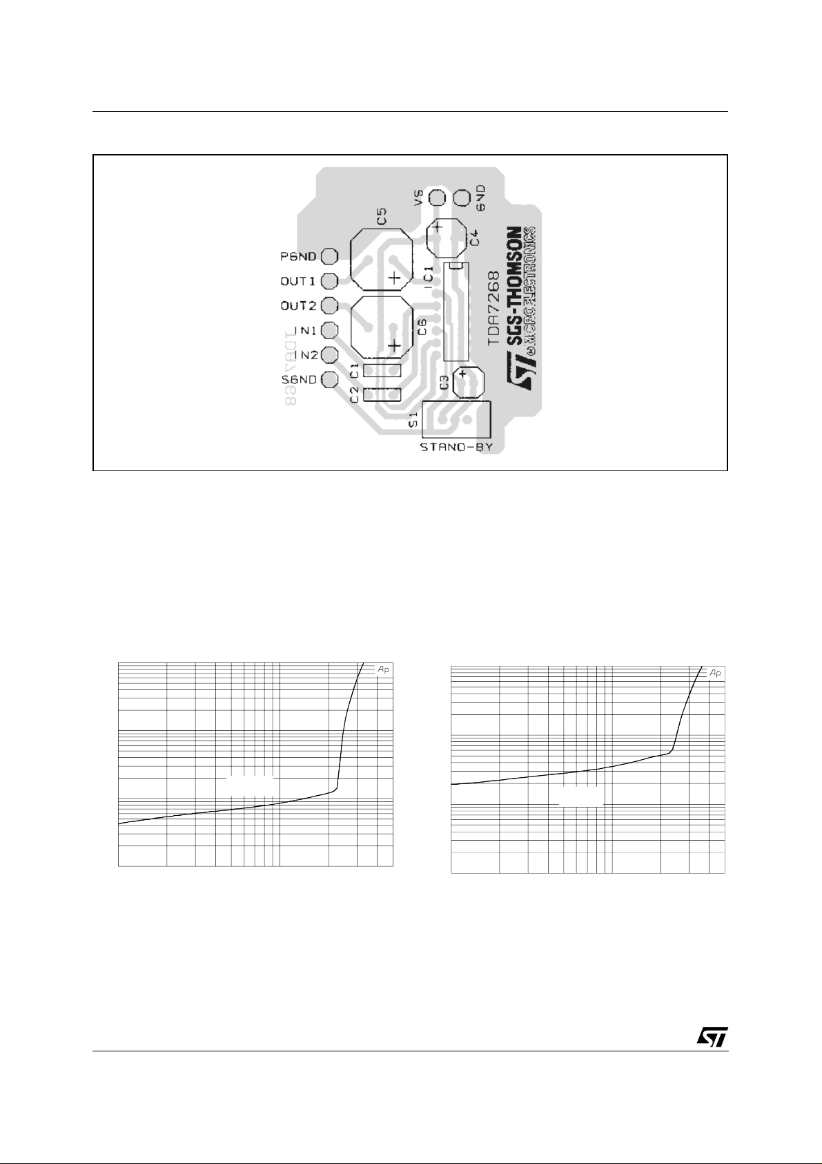
Figure 2. PCB And Components Layout Of The Application Circuit of Figure 1
Components C2 and C6 must be ignored.
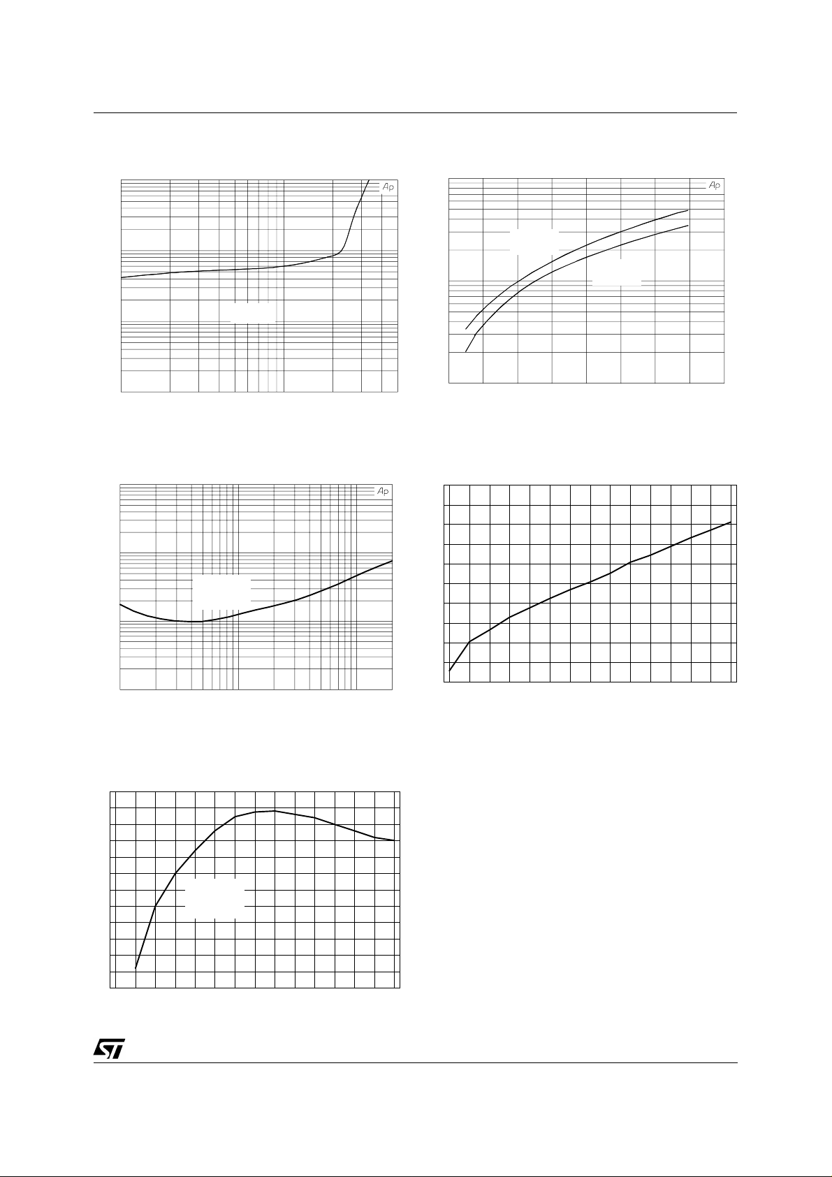
Figure 3. Distortion vs Output Power
THD+N(%)
10
1
0.1
0.010
0.1 1 5
Remark: all the characterization curves refer to the electrical test conditions.
f = 1KHz
Pout(W)
Figure 4. Distortion vs Output Power
THD+N(%)
10
1
0.1
0.010
0.1 1 5
f = 10KHz
Pout(W)
4/7
k
0
TDA7267A
Figure 5. Distortion vs Output Power
THD+N(%)
10
1
0.1
0.010
0.1 1 5
f = 15KHz
Pout(W)
Figure 7. Distortion vs Frequency
THD(%)
10
Figure 6. Output Power vs Supply Voltage
Pout (W)
10
f = 1KHz
THD=10%
f = 1KHz
1
0.1
4.000 6.000 8.000 10.00 12.00 14.00 16.00 18.00 20.00
THD= 1%
Vs(V)
Figure 8. Quiescent current vs Supply Voltage
Iq(mA)
30
25
1
Pout = 1W
Vs = 14.5V
Rl = 8 Ohm
0.1
0.010
100 1k 10k 20
f(Hz)
Figure 9. Power dissipation vs Output Power
Pd(W)
1.9
1.8
1.7
1.6
1.5
1.4
Vs = 14.5V
Rl = 8 Ohm
z
F = 1KH
20
15
10
5
456789101112131415161718
Vs(V)
1.3
0 0 .4 0.6 0.8 1.0 1.2 1.4 1.6 1.8 2.0 2.2 2.4 2.6 2.8 3.
Pout(W)
5/7
TDA7267A
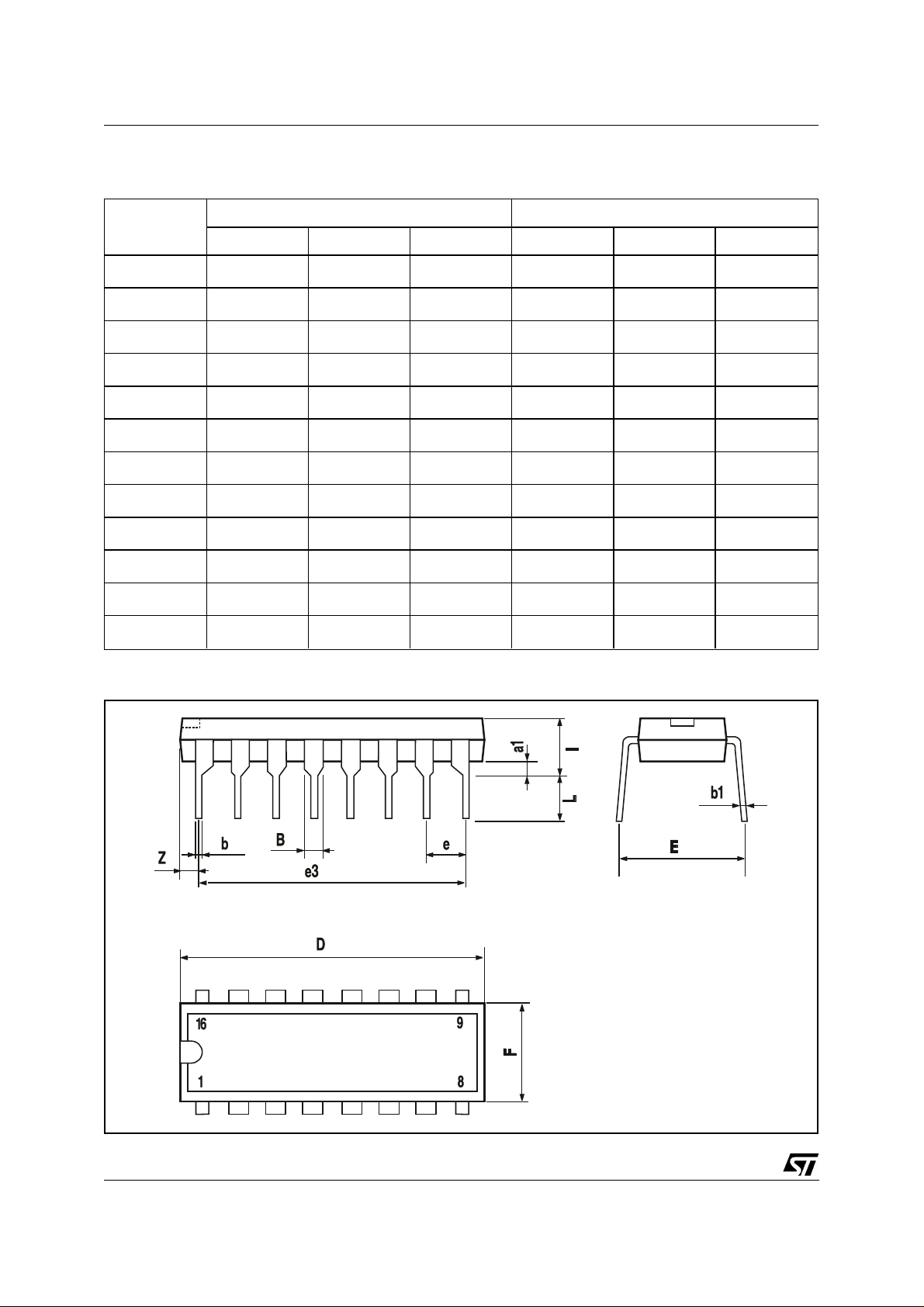
POWERDIP 8+8 PACKAGE MECHANICAL DATA
DIM.
MIN. TYP. MAX. MIN. TYP. MAX.
a1 0.51 0.020
B 0.77 1.65 0.030 0.065
b 0.5 0.020
b1 0.25 0.010
D 20 0.787
E 8.5 0.335
e 2.54 0.100
e3 17.78 0.700
F 7.1 0.280
I 5.1 0.201
L 3.3 0.130
Z 1.27 0.050
mm inch
6/7

TDA7267A
Information furnishe d is beli eved to be accu rate and reliable. However, STMicroelec tronics assumes no res ponsibility for the consequences
of use of such i nformation nor for any i nfringement of patents or ot her rights of third par ties which may result from its use. No license i s
granted by impli cation or otherwis e under any patent or patent righ ts of STMicroelect ronics. Specifica tion mentioned in this publication are
subject to change without notic e. This public ation supers edes and replaces all information prev iously supplied. STMic roelec tronic s products
are not authorized for use as critical components in life support devices or systems without express written approval of STMicroelectronics.
Australia - Brazil - Canada - China - France - Germany - Italy - Japan - Korea - Malaysia - Malta - Mexico - Morocco - The Netherlands -
Singapore - Spain - Sweden - Switzerland - Taiwan - Thailand - United Kingdom - U.S.A.
The ST logo is a registered trademark of STMicroelect roni cs
© 1998 STMicroelectronics – Printed in Italy – All Rights Reserved
STMicroelectronics GROUP OF COMPANIES
7/7
 Loading...