

TDA7266M
7W MONO BRIDGEAMPLIFIER
WIDESUPPLYVOLTAGERANGE(3-18V)
MINIMUMEXTERNALCOMPONENTS
– NOSWR CAPACITOR
– NOBOOTSTRAP
– NOBOUCHEROT CELLS
– INTERNALLYFIXED GAIN
STAND-BY & MUTEFUNCTIONS
SHORTCIRCUITPROTECTION
THERMALOVERLOADPROTECTION
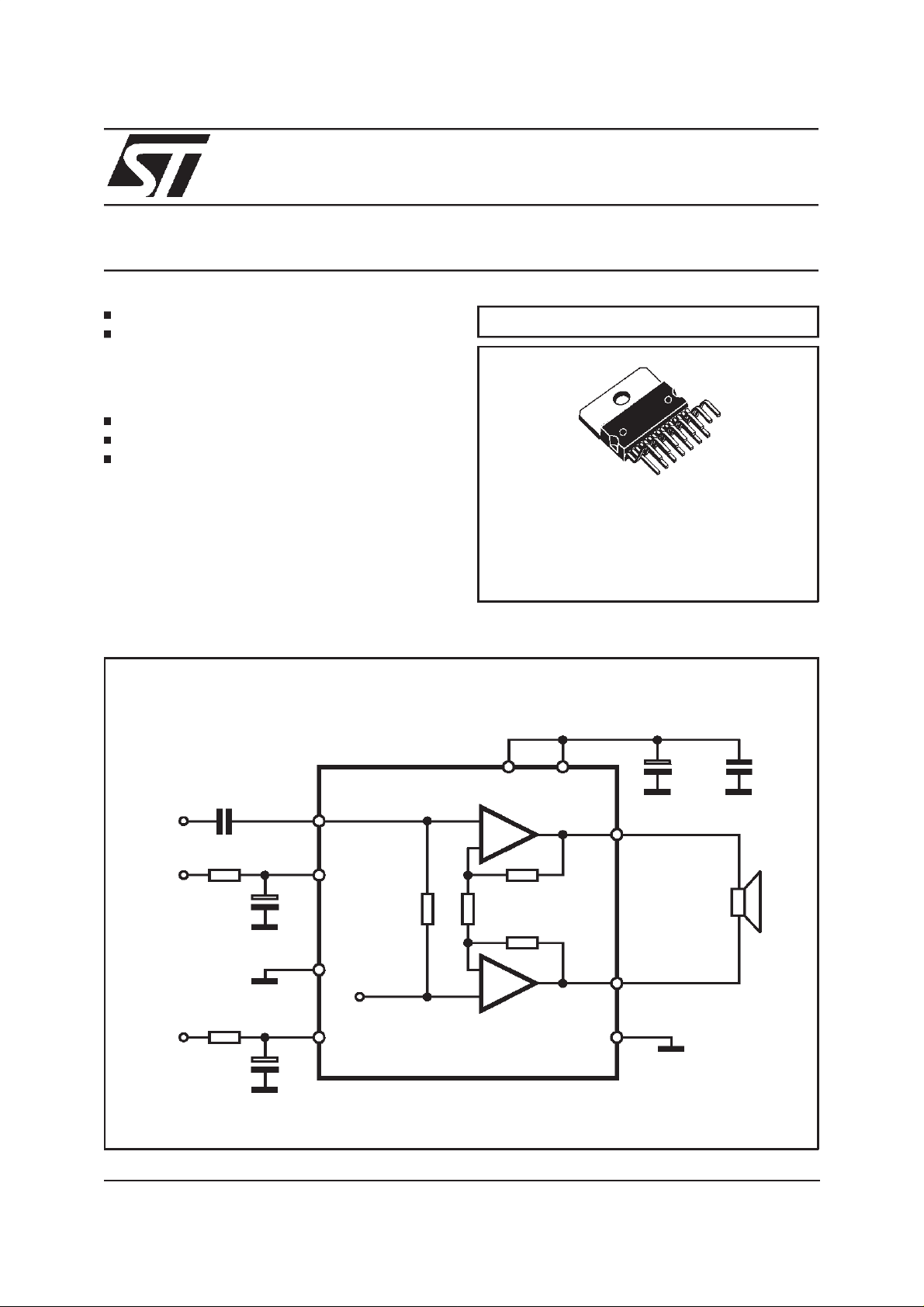
DESCRIPTION
The TDA7266M is a mono bridge amplifier specially designed for TV and Portable Radio applications.
BLOCK AND APPLICATIONDIAGRAM
TECHNOLOGY BI20II
Multiwatt 15
ORDERING NUMBER: TDA7266M
V
CC
0.22µF
IN1
ST-BY 7
S-GND
MUTE 6 8
August 1998
4
9
+
-
-
Vref
+
133
1
2
470µF 100nF
OUT1+
OUT1-
PW-GND
D98AU831A
1/9

TDA7266M
ABSOLUTE MAXIMUM RATINGS
Symbol Parameter Value Unit
V
I
P
T
T
stg,Tj
THERMAL DATA
Symbol Description Value Unit
R
th j-case
Supply Voltage 20 V
S
Output Peak Current(internally limited) 2 A
O
Total Power Dissipation (T
tot
Operating Temperature 0 to 70 °C
op
=70°C) 33 W
case
Storage and Junction Temperature -40 to +150 °C
Thermal Resistance Junction to case Typ. 1.4 Max. 2 °C/W
PIN CONNECTION
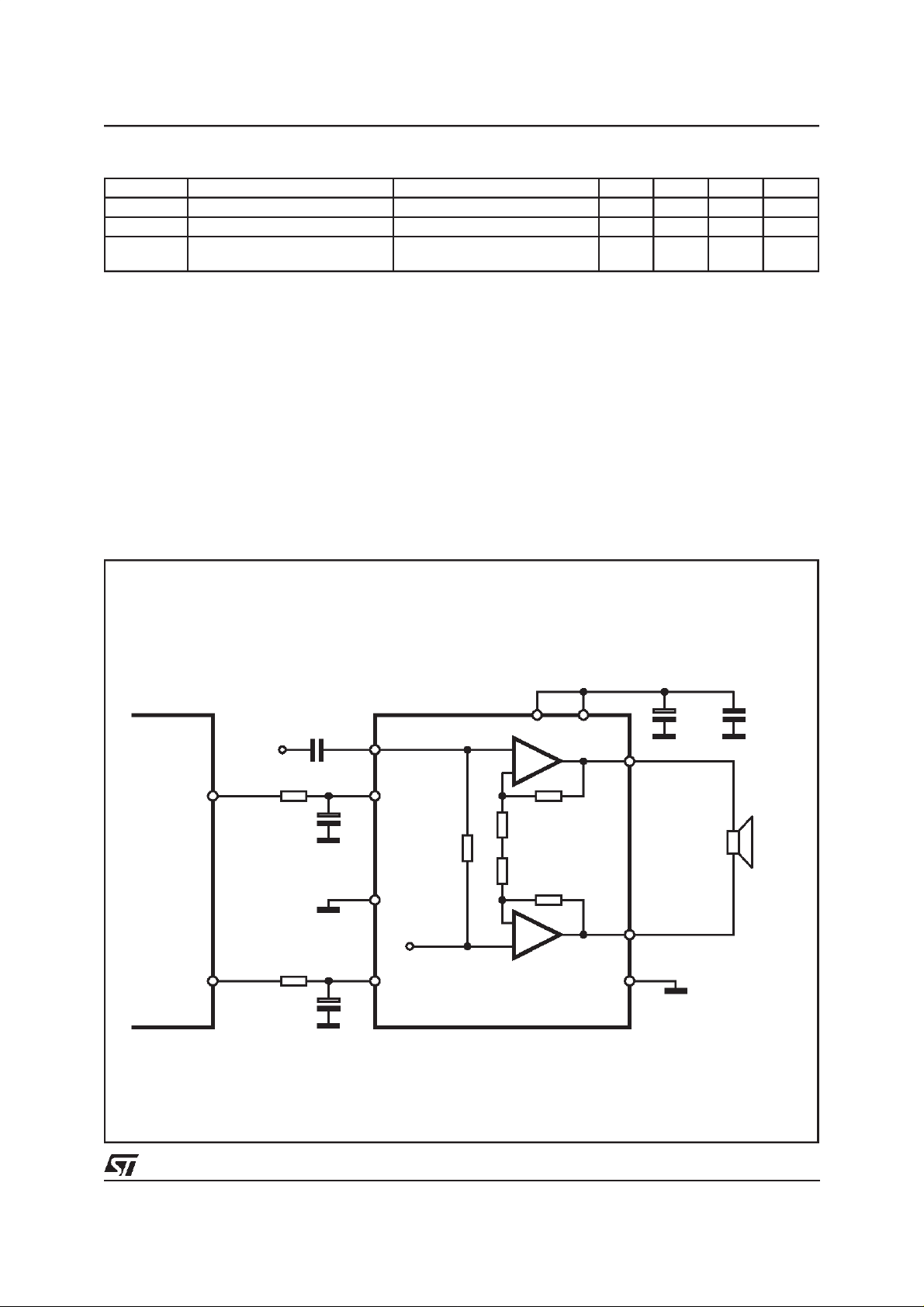
ELECTRICAL CHARACTERISTICS
(Top view)
15
14
13
12
11
10
9
8
7
6
5
4
3
2
1
= 11V, RL=8Ω, f = 1kHz, T
(V
CC
D98AU832
N.C.
N.C.
VCC
N.C.
N.C.
N.C.
S-GND
PW-GND
ST-BY
MUTE
N.C.
IN1
V
CC
OUT1OUT1+
=25°C unless otherwise
amb
specified.)
Symbol Parameter Test Condition Min. Typ. Max. Unit
V
CC
I
q
V
OS
P
O
THD Total Harmonic Distortion P
SVR Supply Voltage Rejection f = 100Hz VR = 0.5V 40 56 dB
A
MUTE
T
W
G
V
R
VT
MUTE
Supply Range 3 11 18 V
Total Quiescent Current 50 65 mA
Output Offset Voltage 120 mV
Output Power THD = 10% 6.3 7 W
= 1W 0.05 0.2 %
O
P
= 0.1W to 2W
O
f = 100Hz to 15kHz
Mute Attenuation 60 80 dB
Thermal Threshold 150
Closed LoopVoltage Gain 25 26 27 dB
Input Resistance 25 30 KΩ
i
Mute Threshold for VCC> 6.4V; VO= -30dB
for V
< 6.4V; VO= -30dB
CC
2.3
VCC/2
-1
2.9
V
CC
-0.75
/2
1%
4.1
V
/2
CC
-0.5
C
°
V
V
2/9
TDA7266M
ELECTRICALCHARACTERISTICS
Symbol Parameter Test Condition Min. Typ. Max. Unit
VT
ST-BY
I
ST-BY
e
N
St-by Threshold 0.8 1.3 1.8 V
ST-BY current V6 = GND 100 µA
Total Output Noise Voltage A curve
APPLICATIONSUGGESTION
STAND-BYAND MUTE FUNCTIONS
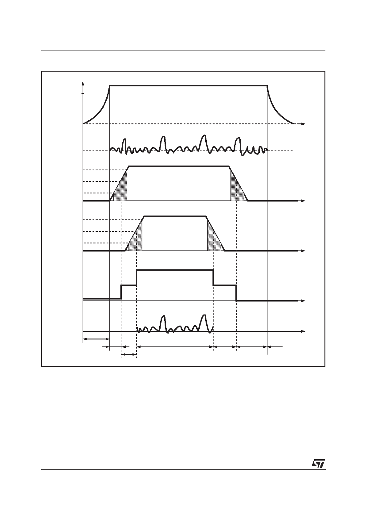
(A) MicroprocessorApplication
In order to avoid annoying ”Pop-Noise” during
Turn-On/Off transients, it is necessary to guarantee the right St-by and mute signals sequence.
It is quite simple to obtain this function using a microprocessor(Fig.1 and 2).
At first St-by signal (from mP) goes high and the
voltage across the St-by terminal (Pin 7) startsto
increase exponentially. The external RC network
is intended to turn-onslowly the biasing circuits of
(Continued)
150
f = 20Hz to 20kHz
the amplifier, this to avoid ”POP” and ”CLICK” on
the outputs.
When this voltage reaches the St-by threshold
level, the amplifier is switched-onand the external
capacitors in series to the input terminals (C3,
C5) start to charge.
It’s necessaryto mantain the mute signal low until
the capacitors are fully charged, this to avoid that
the device goes in play mode causing a loud”Pop
Noise”on the speakers.
A delay of 100-200ms between St-by and mute
signals is suitable for a properoperation.
Figure 1: MicroprocessorApplication
V
µ
µP
IN1
ST-BY
MUTE
C1 0.22µF
R1 10K
C2
10µF
R2 10K
C4
1µF
S-GND
V
CC
4
7
9
Vref
68
+
-
-
+
133
1
OUT1+
2
OUT1-
PW-GND
C5
470µF
D98AU833A
C6
100nF
3/9
TDA7266M
Figure 2:
MicroprocessorDriving Signals.
+VS(V)
+18
V
IN
(mV)
V
ST-BY
pin 7
1.8
1.3
0.8
V
MUTE
pin 6
4.1
2.9
2.3
I
q
(mA)
V
OUT
(V)
OFF
ST-BY
MUTE
PLAY MUTE ST-BY
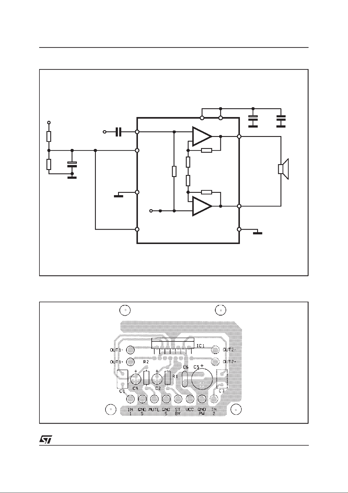
(B) Low Cost Application
In low cost applications where the mP is not present, the suggestedcircuit is shown in fig.3.
The St-by and mute terminals are tied together
and they are connected to the supply line via an
OFF
D96AU259
externalvoltage divider.
The device is switched-on/off from the supply line
and the external capacitor C4 is intendedto delay
the St-by and mute threshold exceeding, avoiding
”Popping”problems.
4/9
TDA7266M
Figure 3a:
IN1
R1
47K
R2
47K
Stand-aloneLow-cost Application.
C3 0.22µF
IN1
ST-BY
C4
10µF
S-GND
MUTE
4
7
9
Vref
68
V
CC
133
+
1
470µF
OUT1+
C1
C2
100nF
-
-
2
OUT1-
+
PW-GND
Figure 3b:
DASHED PARTS
ARE NOT TO BE
CONSIDERED
D98AU834A
PCB and ComponentLayout of the Application Circuit (Fig. 1).
5/9

TDA7266M
Figure 4:
THD(%)
10
DistortionvsOutputPower
Vcc =11 V
Rl = 8 ohm
1
f = 15 KHz
0.1
f = 5 KHz
f = 1 KHz
0.010
0.1 1 10
Pout (W)
Figure 6:
THD(%)
0.010
DistortionvsFrequency
10
Vcc= 11V
1
0.1
Rl = 8ohm
Pout= 100mW
Pout= 2W
100 1k 10k 20k
frequency (Hz)
Figure5:
THD(%)
0.010
Distortionvs Output Power
10
Vcc = 9V
Rl= 8 ohm
1
f = 15KHz
0.1
f = 5 KHz
f = 1KHz
0.1 1 10
Pout (W)
Figure7:
Level(dBr)
5.0000
4.0000
3.0000
2.0000
1.0000
0.0
-1.000
-2.000
-3.000
-4.000
-5.000
Gainvs Frequency
Vcc = 11V
Rl= 8ohm
Pout = 1W
10 100 1k 10k 100k
frequency(Hz)
Figure 8: OutputPower vs. Supply Voltage
Po(W)
20.000
18.000
16.000
14.000
12.000
10.000
8.0000
6.0000
4.0000
2.0000
0.0
2.000 4.000 6.000 8.000 10.00 12.00 14.00 16.00 18.00
6/9
Rl = 8 ohm
f = 1KHz
d=10%
d=1%
Vs(V)
Figure9: Total Power Dissipation& Efficiency
vs. Output Power
Pd (W)
4
3.5
3
2.5
2
1.5
1
0.5
0
Pd
µ
Vcc = 11V
Rl = 8ohm
f = 1KHz
00.511.522.533.544.555.566.577.58
Pout(W)
(%)
µ
80
70
60
50
40
30
20
10
0

TDA7266M
Figure 10:
MuteAttenuationvs. V pin.6
Attenua tio n(dB )
10
0
-10
-20
-30
-40
-50
-60
-70
-80
-90
-100
11.522.533.544.55
Vpin.6(V)
Figure 12:
QuiescentCurrent vs. Supply Voltage
Iq(mA)
70
65
60
55
Figure11:
Attenuation (dB)
10
0
-10
-20
-30
-40
-50
-60
-70
-80
-90
-100
-110
-120
0 0.2 0.4 0.6 0.8 1 1.2 1.4 1.6 1.8 2 2.2 2.4
Stand-ByAttenuationvs Vpin.7
Vp in.7(V)
50
45
40
35
30
3456789101112131415161718
Vsuppl y(V)
7/9

TDA7266M
MULTIWATT15 PACKAGE MECHANICAL DATA
DIM.
A 5 0.197
B 2.65 0.104
C 1.6 0.063
D 1 0.039
E 0.49 0.55 0.019 0.022
F 0.66 0.75 0.026 0.030
G 1.02 1.27 1.52 0.040 0.050 0.060
G1 17.53 17.78 18.03 0.690 0.700 0.710
H1 19.6 0.772
H2 20.2 0.795
L 21.9 22.2 22.5 0.862 0.874 0.886
L1 21.7 22.1 22.5 0.854 0.870 0.886
L2 17.65 18.1 0.695 0.713
L3 17.25 17.5 17.75 0.679 0.689 0.699
L4 10.3 10.7 10.9 0.406 0.421 0.429
L7 2.65 2.9 0.104 0.114
M 4.25 4.55 4.85 0.167 0.179 0.191
M1 4.63 5.08 5.53 0.182 0.200 0.218
S 1.9 2.6 0.075 0.102
S1 1.9 2.6 0.075 0.102
Dia1 3.65 3.85 0.144 0.152
MIN. TYP. MAX. MIN. TYP. MAX.
mm inch
8/9

TDA7266M
Information furnished is believed to be accurate and reliable. However, STMicroelectronics assumes no responsibility for the consequences
of use of such information nor for any infringement of patents or other rights of third parties which may result from its use. No license is
granted by implication or otherwise under any patent or patent rights of STMicroelectronics. Specification mentioned in this publication are
subject to change without notice. This publication supersedes and replaces all information previously supplied. STMicroelectronics products
are not authorized for use as criticalcomponents in lifesupport devices or systems without express written approval ofSTMicroelectronics.
The ST logo is a registeredtrademarkof STMicroelectronics
1998 STMicroelectronics– Printed in Italy – AllRights Reserved
STMicroelectronics GROUP OF COMPANIES
Australia - Brazil - Canada - China- France - Germany - Italy - Japan - Korea- Malaysia - Malta - Mexico - Morocco - The Netherlands -
Singapore - Spain - Sweden - Switzerland- Taiwan - Thailand- United Kingdom - U.S.A.
9/9
 Loading...