

TDA7264
25 + 25W STEREO AMPLIFIER WITH MUTE/ST-BY
WIDE SUPPLY VOLTAGE RANGE (UP TO
50V ABSMAX.)
SPLIT SUPPLY
HIGHOUTPUTPOWER:
25 + 25W @ THD =10%, R
NO POPAT TURN-ON/OFF
MUTE(POP FREE)
STAND-BY FEATURE (LOWI
FEWEXTERNALCOMPONENTS
SHORTCIRCUITPROTECTION
THERMALOVERLOAD PROTECTION
DESCRIPTION
The TDA7264/TDA7264A is class AB dual Audio
power amplifier assembled in the Multiwatt package, speciallydesigned for high quality sound ap-
=8Ω,VS= +20V
L
Q)
TDA7264A
Multiwatt 8 Multiwatt 11
ORDERING NUMBER: TDA7264 (Multiwatt 8)
TDA7264A (Multiwatt 11)
plication as Hi-Fi music centers and stereo TV
sets.
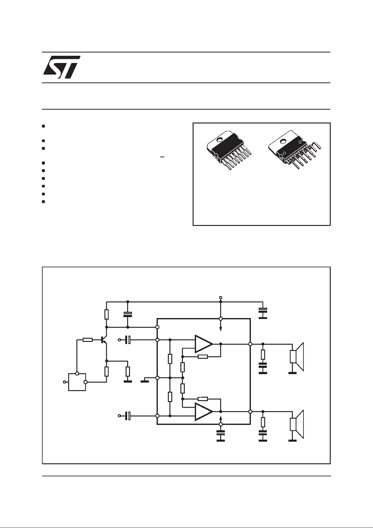
Figure 1: Typical ApplicationCircuit for TDA7264
+5V
15K 1µF
µP
1µF
1µF
MUTE/
ST-BY
IN (L)
18K15K
GND
IN (R)
D94AU069A
4
6
7
8
-
-
+
1000µF
+V
S
OUT (L)
4.7Ω
OUT (R)
4.7Ω
1000µF
RL (L)
100nF
RL (R)
100nF
+V
2
5
-V
S
3+
1
S
April 1999
1/12
TDA7264 - TDA7264A
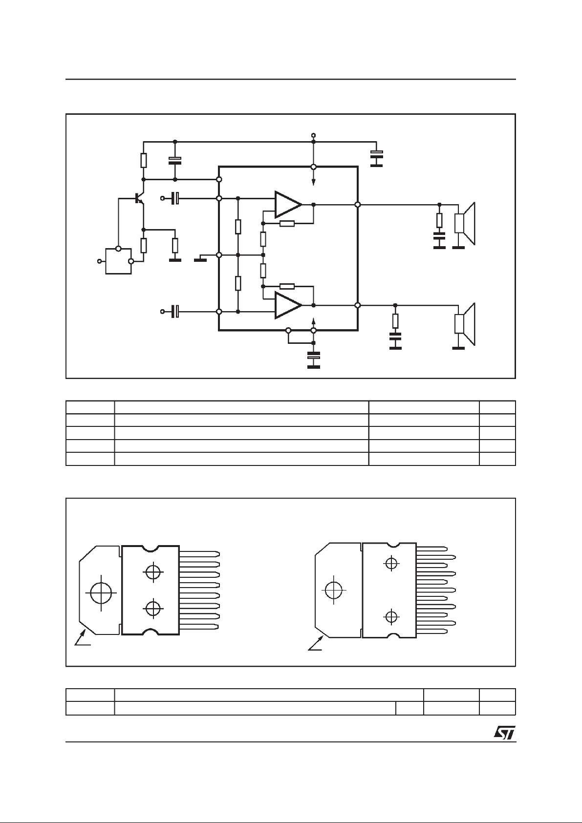
Figure 2: Typical ApplicationCircuit for TDA7264A
+V
S
1000µF
OUT (L)
4.7Ω
100nF
OUT (R)
4.7Ω
100nF
+5V
15K 1µF
µP
1µF
1µF
MUTE/
ST-BY
IN (L)
18K15K
GND
IN (R)
D98AU955
5
7
9
11
-
-
+
1
1000µF
3
4+
2
6
-V
S
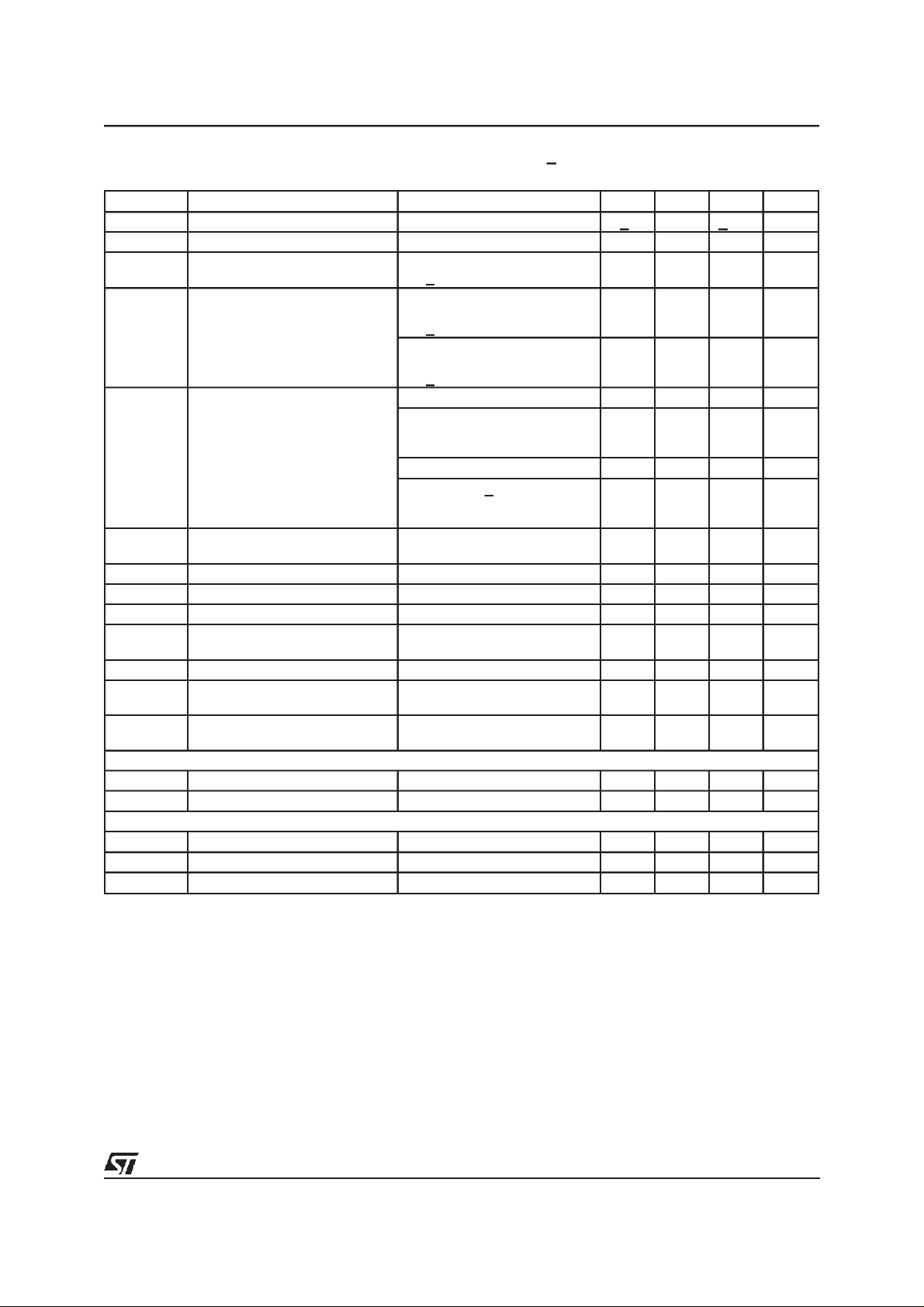
ABSOLUTE MAXIMUM RATINGS
Symbol Parameter Value Unit
V
I
O
P
tot
T
stg,Tj
DC Supply Voltage 50 V
S
Output Peak Current (internally limited) 4.5 A
Power Dissipation T
=70°C30W
case
Storage and Junction Temperature -40 to +150 °C
RL (L)
RL (R)
PIN CONNECTION (Topview)
Tab connected to pin 5
Multiwatt 8
8 IN (1)
7
6
5
4
3
2
1
D94AU096
GND
IN (2)
-V
S
MUTE/ST-BY
OUTPUT (2)
+V
S
OUTPUT (1)
TAB CONNECTEDTOPIN 6
Multiwatt 11
11
10
9
8
7
6
5
4
3
2
1
D98AU956
IN(1)
NOT CONNECTED
GND
NOT CONNECTED
IN(2)
-V
S
STBY/MUTE
OUTPUT(2)
+V
S
OUTPUT(1)
-V
S
THERMAL DATA
Symbol Description Value Unit
Thermal Resistance Junction-case Max 2
2/12
R
th j-case
C/W
°
TDA7264 - TDA7264A
ELECTRICALCHARACTERISTICS (Refer to the test circuit, VS+ 20V; RL=8Ω;Rs=50Ω;
f = 1KHz; T
Symbol Parameter Test Condition Min. Typ. Max. Unit
V
S
I
q
P
O
P
O
THD Total Harmonic Distortion R
C
T
SR Slew Rate 10 V/µs
G
V
∆G
V
e
N
R
i
SVR Supply Voltage Rejection
T
j
MUTE FUNCTION [ref: +V
VT
MUTE
A
M
STAND-BY FUNCTION [ref:+V
VT
ST-BY
A
ST-BY
I
q ST-BY
Note :
(*) FULL POWER up to.V
MUSIC POWER is the maximal power which the amplifier is capable of producing across theratedloadresistance (regardless of non linearity)
1 sec after the application of a sinusoidal input signal of frequency 1KHz.
=25°C, unless otherwise specified.)
amb
Supply Range +5 +22.5 V
Total Quiescent Current 80 130 mA
Music Output Power (*) THD = 10%; RL=8Ω ;
V
+ 22.5V
S
32 W
Output Power THD = 10%
R
=8Ω ;
L
V
+ 16V; RL=4
S
Ω
20 25
25
THD = 1%
R
=8Ω ;
L
V
+ 16V; RL=4
S
=8Ω ;PO= 1W; f = 1KHz 0.02 %
L
=8Ω ;
R
L
P
= 0.1 to 15W;
O
Ω
20
20
0.5 %
f = 100Hz to 15KHz
R
=4Ω;PO= 1W; f = 1KHz 0.03 %
L
=4Ω ;VS+ 16V;
R
L
P
= 0.1 to 12W;
O
1%
f = 100Hz to 15KHz
Cross Talk f = 1KHz
f = 10KHz
70
60
Closed Loop Voltage Gain 29 30 31 dB
Voltage Gain Matching 0.2 dB
Total Input Noise A Curve
f = 20Hz to 22KHz
2.5
3.5 8
Input Resistance 15 20 KΩ
fr = 100Hz; Vripple= 0.5V
RMS
60 dB
(each channel)
Thermal Shut-down
145
Junction Temperature
S]
Mute / PlayThreshold -7 -6 -5 V
Mute Attenuation 60 90 dB
]
S
Stand-by / Mute Threshold -3.5 -2.5 -1.5 V
Stand-by Attenuation 110 dB
Quiescent Current@ Stand-by 3 mA
=±22.5V with RL=8Ωand VS= ±16V with RL=4Ω
S
W
W
W
W
dB
dB
µV
µ
°
V
C
3/12
TDA7264 - TDA7264A
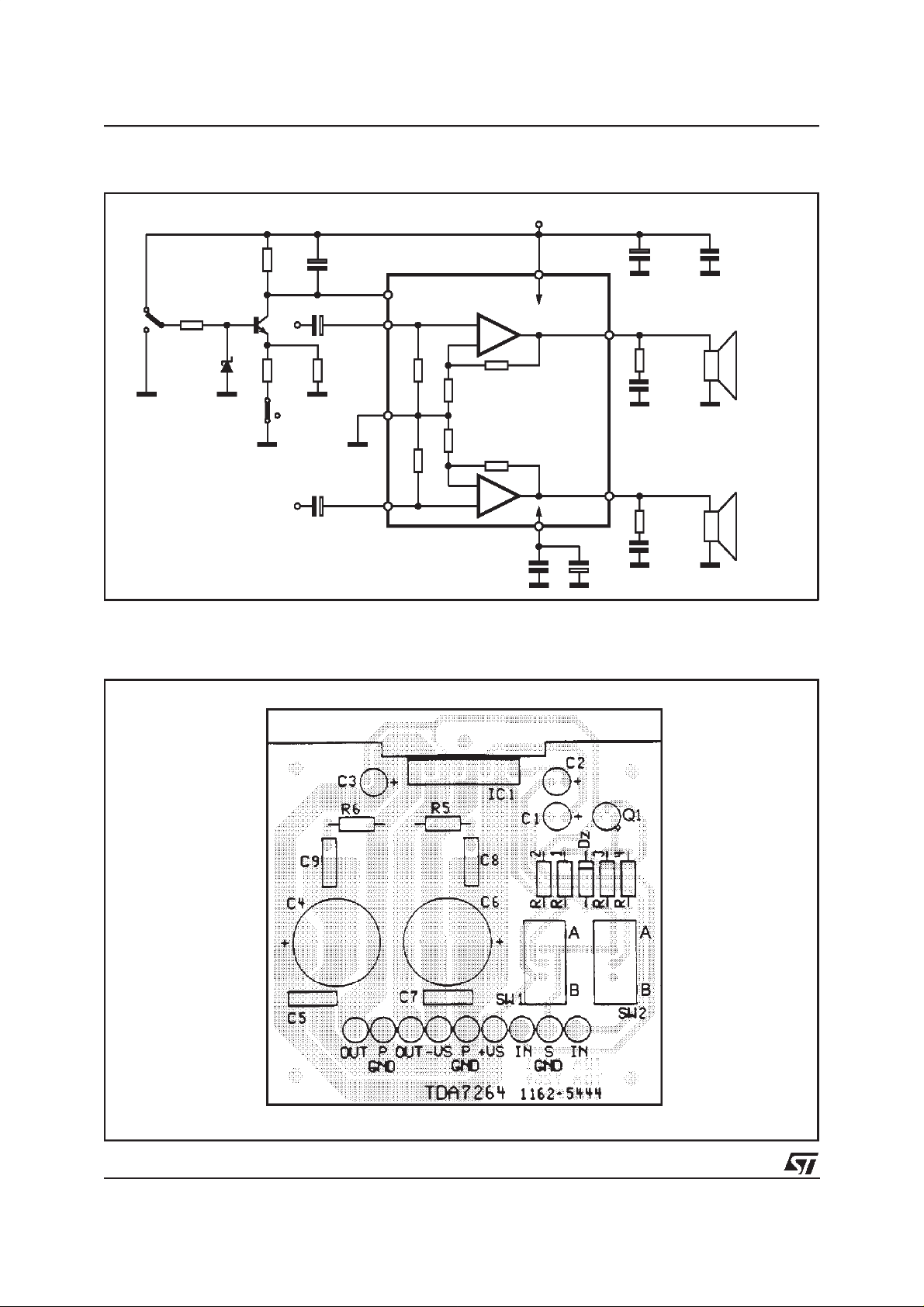
Figure 3: Demo Board Schematic TDA7264
R2
C3
1µF
R4
15K
SW2
MUTE
C1 1µF
MUTE/
ST-BY
IN (L)
R3
18K
GND
SW1
ST-BY
R1
15K
Q1
DZ
+V
S
+V
S
4
6
-
7
2
3+
C4
1000µF
OUT (L)
R5
4.7Ω
C8
100nF
C5
100nF
RL (L)
C2 1µF
IN (R)
D94AU068B
8
-
+
C7
100nF
1
OUT (R)
5
-V
S
C6
1000µF
R6
4.7Ω
100nF
RL (R)
C9
Figure 3a: P.C.Board And ComponentLayout of the Demo Board Schematic TDA7264 (1:1 Scale)
4/12

Figure 4: Demo Board Schematic TDA7264A
+V
TDA7264 - TDA7264A
S
SW1
ST-BY
R1
DZ
SW2
MUTE
R2 C3
Q1
R4
R3
C1
C2
MUTE/
ST-BY
IN (L)
GND
IN (R)
D98AU957
+V
S
C7
3
4+
2
6
-V
S
C6
5
7
-
9
11
-
+
1
C4
OUT (L)
OUT (R)
R10
C9
C5
R7
C8
RL (L)
RL (R)
Figure 4a: P.C.Board And ComponentLayout of the Demo Board Schematic TDA7264A (1:1 Scale)
TDA7264A
5/12

TDA7264 - TDA7264A
APPLICATIONS SUGGESTIONfor TDA7264
(Demo Board Schematic)
The recommended values of the external compo-
COMPONENTS
R1 10KΩ Mute Circuit
R2 15KΩ Mute Circuit V
R3 18KΩ Mute Circuit V
R4 15KΩ Mute Circuit V
R5, R6 4.7Ω Frequency Stability Danger of Oscillations Danger of Oscillations
C1, C2 1µF
C3 1µF
C4, C6 1000µF
C5, C7 0.1µF
C8, C9 0.1µF Frequency Stability
Dz 5.1V Mute Circuit
Q1 BC107 Mute Circuit
RECOMMENDED
VALUE
PURPOSE
Input DC
Decoupling
St-By/Mute Time
Constant
Supply Voltage
Bypass
Supply Voltage
Bypass
APPLICATIONS SUGGESTIONfor TDA7264A
(Demo Board Schematic)
The recommended values of the external compo-
COMPONENTS
R1 10K
R2 15KΩ Mute Circuit V
R3 18KΩ Mute Circuit V
R4 15KΩ Mute Circuit V
R7, R10 4.7Ω Frequency Stability Danger of Oscillations Danger of Oscillations
C1, C2 1µF
C3 1µF
C4, C6 1000µF
C5, C7 0.1µF
C8, C9 0.1µF Frequency Stability
Dz 5.1V Mute Circuit
Q1 BC107 Mute Circuit
RECOMMENDED
VALUE
Ω
PURPOSE
Mute Circuit
Input DC
Decoupling
St-By/Mute Time
Constant
Supply Voltage
Bypass
Supply Voltage
Bypass
nents are those shown on the demo board schematic. Different values can be used: the following
table can help the designer.
LARGER THAN
RECOMMENDED VALUE
Increase of Dz
Biasing Current
pin # 4 Shifted Downward Vpin # 4 Shifted Upward
pin # 4 Shifted Upward Vpin # 4 Shifted Downward
pin # 4 Shifted Upward Vpin # 4 Shifted Downward
Larger On/Off Time Smaller On/OffTime
SMALLER THAN
RECOMMENDED VALUE
Higher Low Frequency
Cutoff
Danger of Oscillations
Danger of Oscillations
nents are those shown are the demo board schematic different values can be used: the following
table can help the designer.
LARGER THAN
RECOMMENDED VALUE
Increase of Dz
Biasing Current
pin # 5 Shifted Downward Vpin # 5 Shifted Upward
pin # 5 Shifted Upward Vpin # 5 Shifted Downward
pin # 5 Shifted Upward Vpin # 5 Shifted Downward
Larger On/Off Time Smaller On/OffTime
SMALLER THAN
RECOMMENDED VALUE
Higher Low Frequency
Cutoff
Danger of Oscillations
Danger of Oscillations
MUTE, STAND-BY TRUTH TABLE
SW1 SW2
A A STAND-BY
A B STAND-BY
B B MUTE
B A PLAY
6/12

TDA7264 - TDA7264A
Figure 5: QuiescentCurrent vs. Supply Voltage Figure6: FrequencyResponse
Figure 7: OutputPower vs SupplyVoltage
Figure8: Distortionvs. OutputPower
Figure 9: Crosstalkvs. Frequency Figure10: SupplyVoltageRejection vs.Fequency
7/12
TDA7264 - TDA7264A
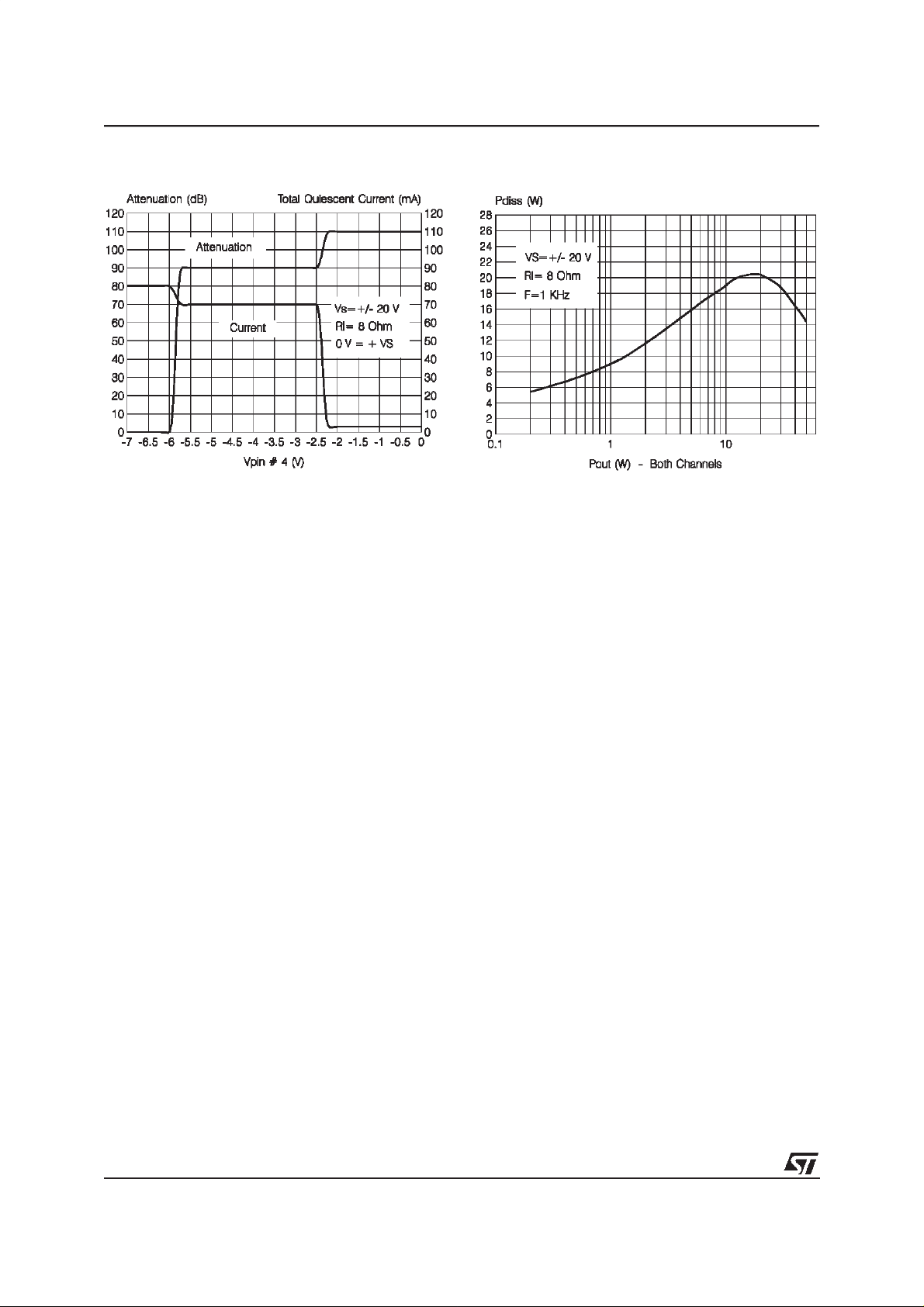
Figure 11: Attenuation& Total QuiescentCur-
rent vs. V
pin4
Voltage
Figure12: Power Dissipation vs. Output Power
8/12

TDA7264 - TDA7264A
MUTE STAND-BY FUNCTION
The pin 4 (MUTE/STAND-BY) controls the amplifier status by two different thresholds, referred to
.
+V
S
- When V
higher than = +VS- 2.5V the
pin4
amplifier is in Stand-by mode and the final
stage generatorsare off
Figure 13
+V
S
(V)
20
-V
S
-20
V
IN
(mV)
- when V
is between +VS- 2.5V and +V
pin4
- 6V the final stage current generators are
switched on and the amplifier is in mute
mode
- when V
is lower than +VS- 6V the am-
pin4
plifier is play mode.
t
S
Vpin4
(V)
V
S
VS-2.5
VS-6
VS-10
I
q
(mA)
0
VOUT
(V)
STDBY
OFF
PLAY STDBY PLAY OFF
STDBY
MUTE MUTE
D94AU084
MUTE
MUTE
9/12
TDA7264 - TDA7264A
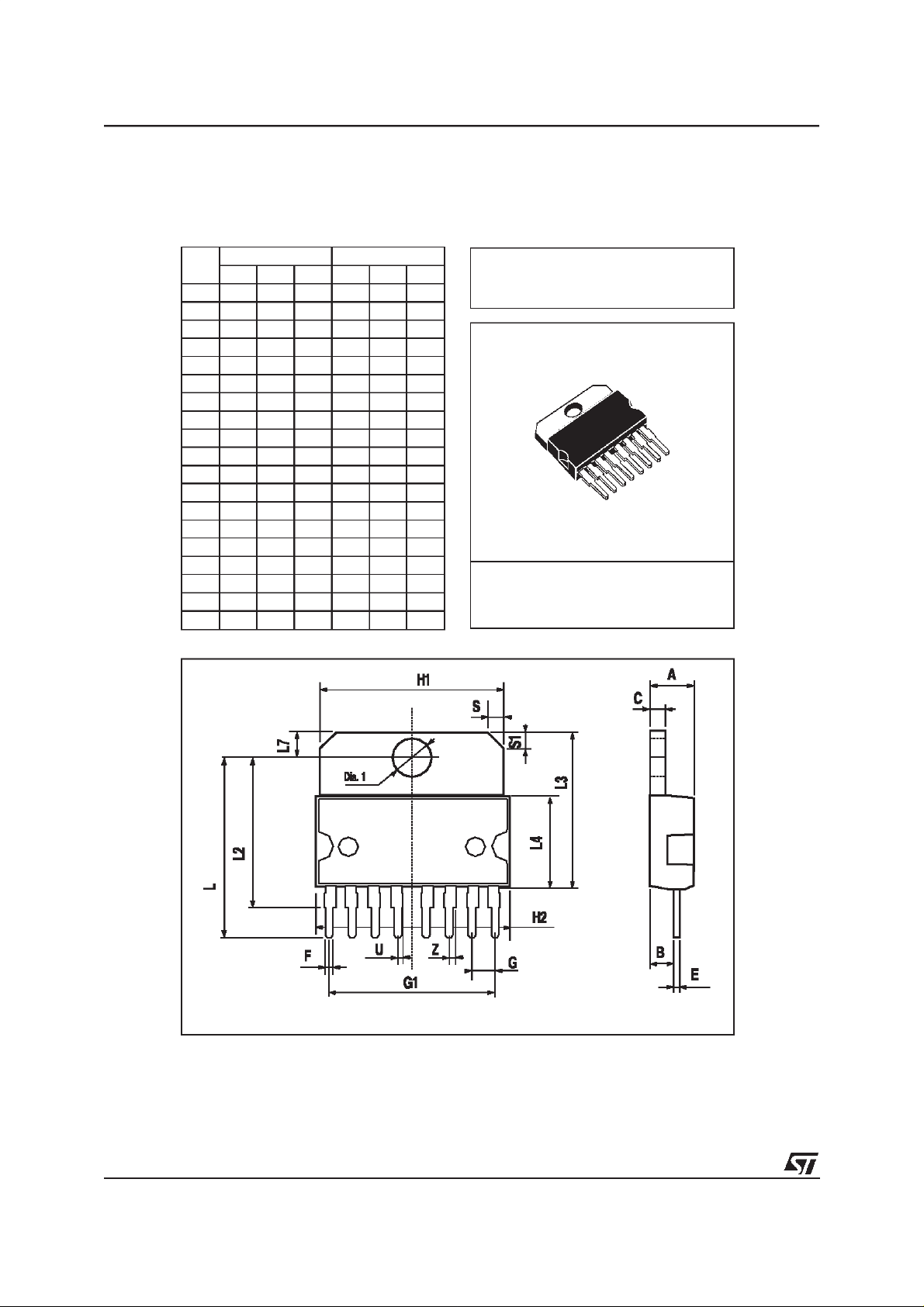
DIM.
A 5 0.197
B 2.65 0.104
C 1.6 0.063
E 0.49 0.55 0.019 0.022
F 0.78 0.85 0.030 0.033
G 2.40 2.54 2.68 0.094 0.10 0.105
G1 17.64 17.78 17.92 0.69 0.70 0.71
H1 19.6 0.772
H2 20.2 0.795
L 20.35 20.65 0.80 0.81
L2 17.05 17.20 17.35 0.67 0.68 0.68
L3 17.25 17.5 17.75 0.679 0.689 0.699
L4 10.3 10.7 10.9 0.406 0.421 0.429
L7 2.65 2.9 0.104 0.114
S 1.9 2.6 0.075 0.102
S1 1.9 2.6 0.075 0.102
U 0.40 0.55 0.015 0.022
Z 0.70 0.85 0.028 0.034
Dia1 3.65 3.85 0.144 0.152
mm inch
MIN. TYP. MAX. MIN. TYP. MAX.
OUTLINE AND
MECHANICALDATA
Multiwatt8 (Pin. 5 Gnd)
10/12

TDA7264 - TDA7264A
DIM.
MIN. TYP. MAX. MIN. TYP. MAX.
A5
B 2.65 0.104
C 1.6 0.063
D 1 0.039
E 0.49 0.55 0.019 0.022
F 0.88 0.95 0.035 0.037
G 1.45 1.7 1.95 0.057 0.067 0.077
G1 16.75 17 17.25 0.659 0.669 0.679
H1 19.6 0.772
H2 20.2 0.795
L 21.9 22.2 22.5 0.862 0.874 0.886
L1 21.7 22.1 22.5 0.854 0.87
L2 17.4 18.1 0.685
L3 17.25 17.5 17.75 0.679 0.689 0.699
L4 10.3 10.7 10.9 0.406 0.421 0.429
L7 2.65 2.9 0.104 0.114
M 4.25 4.55 4.85 0.167 0.179 0.191
M1 4.73 5.08 5.43 0.186 0.200 0.214
S 1.9 2.6 0.075 0.102
S1 1.9 2.6 0.075 0.102
Dia1 3.65 3.85 0.144 0.152
mm inch
0.197
0.886
0.713
OUTLINE AND
MECHANICAL DATA
Multiwatt11 V
11/12

TDA7264 - TDA7264A
Information furnished is believed to be accurate and reliable. However, STMicroelectronics assumes no responsibility for the consequences
of use of such information nor for any infringement of patents or other rights of third parties which may result from its use. No license is
granted by implication or otherwise under any patent or patent rights of STMicroelectronics. Specification mentioned in this publication are
subject to change without notice. This publication supersedes and replaces all information previously supplied. STMicroelectronics products
are not authorized for use as critical components in life support devices or systems without express written approval of STMicroelectronics.
Australia - Brazil - Canada - China - France - Germany - Italy - Japan - Korea - Malaysia - Malta - Mexico - Morocco - The Netherlands -
Singapore - Spain - Sweden - Switzerland- Taiwan - Thailand - United Kingdom - U.S.A.
The ST logo is a registered trademark of STMicroelectronics
1999 STMicroelectronics – Printed in Italy – All Rights Reserved
STMicroelectronics GROUP OF COMPANIES
http://www.st.com
12/12
 Loading...