


25W MONO AMPLIFIER WITHMUTE/ST-BY
WIDE SUPPLY VOLTAGE RANGE (UP TO
50V ABSMAX.)
SPLIT SUPPLY
HIGHOUTPUT POWER:
25W @ THD =10%,R
NO POPAT TURN-ON/OFF
MUTE(POP FREE)
STAND-BY FEATURE (LOWI
FEWEXTERNAL COMPONENTS
SHORTCIRCUIT PROTECTION
THERMALOVERLOAD PROTECTION
DESCRIPTION
The TDA7261 is class AB Audio power amplifier
assembled in the Multiwatt package, specially de-
Figure 1: Typical Application Circuit
=8Ω,VS= +20V
L
Q)
TDA7261
Multiwatt 8
ORDERING NUMBER: TDA7261
signed for high quality sound application in mono
TV chassis.
+5V
February 1997
µP
15K 1µF
1µF
MUTE/
ST-BY
18K15K
D94AU088
IN
GND
+V
S
OUT
1000µF
4.7Ω
100nF
RL
1/9
+V
S
4
6
-
7
1000µF
2
3+
5
-V
S

TDA7261
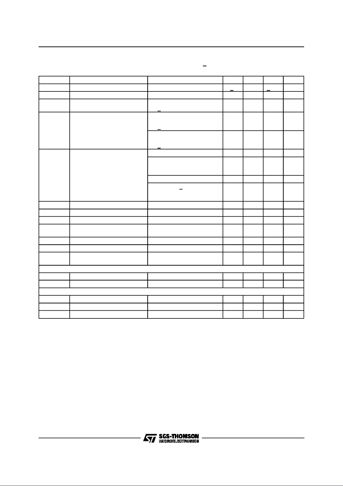
ABSOLUTE MAXIMUM RATINGS
Symbol Parameter Value Unit
V
I
O
P
tot
T
stg,Tj
PIN CONNECTION(Topview)
DC Supply Voltage 50 V
S
Output PeakCurrent (internally limited) 4.5 A
Power Dissipation T
Storage and Junction Temperature -40 to +150 °C
=70°C30W
case
8 N.C.
7
6
5
4
3
2
1
GND
IN
-V
S
MUTE/ST-BY
OUTPUT
+V
S
N.C.
Tab connected to pin 5
D94AU090
THERMAL DATA
Symbol Description Value Unit
R
th j-case
Thermal Resistance Junction-case Max 2.5 °C/W
2/9
TDA7261
ELECTRICALCHARACTERISTICS (Referto the test circuit,VS+ 20V; RL=8Ω;Rs=50Ω;
f = 1KHz; T
Symbol Parameter Test Condition Min. Typ. Max. Unit
V
S
I
q
P
O
P
O
THD Total Harmonic Distortion R
SR Slew Rate 10 V/µs
G
V
∆G
V
e
N
R
i
SVR Supply Voltage Rejection fr = 100Hz; Vripple = 0.5V
T
j
MUTE FUNCTION [ref: +V
VT
MUTE
A
M
STAND-BY FUNCTION [ref: +V
VT
ST-BY
A
ST-BY
I
q ST-BY
Note :
(*) FULL POWER up to.V
MUSICPOWER is themaximal powerwhich theamplifier is capableof producing across therated load resistance(regardless of non linearity)
1 sec after the application of a sinusoidal input signal of frequency 1KHz.
=25°C, unlessotherwise specified.)
amb
Supply Range +5 +22.5 V
Total Quiescent Current 30 mA
Music Output Power (*) THD = 10%; RL=8Ω ;
V
+ 28.5V;
S
32 W
Output Power THD = 10%
R
=8Ω ;
L
V
+ 16V; RL=4
S
Ω
20 25
25
THD = 1%
R
=8Ω ;
L
V
+ 16V; RL=4
S
=8Ω ;PO= 1W; f= 1KHz 0.02 %
L
=8Ω ;
R
L
P
= 0.1 to 15W;
O
Ω
20
20
0.5 %
f = 100Hz to 15KHz
R
=4Ω;PO= 1W; f =1KHz 0.03 %
L
=4Ω ;VS+ 16V;
R
L
P
= 0.1 to 12W;
O
1%
f = 100Hz to 15KHz
Closed Loop Voltage Gain 29 30 31 dB
Voltage Gain Matching 0.2 dB
Total Input Noise A Curve
f = 20Hz to 22KHz
2.5
3.5 8
Input Resistance 15 20 KΩ
RMS
Thermal Shut-down
60 dB
145
Junction Temperature
S]
Mute / PlayThreshold -7 -6 -5 V
Mute Attenuation 60 90 dB
]
S
Stand-by / Mute Threshold -3.5 -2.5 -1.5 V
Stand-by Attenuation 110 dB
Quiescent Current @ Stand-by 3 mA
=±22.5V with RL=8Ωand VS= ±16V with RL=4Ω
S
W
W
W
W
µV
µV
°
C
3/9

TDA7261
APPLICATIONS SUGGESTION
(Demo BoardSchematic)
The recommendedvalues of the external compo-
COMPONENTS
R1 10KΩ Mute Circuit
R2 15KΩ Mute Circuit V
R3 18KΩ Mute Circuit V
R4 15KΩ Mute Circuit V
R5 4.7Ω Frequency Stability Danger of Oscillations Danger of Oscillations
C1 1µF
C2 1µF
C3, C5 1000µF
C4, C6 0.1µF
RECOMMENDED
VALUE
PURPOSE
Input DC
Decoupling
St-By/Mute Time
Constant
Supply Voltage
Bypass
Supply Voltage
Bypass
nents are those shown on the demo board schematic. Different values can be used: the following
table can help the designer.
LARGER THAN
RECOMMENDED VALUE
Increase of Dz
Biasing Current
# 4 Shifted Downward V
pin
# 4 Shifted Upward V
pin
# 4 Shifted Upward V
pin
Larger On/Off Time Smaller On/Of Time
SMALLER THAN
RECOMMENDED VALUE
# 4 ShiftedUpward
pin
# 4 ShiftedDownward
pin
# 4 ShiftedDownward
pin
Higher Low Frequency
Cutoff
Danger of Oscillations
Danger of Oscillations
C7 0.1µF Frequency Stability
Dz 5.1V Mute Circuit
Q1 BC107 Mute Circuit
MUTE, STAND-BY TRUTHTABLE
SW1 SW2
A A STAND-BY
A B STAND-BY
B B MUTE
B A PLAY
4/9

Figure 2: Demo Board Schematic
+V
TDA7261
S
C3
1000µF
R5
4.7Ω
C7
100nF
SW1
ST-BY
R1
DZ
R2
15K
Q1
C2
1µF
R4
15K
SW2
MUTE
C1 1µF
MUTE/
ST-BY
R3
18K
GND
D94AU089A
+V
S
4
6
IN
-
7
C6
100nF
2
OUT
3+
5
-V
S
C5
1000µF
Figure 3: P.C. BoardAnd Component Layoutof theDemo Board Schematic(1:1 Scale)
C4
100nF
RL
5/9

TDA7261
Figure 4: QuiescentCurrent vs. Supply Voltage Figure5: OutputPower vs SupplyVoltage
Figure 6: Distortionvs. OutputPower
Figure 8: Attenuation& Total QuiescentCurrent
vs. Vpin4 Voltage
Figure7: SupplyVoltage Rejection vs. Fequency
Figure9: Power Dissipationvs. Output Power
6/9

TDA7261
MUTE STAND-BY FUNCTION
The pin 4 (MUTE/STAND-BY) controls the amplifier status by two different theresholds,referred to
+V
.
S
- When V
higher than = +VS- 2.5V the
pin4
amplifier is in Stand-by mode and the final
stage generatorsare off.
Figure 10
+V
S
(V)
20
-V
S
-20
V
IN
(mV)
-WhenV
is between +VS- 2.5V and +V
pin4
- 6V the final stage current generators are
switched on and the amplifier is in mute
mode.
- When V
is lower than +VS- 6V the am-
pin4
plifier is play mode.
t
S
Vpin4
(V)
V
S
VS-2.5
V
6
S-
V
-10
S
I
q
(mA)
0
VOUT
(V)
STDBY
OFF
MUTE MUTE
PLAY STDBY PLAY OFF
D94AU084
MUTE
MUTE
STDBY
7/9

TDA7261
MULTIWATT8 PACKAGE MECHANICAL DATA
DIM.
A 5 0.197
B 2.65 0.104
C 1.6 0.063
E 0.49 0.55 0.019 0.022
F 0.78 0.85 0.030 0.033
G 2.40 2.54 2.68 0.094 0.10 0.105
G1 17.64 17.78 17.92 0.69 0.70 0.71
H1 19.6 0.772
H2 20.2 0.795
L 20.35 20.65 0.80 0.81
L1 15.7 0.62
L2 17.05 17.20 17.35 0.67 0.68 0.68
L3 17.25 17.5 17.75 0.679 0.689 0.699
L4 10.3 10.7 10.9 0.406 0.421 0.429
L7 2.65 2.9 0.104 0.114
S 1.9 2.6 0.075 0.102
S1 1.9 2.6 0.075 0.102
U 0.40 0.55 0.015 0.022
Z 0.70 0.85 0.028 0.034
Dia1 3.65 3.85 0.144 0.152
MIN. TYP. MAX. MIN. TYP. MAX.
mm inch
8/9

TDA7261
Information furnished is believed to be accurate and reliable. However, SGS-THOMSON Microelectronics assumes no responsibility for the
consequences of use of such information nor for any infringement of patents or other rights of third parties which may result from its use. No
license is granted by implication or otherwise under any patentor patent rightsof SGS-THOMSON Microelectronics. Specification mentioned
in this publication are subject to change without notice. This publication supersedes and replaces all information previously supplied. SGSTHOMSON Microelectronics products are not authorized for use as critical components in life support devices or systems without express
written approval of SGS-THOMSON Microelectronics.
Australia - Brazil - Canada - China - France - Germany - HongKong - Italy - Japan - Korea - Malaysia - Malta - Morocco - The Netherlands -
1997 SGS-THOMSON Microelectronics – Printed in Italy – All RightsReserved
Singapore - Spain - Sweden - Switzerland- Taiwan - Thailand - United Kingdom - U.S.A.
SGS-THOMSON Microelectronics GROUP OF COMPANIES
9/9
 Loading...