

WIDESUPPLYVOLTAGERANGE
8W @ V
=26V,RL=8Ω, THD=10%
S
MUTE FACILITY (POP FREE) WITH LOW
CONSUMPTION
AC SHORT CIRCUIT PROTECTION
THERMAL OVERLOAD PROTECTION
(150°C)
TDA7253
8W AMPLIFIERWITH MUTING
DESCRIPTION
The TDA7253 is class AB audio power amplifier
assembled in thenew Clipwatt package.
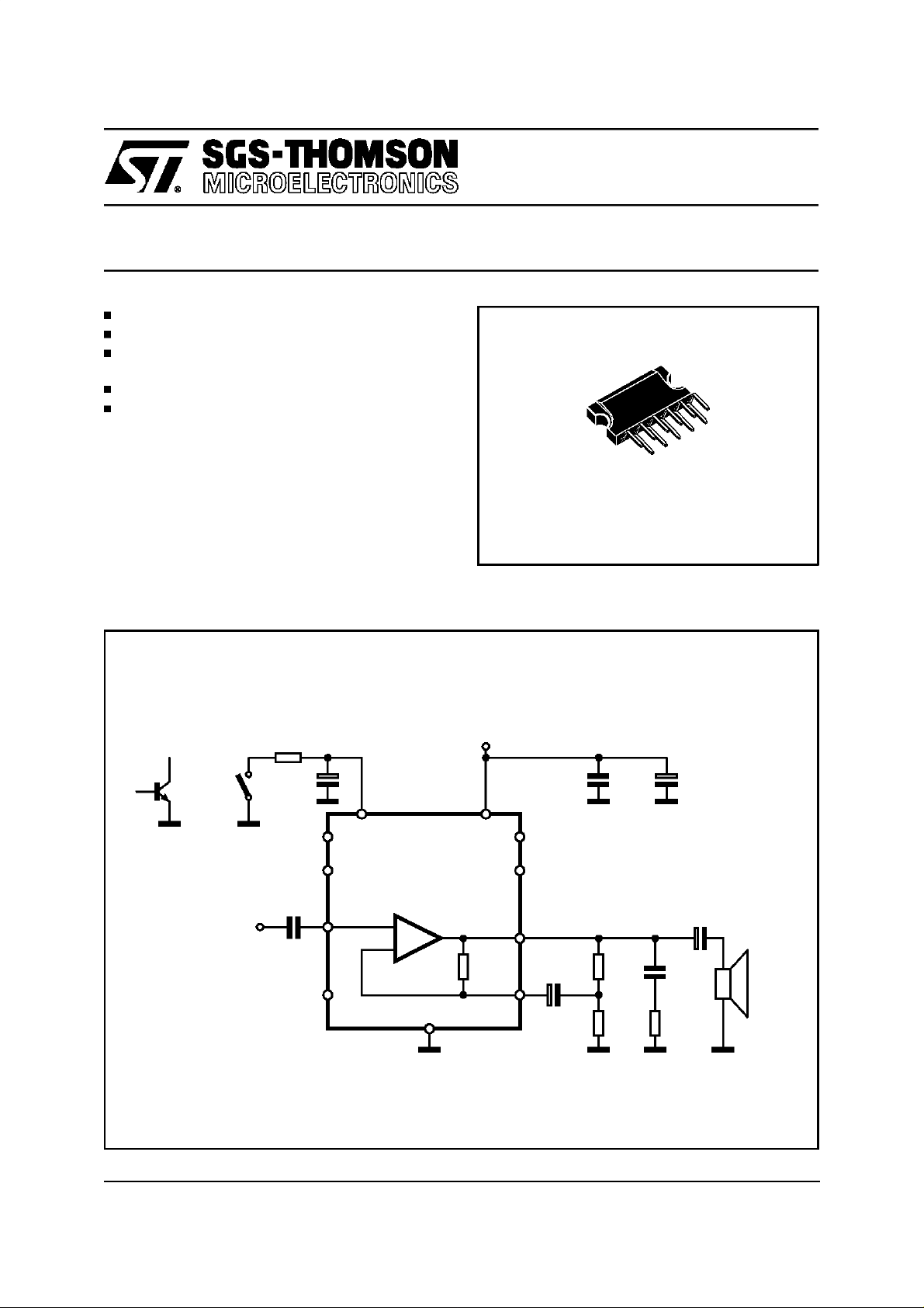
APPLICATIONCIRCUIT
R7 820
=
MUTE
SW
(L)
IN
CSVR
100µF
C2
100nF
3
1
11
TDA7253
7
27K
6
+V
9
S
10
2
8
4
D94AU130
Clipwatt11
C4
0.1µF
CF
47µF R4
R3
1.5K
47
C5
470µF
C11 1000µF
C9
0.1µF
R6
4.7
RL
May 1997
1/5

TDA7253
ABSOLUTE MAXIMUM RATINGS
Symbol Parameter Value Unit
Supply Voltage 35 V
Output Peak Current (repetitive f >20Hz) 2.5 A
Output Peak Current (nonrepetitive, t = 100µs) 3.5 A
Total PowerDissipation (T
=70°C) 25 W
case
Operating Temperature Range 0 to 70
Storage & Junction Temperature -40 to 150 °C
T
V
I
O
I
O
P
T
stg,Tj
S
tot
op
C
°
PIN CONNECTION
Figure 1:
ApplicationCircuit
(Topview)
11
10
9
8
7
6
5
4
3
2
1
N.C.
N.C.
+Vs
OUTPUT
N.C.
GND
NON INVERTING INPUT
INVERTING INPUT
SVR/MUTING
N.C.
N.C.
D93AU037A
2/5

THERMAL DATA
Symbol Parameter Value Unit
R
th j-case
Thermal resistancejunction to case Max 3 °C/W
TDA7253
ELECTRICALCHARACTERISTICS (Refer to the test and applicationcircuit, VS= 26V; RL=8
Gv= 30dB;f = 1KHz; T
=25°C unlessotherwise specified.)
amb
Ω;
Symbol Parameter Test Condition Min. Typ. Max. Unit
V
S
V
O
I
q
P
O
d Total Harmonic Distortion P
R
f
L
f
H
N Total Input Noise Voltage A Curve; RS = 10KΩ 2mV
e
SVR Supply Voltage Rejection R
VT
MUTE
VT
PLAY
A
M
I
qMUTE
Note: to avoid pop-on noise
Supply Voltage 10 32 V
Quiescent Output Voltage 12.5 V
Total Quiescent Current 40 mA
Output Power d = 10%
d=1%
= 1W 0.03 %
O
Input Resistance 100 200 K
I
810
8
Low Frequency Roll-off(-3dB) 40 Hz
High Frequency Roll-off (-3dB) 80 KHz
f = 22Hzto 22KHz; R
= 10KΩ; f= 100Hz; Vr= 0.5V 60 dB
S
= 10K
S
Ω
2.5 10
Mute Threshold 0.8 V
Play Threshold 5 V
Mute Attenuation 80 100 dB
Quiescent Current Mute 7 10 mA
C
F
≤ 1
C
SVR
W
W
Ω
V
µ
Figure 1:
Output Power vs. SupplyVoltage
Figure2:
Iq
(mA)
45
40
35
30
25
20
8 12 16 20 24 28 Vs(V)
QuiescentCurrent vs. Supply Voltage
D94AU131
3/5

TDA7253
CLIPWATT11PACKAGE MECHANICAL DATA
DIM.
MIN. TYP. MAX. MIN. TYP. MAX.
A 3.10 0.122
B 1.10 0.04
C 0.15 0.006
D 1.50 0.059
E 0.52 0.02
F 0.80 0.03
G 1.70 0.066
G1 17.00 0.66
H1 12.00 0.48
H3 20.00 0.79
L 17.90 0.70
L1 14.40 0.57
L2 11.00 0.43
M 2.54 0.1
M1 2.54 0.1
mm inch
4/5

TDA7253
Information furnished is believed to be accurate and reliable. However, SGS-THOMSON Microelectronics assumes no responsibilityfor the
consequences of use of such information norfor any infringement of patents or other rights ofthird parties which may result from its use.No
license is granted by implication or otherwise under any patent or patent rightsof SGS-THOMSON Microelectronics. Specification mentioned
in this publication are subject to change without notice. This publication supersedes and replaces all information previously supplied. SGSTHOMSON Microelectronics products are not authorized for use as critical components in life support devices or systems without express
written approval ofSGS-THOMSON Microelectronics.
1997SGS-THOMSON Microelectronics – Printed inItaly– All RightsReserved
SGS-THOMSON Microelectronics GROUP OF COMPANIES
Australia - Brazil - Canada- China - France - Germany - HongKong - Italy - Japan - Korea - Malaysia - Malta - Morocco - The Netherlands -
Singapore - Spain- Sweden - Switzerland- Taiwan - Thailand - UnitedKingdom - U.S.A.
5/5
 Loading...