

.WIDESUPPLYVOLTAGERANGE: 20TO90V
(± 10 to ± 45V)
.VERY LOW DISTORTION
.AUTOMATICQUIESCENTCURRENT
CONTROL FOR THE POWER TRANSISTORS
WITHOUTTEMPERATURESENSE
ELEMENTS
.OVERLOAD CURRENT PROTECTION FOR
THEPOWERTRANSISTORS
.MUTE/STAND-BYFUNCTIONS
.LOW POWER CONSUMPTION
.OUTPUTPOWER60 W/8Ω AND100 W/4Ω
DESCRIPTION
The TDA7250 stereo audio driver is designed to
drivetwo pair ofcomplementaryoutputtransistor in
the Hi-Fipower amplifiers.
TDA7250
60 W HI-FIDUAL AUDIO DRIVER
DIP20
ORDERING NUMBER : TDA7250
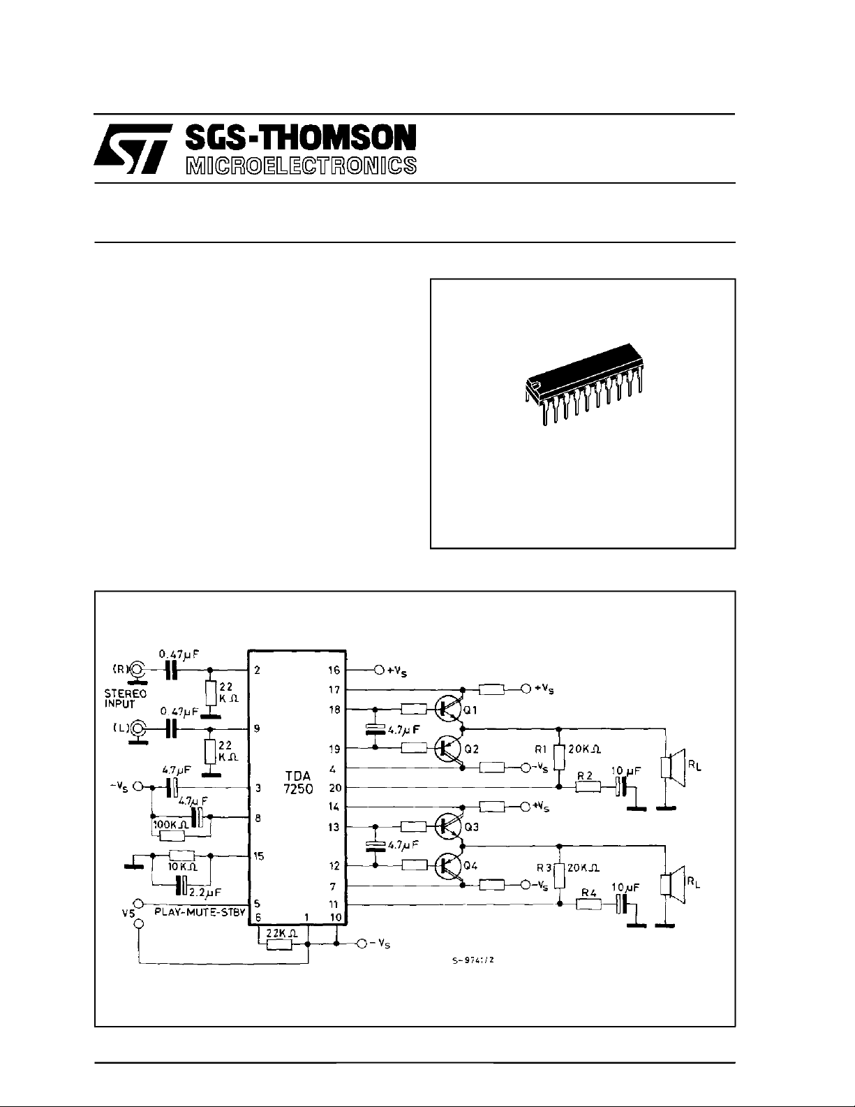
APPLI CATI O N CIR CUIT
March 1995
1/11
TDA7250
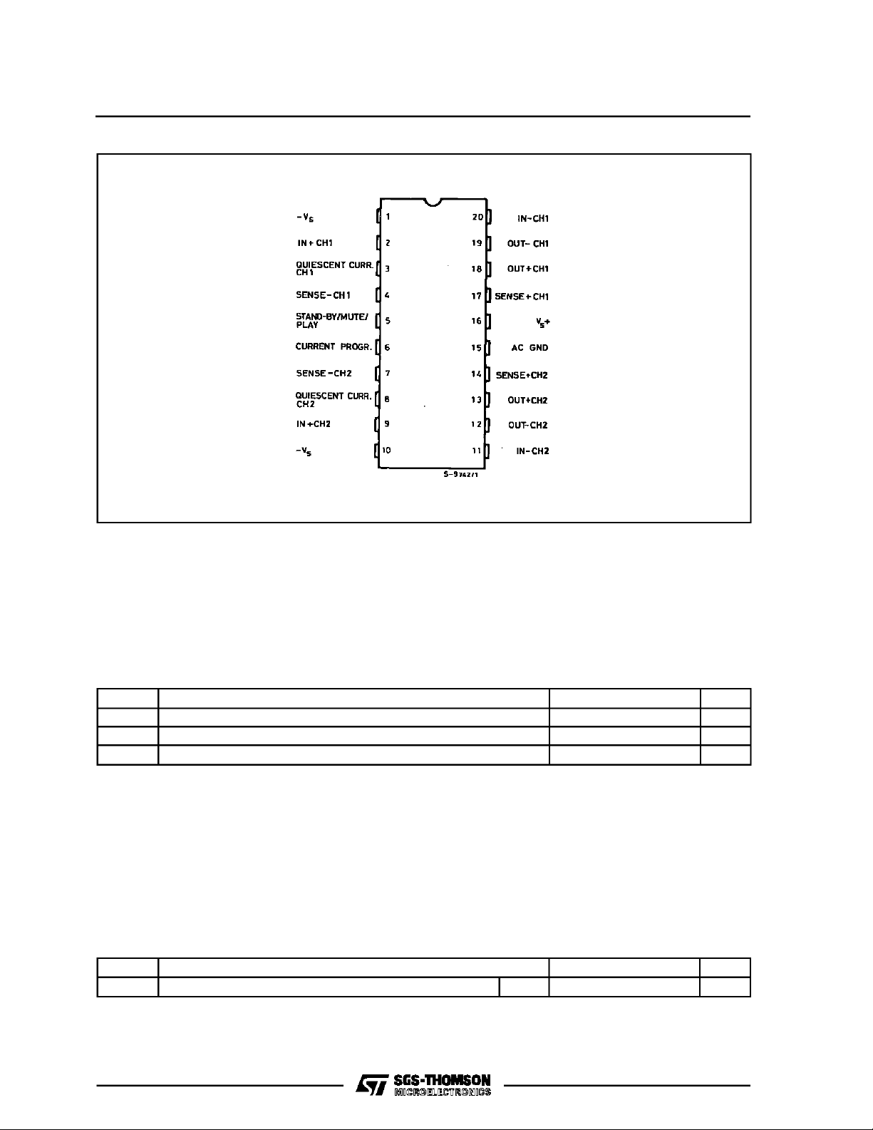
PIN CONNECTI O N (top view)
ABSOLUTE MAXIMUM RATINGS
Symbol Parameter Value Unit
Supply Voltage 100 V
V
s
P
T
j,Tstg
Power Dissipation at T
tot
Storage and Junction Temperature – 40 to + 150 °C
=60°C 1.4 W
amb
THERMAL DATA
Symbol Parameter Value Unit
R
2/11
th j-amb
Thermal Resistance Junction-ambient Max. 65 °C/W
TDA7250
PIN FUNCTIONS
N° Name Function
1V
2 NON–INV. INP. CH. 1 Channel 1 Input Signal.
3 QUIESC. CURRENT
4 SENSE (–) CH. 1 Negative voltage sense input for overload protection and for automatic quiescent
5 ST. BY / MUTE / PLAY Three-functions Terminal.
6 CURRENT PROGRAM High Impedance Power-stages Monitor.
7 SENSE (–) CH. 2 Negative Voltage Sense Input for Overload Protection and for Automatic
8 QUIESC. CURRENT
9 NON–INV. INP. CH. 2 Channel 2 Input Signals.
10 V
11 INVERT. INP. CH. 2 Feedback from Output (channel 2).
12 OUT (–) CH. 2 Out Signal to Lower Driver Transistor of Channel 2.
13 OUT (+) CH. 2 Out Signal to Higher Driver Transistor of Channel 2.
14 SENSE (+) CH. 2 Positive Voltage Sense Input for Overload Protection and for Automatic
15 COMMON AC GROUND AC Input Ground in MUTE Condition.
16 V
17 SENSE (+) CH. 1 Positive Voltage Sense Input for Overload Protection and for Automatic
18 OUT (+) CH. 1 Out Signal to High Driver Transistor of Channel 1.
19 OUT (–) CH. 1 Out Signal to Low Driver Transistor of Channel 1.
20 INVERT. INP. CH. 1 Feedback from Output (channel 1).
– POWER SUPPLY Negative Supply Voltage.
S
This capacitor works as an integrator, to control the quiescent current to output
CONTR. CAP. CH1
devices in no-signal conditions on channel 1.
current control.
For V
= 1 to 3 V, the device is in MUTE and only quiescent current flows in
IN
the power stages ; - for V
quiescent current is present in the power stages ; - for V
Quiescent Current Control.
This capacitor works as an integrator, to control the quiescent current to output
CONTR. CAP. CH. 2
devices in no-signal conditions on channel 2. If the voltage at its terminals drops
under 250 mV, it also resets the device from high-impedance state of output
stages.
– POWER SUPPLY Negative Supply Voltage.
s
Quiescent Current Control.
+ POWER SUPPLY Positive Supply Voltage.
S
Quiescent Current Control.
< 1 V, the device is in STAND-BY mode and no
IN
> 3 V, the devic
IN
3/11
TDA7250
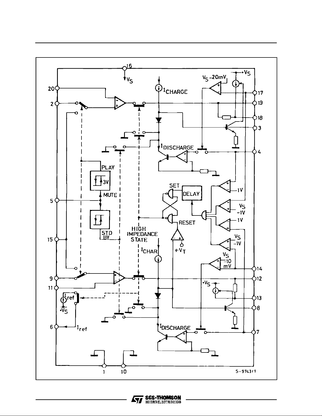
BLOCK DIAGRAM
4/11

TDA7250
ELECTRICAL CHARACTERISTICS (T
=25°C, Vs= ± 35 V, play mode, unless otherwise
amb
specified)
Symbol Parameter Test Conditions Min. Typ. Max. Unit
V
Supply Voltage ± 10 ± 45 V
s
Quiescent Drain Current Stand-by Mode 8 mA
I
d
Play Mode 10 14
Input Bias Current 0.2 1 µA
I
b
V
Input OffsetVoltage 1 ± 10 mV
os
Input OffsetCurrent 100 200 nA
I
os
Open Loop Voltage Gain f = 100 Hz 90 dB
G
v
f = 10 kHz 60
Input Noise Voltage RG= 600 Ω
e
N
B = 20 Hz to 20 kHz
SR Slew Rate 10 V/µs
d Total Harmonic Distortion G
= 26 dB, Po=40W
v
f = 1 kHz
f = 20 kHz
V
Output Voltage Swing 60 V
opp
P
Output Power (*) Vs= ± 35 V, RL=8Ω
o
I
Output Current ± 5mA
o
=±30 V, RL=8Ω
V
s
=±35 V, RL=4Ω
V
s
SVR Supply Voltage Rejection f = 100 Hz 75 dB
Channel Separation f = 1 kHz 75 dB
C
s
3 µV
0.004
0.03
60
40
100
%
%
pp
W
W
W
MUTE / STANDBY/ PLAY FUNCTIONS
Symbol Parameter Test Conditions Min. Typ. Max. Unit
Input Current (pin 5) 0.1 µA
I
i
Comparator Standby / Mute
V
th
1.0 1.25 1.5 V
Threshold (**)
H Hysteresis Standby / Mute 200 mV
Comparator Mute / Play
V
th
2.4 3.0 3.6 V
Threshold (**)
H Hysteresis Mute / Play 300 mV
Mute Attenuation f = 1 kHz 60 dB
Input Voltage Max. (pin 5) 12 (**) V
V
i
(*) Application circuit of fig. 1 f = 1 KHz ; d = 0.1 % ; Gv=26dB.
(**) Referred to − V
.
s
CURRENT SURVEY CIRCUITRY
Symbol Parameter Test Conditions Min. Typ. Max. Unit
Comparator Reference to + V
Delay Time 10 µs
t
d
to – V
S
S
0.8
0.8
1
1
1.4
1.4
QUIESCENTCURRENT CONTROL
Symbol Parameter Test Conditions Min. Typ. Max. Unit
Capacitor Current Charge
Discharge
Comparator Reference to + V
to – V
S
S
30
250
10 20
60
500
25 mV
10
V
V
µA
µA
mV
5/11

TDA7250
Figure 1 : ApplicationCircuit withPower Darlingtons.
Note : Q1/Q2 = Q3/Q4= TIP 142/TIP147
GV = 1 +R1/R2
6/11

TDA7250
Figure 2 : OutputPower vs. SupplyVoltage.
Figure 4 : ChannelSeparation.
Figure3 : Distortionvs.OutputPower(*).
Figure5 : Supply VoltageRejectionvs.
Frequency.
Figure 6 : QuiescentCurrentvs. SupplyVoltage. Figure7 : QuiescentCurrentvs. T
amb
.
7/11

TDA7250
Figure8 : Total DissipatedPower vs. Output
Powe r (*).
Figure 10 : Play-muteStandbyOperation.
Figure 9 : Efficiencyvs. OutputPower(*).
(*) Complet e circuit
8/11

Figure 11 : ApplicationCircuit Using Power Transistors.
TDA7250
Figure 12 : SuggestedTransistor Types for Various Loads and Powers.
RL=8Ω TL=4Ω
15W +30W +50W +70W
BDX
53/54A
BDX
53/54B
BDW
93/94B
TIP
142/147
30W +50W +90W +130W
BDW
93/94A
BDW
93/94B
BDV
64/65BMJ11013/11014
9/11

TDA7250
DIP20 PACKAGE MECHANICAL DATA
DIM.
MIN. TYP. MAX. MIN. TYP. MAX.
a1 0.51 0.020
B 0.85 1.40 0.033 0.055
b 0.50 0.020
b1 0.38 0.50 0.015 0.020
D 24.80 0.976
E 8.80 0.346
e 2.54 0.100
e3 22.86 0.900
F 7.10 0.280
I 5.10 0.201
L 3.30 0.130
Z 1.27 0.050
mm inch
10/11

TDA7250
Information furnished is believed to be accurate and reliable. However, SGS-THOMSON Microelectronics assumes no responsibility for
the consequences of use of such information nor for any infringement of patents or other rights of third parties which may result from its
use. No license is granted by implication or otherwise under any patent or patent rights of SGS-THOMSON Microelectronics. Specifications mentioned in this publication are subject to change without notice. This publication supersedes and replaces all information previously supplied. SGS-THOMSON Microelectronics products are not authorized for use as critical components in life support devices or
systems without express written approval of SGS-THOMSON Microelectronics.
1995 SGS-THOMSON Microelectronics - All Rights Reserved
Australia - Brazil - France - Germany - Hong Kong - Italy - Japan - Korea - Malaysia - Malta - Morocco - The Netherlands - Singapore-
SGS-THOMSON Microelectronics GROUP OF COMPANIES
Spain - Sweden - Switzerland - Taiwan - Thaliand - United Kingdom - U.S.A.
11/11
 Loading...