

5W AUDIO AMPLIFIER WITH MUTINGAND STAND-BY
MUTINGAND STAND-BYFUNCTIONS
VOLTAGERANGEUP TO 30V
HIGHSUPPLYVOLTAGE REJECTION
SVR TYP= 50dB (f = 100Hz)
MUSICPOWER= 12W (R
PROTECTIONAGAINSTCHIP OVER
TEMPERATURE
=4Ω, d = 10%)
L
TDA7245
Powerdip 9+9
DESCRIPTION
The TDA7245 is a monolithic integrated circuit in
9+9 POWERDIP package, intended for use as
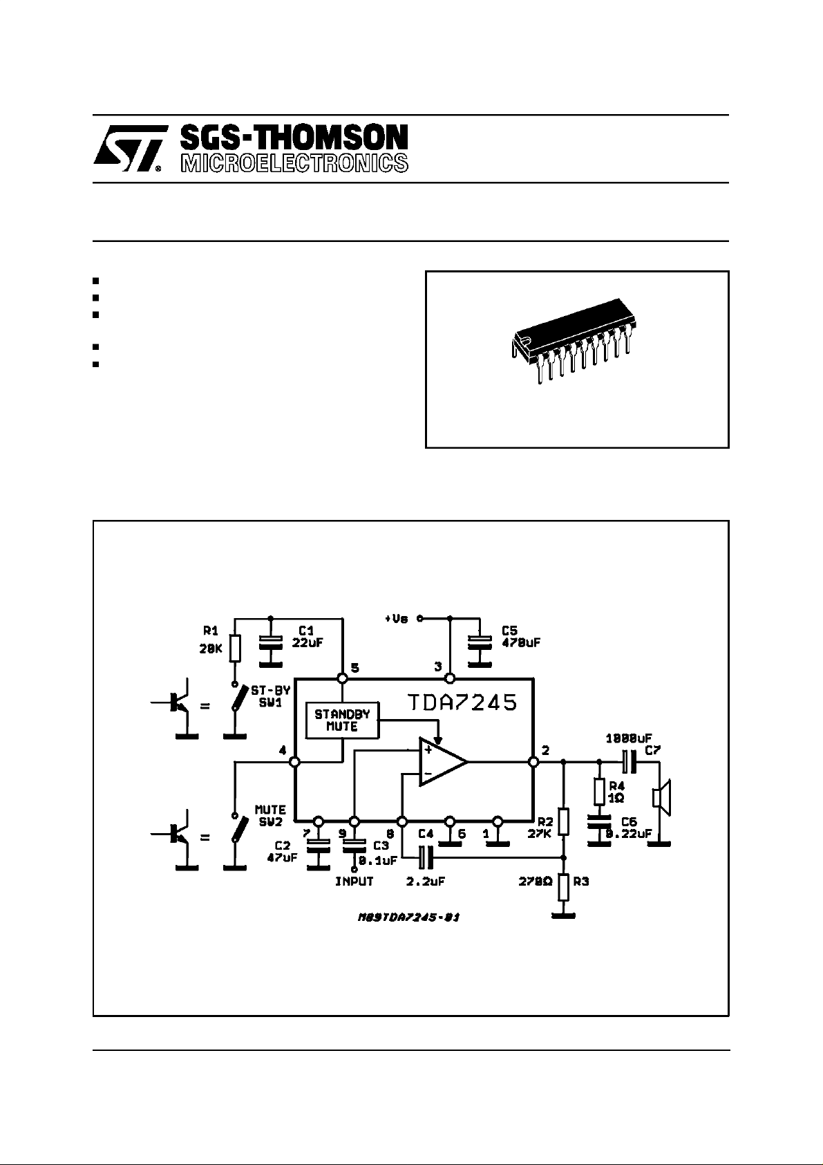
Figure1:
Testand ApplicationCircuit
ORDERING NUMBER: TDA7245
low frequency power amplifier in a wide range of
applicationsin radio and TV sets.
March 1995
1/11
TDA7245
ABSOLUTE MAXIMUM RATINGS
Symbol Parameter Value Unit
Supply Voltage 30 V
S
Output PeakCurrent (non repetitive t = 100µs) 3 A
Output PeakCurrent (repetitive, f > 20Hz) 2.5 A
Power Dissipation at T
at T
amb
case
=80°C
=70°C
1
6
Storage and junction Temperature -40 to 150
P
T
stg,Tj
V
I
O
I
O
tot
W
W
°
C
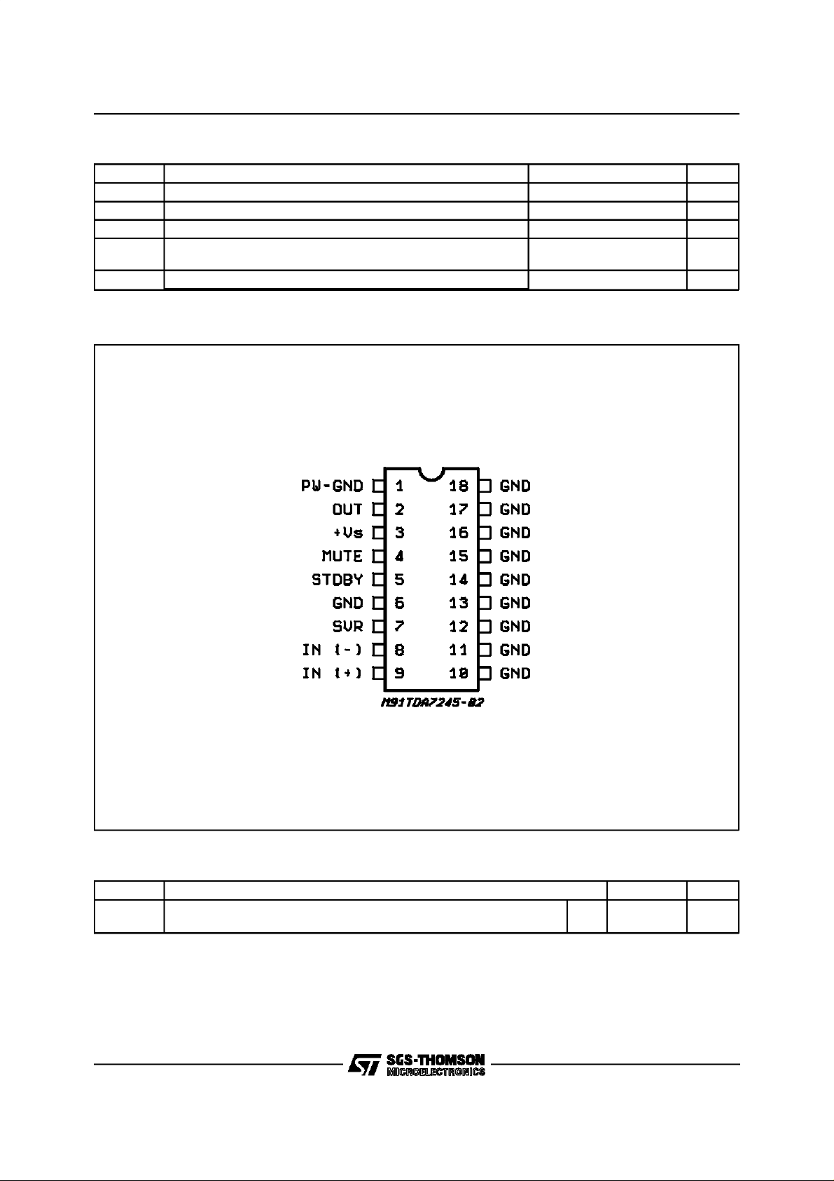
PIN CONNECTION
(Topview)
THERMAL DATA
Symbol Description Value Unit
2/11
R
th j-case
Rth j-amb
Thermal Resistance junction-case
Thermal Resistance junction-ambient
Max
Max
15
70
C/W
°
C/W
°
TDA7245
ELECTRICAL CHARACTERISTICS (Refer to the test circuit, T
=25°C,f = 1kHz; unless otherwise
amb
specified).
Symbol Parameter Test Condition Min. Typ. Max. Unit
V
S
V
O
I
d
P
O
d Harmonic Distortion V
R
I
BW Small signal bandwidth (-3dB) P
G
V
G
V
e
N
S/N Signal to Noise Ratio V
SVR Supply Voltage Rejection V
T
sd
Supply Voltage 12 30 V
Quiescent Output Voltage VS= 24V 11.6 V
Quiescent Drain Current VS= 14V
V
= 28V
S
17
21 35
Output Power d = 1%, f = 1KHz
V
= 14V, RL=4Ω
S
V
= 18V, RL=8Ω
S
4
4
d = 10%, f = 1KHz
= 14V, RL=4Ω
V
S
V
= 18V, RL=8
S
Ω
4
5
5
Music Power (*)
= 24V, d = 10%, RL=4
V
S
= 14V, RL=4Ω,
S
P
= 50mW to 3W
O
f = 1KHz
f = 10KHz
V
= 18V, RL=8Ω,
S
P
= 50mW to 3.5W
O
f = 1KHz
f = 10KHz
V
= 22V, RL=16Ω,
S
P
= 50mW to 3W
O
f = 1KHz
f = 10KHz
Ω
12
0.15
0.8
0.12
0.5
0.08
0.4
0.5 %
Input Impedance f = 1kHz 30 k
=1W;RL=4Ω VS= 14V 50 to 40,000 Hz
O
Voltage Gain (open loop) f= 1kHz 75 dB
Voltage Gain (closed loop) f = 1kHz 39 40 41 dB
Total Input Noise B = 22 - 22,000Hz
R
Thermal shut-down Junction
=50Ω
s
R
=1k
Ω
s
R
= 10k
Ω
s
= 18V; RL=8Ω
S
P
=5W; RS= 10K
O
= 16.5V; RL=8Ω; f = 100Hz
S
R
= 10kΩ;Vr= 0.5Vrms
s
Ω
40 50 dB
1.7
2
36
86 dB
150 °C
Temperature
mA
mA
W
W
W
W
W
%
%
%
%
%
Ω
mV
µ
µ
V
V
MUTE FUNCTION
Symbol Parameter Test Condition Min. Typ. Max. Unit
V
ATT
m
Pin 4 DC Voltage Mute SW Open (play) 6.4 V
Muting Attenuation f = 100Hz to 10kHz 60 65 dB
m
3/11
TDA7245
ELECTRICALCHARACTERISTCS
(Continued)
STAND-BYFUNCTION
Symbol Parameter Test Condition Min. Typ. Max. Unit
V
st-by
I
st-by
ATT
st-by
V
t
I
d st-by
Note (*):
MUSIC POWER CONCEPT
MUSIC POWER is ( according to the IEC clauses n.268-3 of Jan 83) the maximal power which the amplifier is capable of producing across the
rated load resistance (regardless of non linearity) 1 sec after the application of a sinusoidal input signal of frequency 1KHz.
According to this definition our method of measurement comprises the followingsteps:
1) Set the voltage supply at the maximum operating value -20%
2) Apply a input signal in the form of a 1KHz tone burst of 1 sec duration; the repetition period of the signal pulses is > 60 sec
3) The output voltage is measured 1 sec from thestart of the pulse
4) Increase the input voltage until the output signal show a THD = 10%
5) The music power is thenV
The target of this method isto avoid excessive dissipation in theamplifier.
Pin 5 DC Voltage Mute SW Open (play) 6.4 V
Pin 5 Current Mute SW Closed (st-by) 160 280
µ
Stand-by Attenuation f = 100Hz to 10kHz 70 90 dB
Stand-by Threshold (pin 5) 3.8 V
Stand-by Current VS= 14V 1 3 mA
2
/R1,where V
out
isthe output voltage measured in the condition of point 4) and R1 is the ratedload impedance
out
A
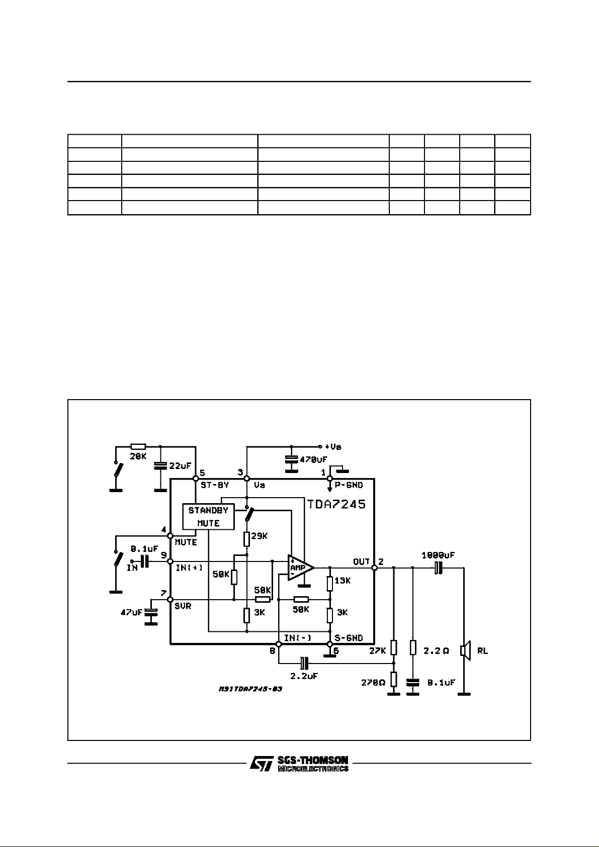
Figure 2: Schematic Diagram
4/11

Figure 3: P.C. Board and ComponentsLayout of the Circuit of fig2 (1:1 scale)
TDA7245
APPLICATIONSUGGESTIONS
The recommended values of the external componentsare those shown on the application circuit of fig.1.
Different values can be used. The following table can help the dsigner.
Component Rec. Value Purpose Larger than Rec. Value Smaller than Rec. Value
R1 20K
R2(*) 27KΩ Feedback
R3(*) 270
R4 1
C1 22µF St-By Capacitor Longer ON/OFF Delay
C2 47µF SVR Capacitor Worse Turn-On POP by
C3 0.1µF Input Capacitance Higher Low Frequency
C4 2.2µF InvertingInput DC
C5 470µF Supply Voltage Danger of Oscillations
C6 0.22µF Frequency Stability Danger of Oscillations
C7 1000µF Output DC Decoupling Higher Low Frequency
(*) The value of closed loop gain (GV= 1 + R2/R3) must be higher than 25dB.
Ω
Ω
Ω
St-By Biasing Incorrect St-By Function Worse POP and Shorter
Resistors
Frequency Stability Danger of Oscillations
Decoupling
Increase of Gain Decrease of Gain
Decrease of Gain Increase of Gain
Time at St-By IN/OUT
V
and St-By
S
Delay at St-By Insertion
Worse POP and Shorter
Delay at St-By insertion
Degradation of SVR
Cut-off
Higher Low Frequency
Cut-off
Cut-off
5/11

TDA7245
Figure 4:
DC Output Voltage vs. Supply Voltage
Figure 6: Output Power vs. Supply Voltage
Figure5:
vs.Supply Voltage
I
D
Figure7: Output Power vs. Supply Voltage
Figure 8: Output Power vs. Supply Voltage
6/11
Figure9: Distortionvs. Output Power

TDA7245
Figure 10: Distortionvs. OutputPower
Figure 12: SupplyVoltage Rejection vs.
Frequency(play)
Figure11: Distortionvs. Output Power
Figure13: PowerDissipation & Efficiency vs.
OutputPower
Figure 14:
PowerDissipation& Efficiency vs.
OutputPower
Figure15:
(=V
V
pin5
) vs. Supply Voltage
pin4
7/11

TDA7245
Figure 16: I
(muting)vs. Supply Voltage
pin4
Figure 18: QuiescentCurrent (St-By) vs. Supply
Voltage
Figure17: I
Figure19:
(St-By)vs. SupplyVoltage
pin5
OutputAttenuationvs. V
pin5
Figure 20:
8/11
QuiescentCurrent vs. V
pin5
MUTING/ STAND- BY
The muting function allows to inhibit the output
signal through an external control signal.
It can be used in many cases, when a temporary
inhibition of the output signal is requested, for example:
– in switch-oncondition, to avoid preamplifier
power-ontransients
– during switching at the input stages
– during the receivertuning.
The stand-by function is veryuseful and permits a
complete turn ON/OFF of the device through a
low power signal, which can be providedby a µP.

TDA7245
THERMAL SHUTDOWN
The presence of a thermal limiting circuit offers
the following advantages:
1)An overload on the output (even if it is permanent), or an above limit ambient temperature
can be easily tolerated since the Tj cannot be
higherthan 150°C.
2)The heatsink can have a smaller factor of
safety compared with that of a conventional
circuit. There is no possibility of device damage due to high junctiontemperature.
If for any reason, the junction temperatureincrease up to 150°C, the thermal shutdown
simply reduces the power dissipation and the
currentconsumption.
The maximum allowable power dissipation depends upon the junction-ambient thermal resistance. Fig. 21 shows this dissipable power as a
function of ambient temperature for different thermal resistance.
Figure 21:
MaximumAllowable Power
Dissipation vs. Ambient Temperature
MOUNTINGINSTRUCTIONS
The TDA7245 is assembledin the POWERDIP, in
which 9 pins (from 10 to 18) are attached to the
frame and removethe heat produced by the chip.
Figure 22 shows a PC Board copper area used
as a Heatsink (l = 65mm). The Thermal ResistanceJunction-Ambientis 35°C.
Figure22:
Exampleof Heatsink using PC Board
Copper (l = 65mm)
9/11

TDA7245
POWERDIP18 (9+9) PACKAGE MECHANICAL DATA
DIM.
MIN. TYP. MAX. MIN. TYP. MAX.
a1 0.51 0.020
B 0.85 1.40 0.033 0.055
b 0.50 0.020
b1 0.38 0.50 0.015 0.020
D 24.80 0.976
E 8.80 0.346
e 2.54 0.100
e3 20.32 0.800
F 7.10 0.280
I 5.10 0.201
L 3.30 0.130
Z 2.54 0.100
mm inch
10/11

TDA7245
Information furnished is believed to be accurate and reliable. However, SGS-THOMSON Microelectronics assumes no responsibility for the
consequences of use of such information nor for any infringement of patents or other rights of third parties which may result from its use. No
license is granted by implication or otherwise under any patent or patent rights of SGS-THOMSON Microelectronics. Specification mentioned
in this publication are subject to change withoutnotice. This publication supersedes and replaces all information previously supplied. SGSTHOMSON Microelectronics products are not authorized for use as critical components in life support devices or systems without express
written approval of SGS-THOMSON Microelectronics.
1996 SGS-THOMSON Microelectronics – Printed inItaly – All RightsReserved
SGS-THOMSON Microelectronics GROUPOF COMPANIES
Australia - Brazil - Canada- China - France - Germany - Hong Kong - Italy - Japan - Korea - Malaysia - Malta- Morocco - The Netherlands-
Singapore - Spain - Sweden - Switzerland- Taiwan - Thailand - UnitedKingdom - U.S.A.
11/11
 Loading...