


20W BRIDGE AMPLIFIER FOR CAR RADIO
VERYLOW STAND-BY CURRENT
GAIN= 32dB
OUTPUT PROTECTED AGAINST SHORT
CIRCUITS TO GROUND AND ACROSS
LOAD
COMPACTHEPTAWATTPACKAGE
DUMP TRANSIENT
THERMALSHUTDOWN
LOUDSPEAKERPROTECTION
HIGHCURRENT CAPABILITY
LOW DISTORTION/ LOWNOISE
DESCRIPTION
The TDA7241B is a 20W bridge audio amplifier
IC designed specially for car radio applications.
Thanks to the low external part count and compact Heptawatt 7-pin power package the
TDA7241B occupies little space on the printed
circuit board.
Reliable operation is guaranteed by a compre-
TDA7241B
Heptawatt
ORDERING NUMBER: TDA7241BH
hensive array of on-chipprotectionfeatures.
These include protection against AC and DC out-
put short circuits (to ground and across the load),
load dump transients, and junction overtemperature. Additionally, the TDA7241B protects the
loudspeaker when one output is short-circuitedto
ground.
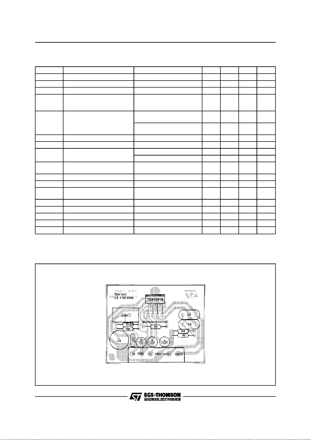
Figure 1: Test and Appliication Circuit
July 1997
1/7
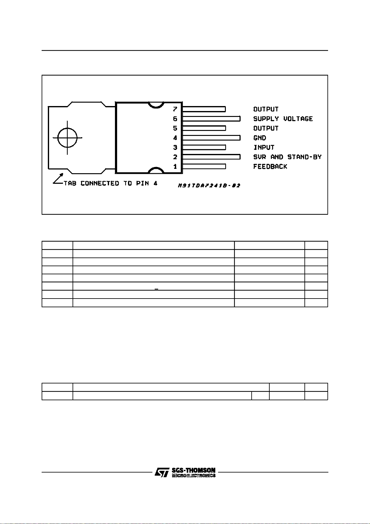
TDA7241B
PIN CONNECTION (Topview)
ABSOLUTE MAXIMUM RATINGS
Symbol Parameter Value Unit
V
V
V
I
O
I
O
P
tot
T
stg,Tj
Operating Supply Voltage 18 V
S
DC Supply Voltage 28 V
S
Peak Supply Voltage (t = 50ms) 40 V
S
Peak OutputCurrent (non repetitive t = 0.1ms) 4.5 A
Peak OutputCurrent (repetitive f > 10Hz) 3.5 A
Power Dissipationat T
=85°C16W
case
Storage and Junction Temperature -40 to 150 °C
THERMAL DATA
Symbol Description Value Unit
R
th j-case
Thermal Resistance Junction-case Max 4
C/W
°
2/7
TDA7241B
ELECTRICAL CHARACTERISTICS (Refer to the circuit of Fig. 1; VS= 14.4V; Rth(heatsink) = 4°C/W,
=25°C,unlessotherwise specified
T
amb
Symbol Parameter Test Condition Min. Typ. Max. Unit
V
S
I
d
V
OS
P
O
d Distortion R
G
V
SVR Supply Voltage Rejection f =100Hz R
E
n
η
I
sb
R
V
f
L
f
H
A
S
(pin.2) Stand-by Threshold 1 V
V
TH
T
sd
(*) B = Curve (**) B = 22Hz to 22KHz
Supply Range 18 V
Total Quiescent Current RL=4
Ω
Output OffsetVoltage 100 mV
Output Power . RL=2Ω
f = 1KHz d = 10% R
. R
=4
Ω
L
P
= 50mW to 12W
O
=8Ω f = 1KHz
R
L
P
= 50mW to 6W
O
=4Ω
L
=8
L
f = 1KHz
Ω
18
26
20
12
0.1 0.5 %
0.05 %
Voltage Gain f = 1KHz 31 32 33 dB
= 10KΩ 40 50 dB
g
Total InputNoise B = Curve A Rg= 10KΩ 2 µV
= 10KΩ 310mV
S
65 %
Efficiency R
B = 22Hz to 22KHz R
P
=4
L
= 20W
O
Ω
f = 1KHz
Stand-by Current 100 µA
Input Resistance f = 1KHz 70 KΩ
i
Input Sensitivity f = 1KHz
i
Low Frequency Roll Off (-3dB) PO= 15W RL=4
P
=2W RL=4
O
Ω
Ω
70 mV
30 Hz
High FrequencyRoll Off (-3dB) PO = 15W RL=4Ω 25 KHz
Stand-by Attenuation VO= 2Vrms 70 90 dB
ThermalShutdownJunctionTemp. 150
80 mA
W
C
°
Figure 2: P.C. Boardand ComponentLayout of the Circuit of Fig. 1 (1:1scale).
3/7
TDA7241B
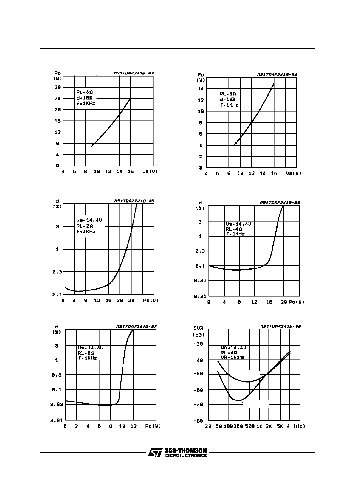
Figure 3: Output Power vs. SupplyVoltage
Figure 5: Distortion vs. OutputPower
Figure4: Output Power vs. SupplyVoltage
Figure6: Distortionvs. OutputPower
Figure 7: Distortion vs. OutputPower Figure8: SVR vs.Frequency
Rg= 10kΩ
R
=0
g
4/7
Ω

TDA7241B
Figure 9: Power Dissipation and Efficiencyvs.
OutputPower
Figure10: PowerDissipation andEfficiency vs.
OutputPower
5/7

TDA7241B
HEPTAWATT PACKAGEMECHANICAL DATA
DIM.
A 4.8 0.189
C 1.37 0.054
D 2.4 2.8 0.094 0.110
D1 1.2 1.35 0.047 0.053
E 0.35 0.55 0.014 0.022
F 0.6 0.8 0.024 0.031
F1 0.9 0.035
G 2.41 2.54 2.67 0.095 0.100 0.105
G1 4.91 5.08 5.21 0.193 0.200 0.205
G2 7.49 7.62 7.8 0.295 0.300 0.307
H2 10.4 0.409
H3 10.05 10.4 0.396 0.409
L 16.97 0.668
L1 14.92 0.587
L2 21.54 0.848
L3 22.62 0.891
L5 2.6 3 0.102 0.118
L6 15.1 15.8 0.594 0.622
L7 6 6.6 0.236 0.260
M 2.8 0.110
M1 5.08 0.200
Dia 3.65 3.85 0.144 0.152
MIN. TYP. MAX. MIN. TYP. MAX.
mm inch
6/7

TDA7241B
Information furnished is believed to be accurate and reliable. However, SGS-THOMSON Microelectronics assumes no responsibility for the
consequences of use of such information nor for any infringement of patents or other rights of third partieswhich may resultfrom its use. No
license is granted by implication or otherwise under any patent or patent rights of SGS-THOMSON Microelectronics. Specifications mentioned in this publication are subject to change withoutnotice. This publication supersedes and replaces all informationpreviously supplied.
SGS-THOMSON Microelectronics products are not authorized for use as critical components in life support devices or systems withoutexpress writtenapproval of SGS-THOMSON Microelectronics.
1997 SGS-THOMSON Microelectronics -All RightsReserved
HEPTAWATT is a Trademarkof SGS-THOMSONMicroelectronics
SGS-THOMSON Microelectronics GROUP OF COMPANIES
Australia - Brazil- Canada- China - France - Germany - HongKong - Italy - Japan- Korea - Malaysia - Malta- Morocco - The Netherlands-
Singapore - Spain- Sweden - Switzerland- Taiwan - Thailand - United Kingdom - U.S.A.
7/7
 Loading...