

20WBRIDGE AMPLIFIERFOR CAR RADIO
COMPACTHEPTAWATTPACKAGE
.
FEWEXTERNAL COMPONENTS
.
OUTPUT PROTECTEDAGAINSTSHORT
.
CIRCUITSTO GROUNDAND ACROSSLOAD
DUMP TRANSIENT
.
THERMALSHUTDOWN
.
LOUDSPEAKERPROTECTION
.
HIGHCURRENT CAPABILITY
.
LOWDISTORTION/LOWNOISE
.
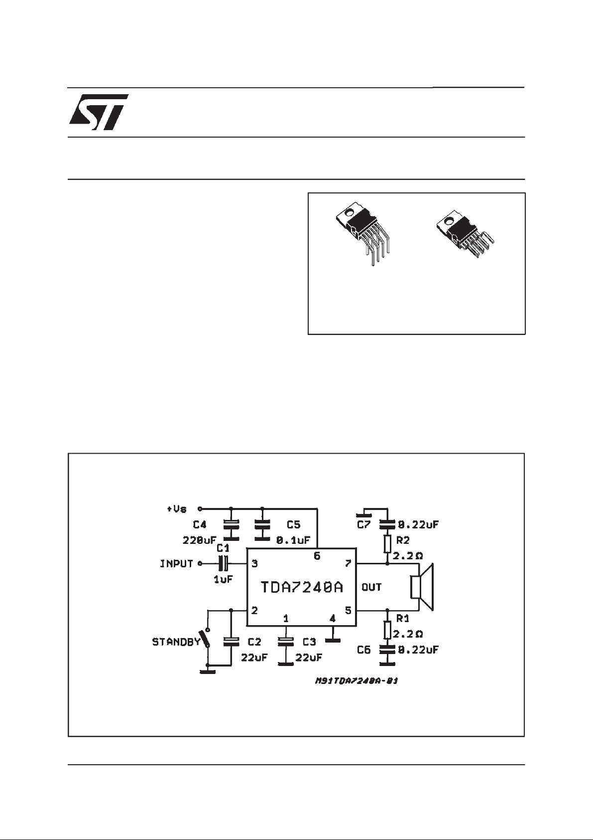
TDA7240A
Heptawatt H HeptawattV
ORDERING NUMBERS:
TDA7240AH TDA7240AV
DESCRI PTION
TheTDA7240A is a 20W bridge audio amplifierIC
designed specially for car radio applications.
Thanksto the low externalpart countand compact
Heptawatt 7-pin power package the TDA7240A
occupieslittlespaceon the printedcircuitboard.
Figure 1: Te st a nd A p p lica tion Circuit
Reliableoperationis guaranteedby a comprehensive arrayof on-chipprotectionfeatures.These include protection against AC and DC output short
circuits (togroundand across theload), loaddump
transients,and junction overtemperature. Additionally,theTDA7240Aprotectstheloudspeakerwhen
oneoutputisshort-circuitedto ground.
December1998
1/8
TDA7240A
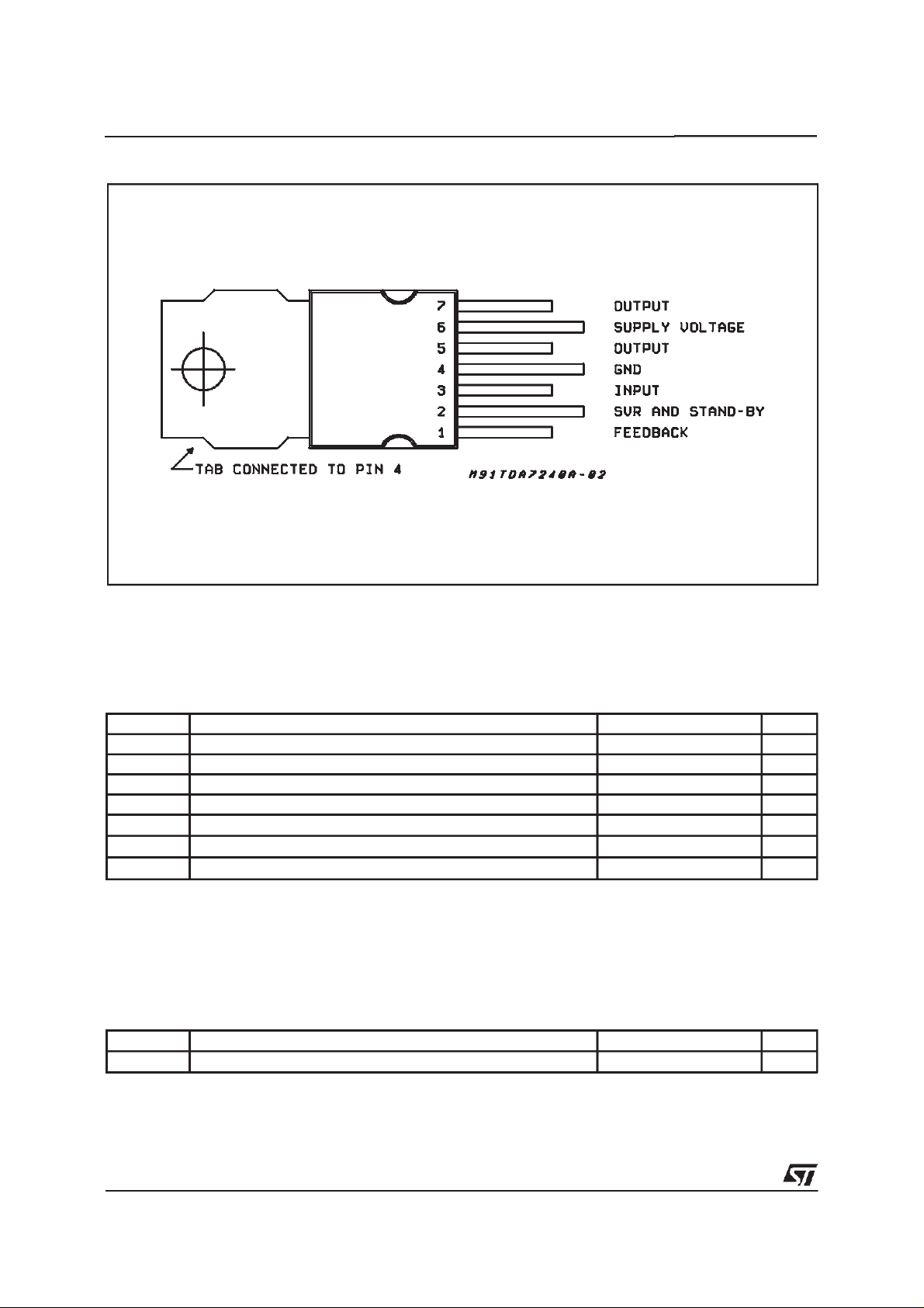
PIN CONNECTI O N (Top view)
ABSOLUTEMAXIMUMRATINGS
Symbol Parameter Value Unit
V
V
V
I
o
I
o
P
T
stg,Tj
(*)Internally limited
Operating Supply Voltage 18 V
s
DC Supply Voltage 28 V
s
Peak Supply Voltage(for 50ms) 40 V
s
(*) Peak Output Current (nonrepetitive t = 0.1ms) 4.5 A
(*)
Peak Output Current (repetitive f ≥10Hz)
Power Dissipation at Tcase = 85°C
tot
3.5 A
16 W
Storageand Junction Temperature –40 to 150
THERMALDATA
Symbol Parameter Value Unit
R
thj-case
ThermalResistance Junction-case Max. 4 V
°C
2/8
TDA7240A
ELECTRICAL CHARACTERISTICS (referto the circuitof fig.1,T
= 14.4V)
V
s
=25°C,Rth(heatsink)= 4°C/W,
amb
Symbol Parameter Test Conditions Min. Typ. Max. Unit
SupplyVoltage 18 V
V
s
OutputOffset Voltage 150 mV
V
os
TotalQuiescent Current
I
d
OutputPower f= 1kHz; d = 10%
P
o
d Distortion
R
L
R
L
P
o
R
L
P
o
=4Ω
=4
Ω
= 50mWto 12W
=8
Ω
= 50mWto 12W
=4Ω
R
L
=8
R
L
f = 1kHz
f = 1kHz
Ω
18
10
65 120 mA
20
12
0.1 0.5 %
0.05 0.5 %
GV VoltageGain f = 1KHz 39.5 40 40.5 dB
SVR SupplyVoltage Rejection
TotalInput Noise
E
N
Efficiency
η
Stand-byCurrent 200
I
sb
InputResistance f = 1kHz 70
R
i
InputSensitivity
V
i
Low Frequency Roll Off
f
L
(–3dB)
f
High Frequency Roll Off
H
f = 100Hz R
= 10KΩ
R
g
=4Ω f = 1KHz
R
L
f = 1kHz;P
Po = 15W; R
Po = 15W; RL = 4
= 2W; RL=4Ω
o
=4Ω
L
Ω
=10KΩ
g
(*)
(**)
35 40 dB
2
310
65 %
28 mV
30 Hz
25 kHz
(–3dB)
A
Stand-byAttenuation Vo= 2Vrms 70 90 dB
s
V
TH (pin2)
(*)B= Curve A (**)B = 22Hz to 22KHz
Stand-byThreshold 1 V
W
W
µV
µV
µA
kΩ
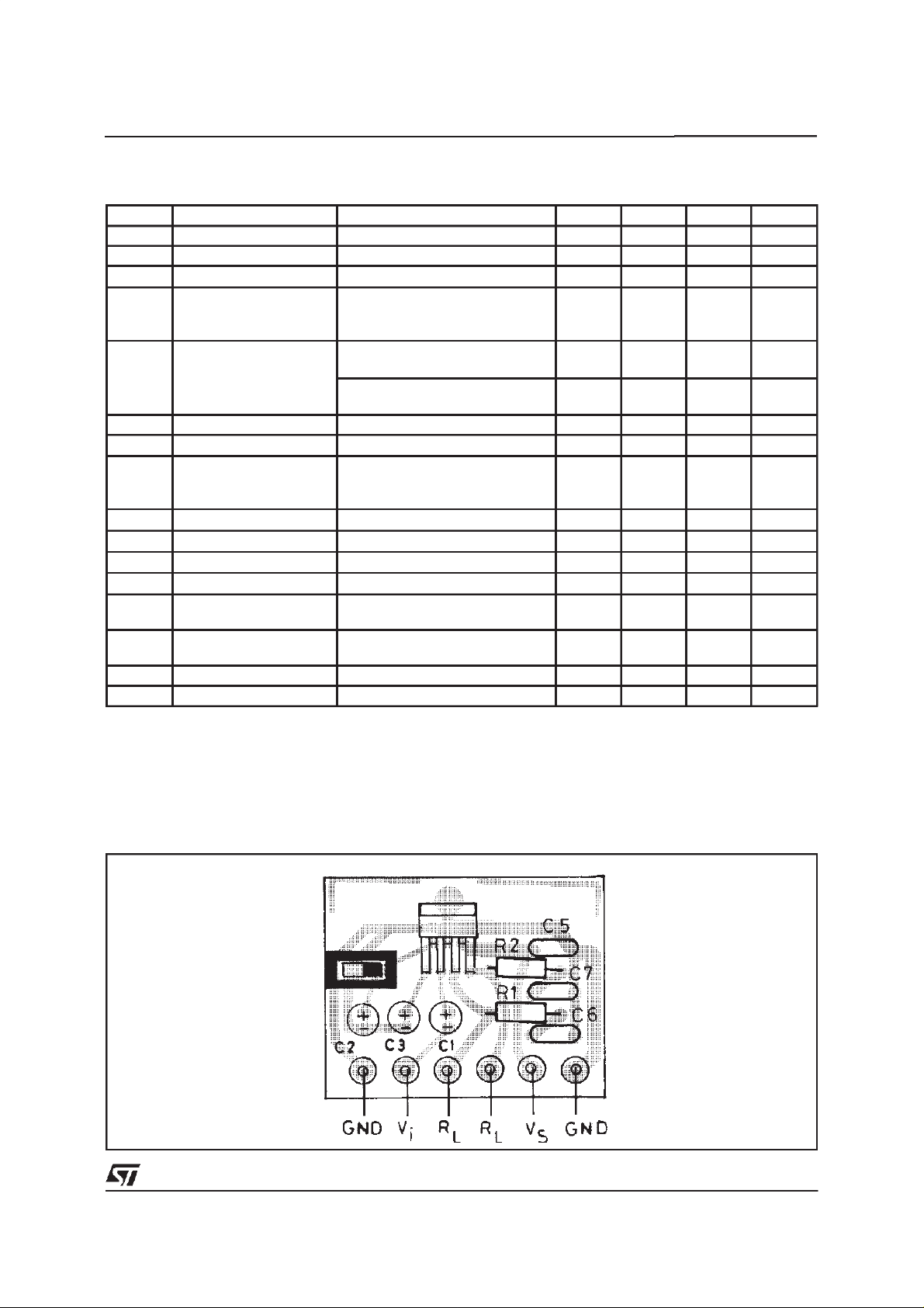
Figure2:P.C. Board and Components layout of the Circuit of Fig. 1.(1:1scale)
3/8

TDA7240A
APPLICATION SUGGESTION
TherecommendedvaluesofthecomponentsarethoseshownonapplicationcircuitofFig.1.Differentvalues
canbe used,the followingtablecan helpthe designer.
Component Recommended
Value
R1,R2
C1
C2
C3
C6,C7
C4
C5
2.2Ω FrequencyStability Danger of High
1µF
22µF
22µF
0.22µF
220µF
0.1µF
Purpose Larger Than SmallerThan
FrequencyOscillation
InputDC Decoupling Higher Turn On and
Stand-byDelay
Ripple Rejection Increaseof SVR
Increaseof the Turn
On Delay
Feedback low
FrequencyCutoff
FrequencyStability Danger of Oscillation
Supply Filter Danger of Oscillation
Supply Bypass Danger of Oscillation
Higher Turn On Pop.
Higher Low
FrequencyCutoff
Degradation of SVR
Higher Low Frequency
Cutoff
Figure 3 : OutputPowervs.SupplyVoltage.
Figure 4 : Distortionvs. OutputPower.
Figure 6 : Distortionvs. OutputPower.Figure5 : OutputPowervs. Supplyvoltage.
4/8

TDA7240A
Figure7 : Distortionvs. Frequency.
Figure 9 : PowerDissipationand Efficiencyvs.
OutputPower.
Figure 8 : SupplyVoltageRejection
vs. Frequency.
Figure10 : PowerDissipationandEfficiencyvs.
OutputPower.
5/8

TDA7240A
DIM.
MIN. TYP. MAX. MIN. TYP. MAX.
A 4.8 0.189
C 1.37 0.054
D 2.4 2.8 0.094 0.110
D1 1.2 1.35 0.047 0.053
E 0.35 0.55 0.014 0.022
E1 0.7 0.97 0.028 0.038
F 0.6 0.8 0.024 0.031
F1 0.9 0.035
G 2.34 2.54 2.74 0.095 0.100 0.105
G1 4.88 5.08 5.28 0.193 0.200 0.205
G2 7.42 7.62 7.82 0.295 0.300 0.307
H2 10.4 0.409
H3 10.05 10.4 0.396 0.409
L 16.7 16.9 17.1 0.657 0.668 0.673
L1 14.92
L2 21.24 21.54 21.84 0.386 0.848 0.860
L3 22.27 22.52 22.77 0.877 0.891 0.896
L4 1.29
L5 2.6 2.8 3 0.102 0.110 0.118
L6 15.1 15.5 15.8 0.594 0.610 0.622
L7 6 6.35 6.6 0.236 0.250
L9 0.2 0.008
M 2.55 2.8 3.05 0.100 0.110 0.120
M1 4.83 5.08 5.33 0.190 0.200 0.210
V4 40° (typ.)
Dia 3.65 3.85 0.144 0.152
mm inch
0.587
0.051
0.260
OUTLINE AND
MECHANICAL DATA
Heptawatt V
H3
L
VV
E
L1
M1
A
C
D
M
D1
H2
V4
L9
H1
L5
Dia.
L2
L3
F
E1
E
GG1G2
F
L7
L4
L6
F1H2
HEPTAMEC
6/8

TDA7240A
DIM.
MIN. TYP. MAX. MIN. TYP. MAX.
A 4.8 0.189
C 1.37 0.054
D 2.4 2.8 0.094 0.110
D1 1.2 1.35 0.047 0.053
E 0.35 0.55 0.014 0.022
F 0.6 0.8 0.024 0.031
F1 0.9 0.035
G 2.41 2.54 2.67 0.095 0.100 0.105
G1 4.91 5.08 5.21 0.193 0.200 0.205
G2 7.49 7.62 7.8 0.295 0.300 0.307
H2 10.4 0.409
H3 10.05 10.4 0.396 0.409
L 14.2 0.559
L1 4.4
L2 15.8
L3 5.1
L5 2.6 3 0.102 0.118
L6 15.1 15.8 0.594 0.622
L7 6 6.6 0.236
L9 4.44 0.175
Dia 3.65 3.85 0.144 0.152
mm inch
0.173
0.622
0.201
0.260
OUTLINE AND
MECHANICAL DATA
Heptawatt H
7/8

TDA7240A
Information furnished is believed to be accurate and reliable. However, STMicroelectronics assumes no responsibility for the consequences of use of such information nor for any infringement of patents or other rights of third parties which may result from its use. No
license is granted by implication or otherwise under any patent or patent rights of STMicroelectronics. Specification mentioned in this
publication are subject to change without notice. This publication supersedes and replaces all information previously supplied. STMicroelectronics products are not authorized for use as critical components in life support devices or systems without express written
approval of STMicroelectronics.
Australia - Brazil - Canada - China - France - Germany - Italy - Japan - Korea - Malaysia - Malta - Mexico - Morocco - The Netherlands -
Singapore - Spain - Sweden - Switzerland - Taiwan - Thailand - United Kingdom - U.S.A.
The ST logo is a registered trademark of STMicroelectronics
HEPTAWATT is a Trademark of SGS-THOMSON Microelectronics
1998 STMicroelectronics – Printed in Italy – All Rights Reserved
STMicroelectronics GROUP OF COMPANIES
http://www.st.com
8/8
 Loading...